Design and implementation of near-memory computing array architecture based on shared buffer①
2022-02-11SHANRuiGAOXuFENGYaniHUIChaoCUIXinyueCHAIMiaomiao
SHAN Rui(山 蕊),GAO Xu,FENG Yani,HUI Chao,CUI Xinyue,CHAI Miaomiao
(*School of Electronic Engineering,Xi’an University of Posts and Telecommunications,Xi’an 710121,P.R.China)
(**School of Computer,Xi’an University of Posts and Telecommunications,Xi’an 710121,P.R.China)
Abstract
Key words:near-memory computing,shared buffer,reconfigurable array processor,convolutional neural network(CNN)
0 Introduction
At present,central processing unit(CPU)+graphics processing unit(GPU)is often used to accelerate convolutional neural network(CNN),but it is inevitable to transfer a large amount of data between CPU memory and GPU memory.The long delay generated by data transmission limits the improvement of system performance[1].As the scale of deep learning is getting larger and larger,it puts high demands on computing performance and memory space.The problem of‘Memory Wall’caused by the mismatch of processing speed and memory speed has become increasingly serious[2].In order to reduce access latency and increase computing speed,hierarchical memory structures such as multi-level cache technology are generally used to reduce access latency[3].However,the three-level memory structure composed of registers,cache,and dynamic random access memory(DRAM)is difficult to meet the high bandwidth and high energy efficiency requirements of new applications for memory access.For the moment,large-scale processing systems are shifting from a traditional computing-centric model to a datacentric model[4].A general near-data processing architecture was proposed in Ref.[5],which is suitable for concurrent data structures such as linked list,skip list,and the first-in-first-out queue.However,the experiment analysis shows that the potential benefits of concurrent data structures based on near-data processing are not ideal.Efficient synchronization between the near-data processing cores is essential to give full play to near-data processing and achieve the high performance of parallel workloads.Due to the lack of shared cache and hardware cache consistency,supporting inter-core synchronous communication is still a challenge for many near-data processing structures[6].Due to the limitations of DRAM technology,the processing efficiency of the past near-data processing(NDP)is not good.However,with the advancement of through silicon via(TSV)technology,three-dimensional(3D)stacked memory has been developed,which enables logic chips and DRAM chips to coexist,making NDP easier to implement.In particular,GPU-based NDP is attractive because it can handle more algorithms.Although there is a strong demand for efficient image processing in many fields,there is not enough research on NDP for image processing.Considering the common characteristics of image processing algorithms and NDP constraints,a widely applicable programmable NDP architecture is demanded[7].A logic unit is designed in the three-dimensional stacked memory hybrid memory cube(HMC)[8],which makes all memory bundles of the HMC used to perform CNN in parallel.Taking into account the intensive data access characteristics of CNN,static random-access memory(SRAM)is added to the logic unit to cache the convolution kernel used in the convolution operation,thereby reducing data communication with DRAM,but this also increases the memory cost.
Aiming at accelerating CNN calculation to meet the demand of image processing algorithms,a nearmemory computing array architecture based on the shared buffer is proposed,which can realize the flexible computing tasks transferring under the requirements of the different applications and quickly switching between computing and memory access modes.Meanwhile,a CNN parallel mapping method is designed,which further improves the calculation speed of CNN through the memory access latency reduced.The main contributions of this paper are summarized as follows.
(1)According to the characteristics of low ratio of computing and memory access in data-intensive applications,a coprocessor is designed in the near-memory computing array to reduce the data communication between the reconfigurable array processor and the main memory.Through the effective integration of the nearmemory computing array and the internal processor of the reconfigurable array,the CNN calculation can be improved by the method of near-memory computing without changing the programming interface of the existing architecture.
(2)Utilizing the locality of memory access and computational parallelism in near-memory computing array,an array-type shared buffer structure is designed to further improve the parallel access and calculation speed of the near-memory computing array.At the same time,the shared buffer array supports non-aligned memory access modes and can update the access mode in real-time.
The rest of this article is organized as follows.Section 1 introduces the related work and motivation.Section 2 introduces the architecture and characteristics of near-memory computing array and shared cache array.Section 3 introduces the structure of CNN and the realization of parallelization.The experiment is carried out in Section 4.Finally,Section 5 gives some concluding remarks.
1 Related work and motivation
With the continuous development of data-intensive applications,the cost of memory access caused by moving data to the calculation location when processing large amounts of data has gradually become a bottleneck in improving system performance.More and more energy is consumed in the data transfer between the offchip memory and the processor[9].To further improve energy efficiency,near-memory computing technology is used to place computing resources near the location of the data,and application programs are reorganized to take advantage of the distributed computing architecture[10].Ref.[11]used HMC to achieve near-memory computing and used the atomic instructions provided by HMC 2.0 to propose a hardware and software mechanism that effectively utilized near-data processing functions.However,the excessively long data transmission latency also limits the increase in processing speed.In order to meet the high performance required by many CNN applications,dedicated hardware accelerators are usually designed.Ref.[12]proposed and assessed a novel mechanism that operates at cache level,leveraging both data-proximity and parallel processing capabilities,enabled by dedicated fully-digital vector functional units(FUs).It also demonstrates the integration of this mechanism in a conventional CPU.The obtained results show that the engine provides performance improvements on CNNs ranging from 3.92×to 16.6×.However,due to the limitations of the physical characteristics of traditional memory device,it is difficult to achieve further breakthroughs in near-memory computing simply by improving the existing memory.Therefore,new types of memory began to receive widespread attention.Ref.[13]used binary resistive random access memory(ReRAM)arrays to process deep neural networks and does not require peripheral computing circuits.This structure is trained on the MNIST data set,and the verification accuracy can reach 96.33%.However,when using ReRAM,write operations usually consume longer time and energy than reading operations,and the reliability of ReRAM still needs further research and exploration[14].
Based on the above,the near-memory computing array architecture based on a shared buffer is proposed.On the one hand,it can effectively combine with process element(PE)resources in the reconfigurable array through user-defined instructions,and can switch computing and memory access modes in realtime.On the other hand,the shared buffer array not only meets the high bandwidth requirements of new applications but also supports parallel access to further improve computing efficiency.
2 Near-memory computing array architecture based on shared buffer
The proposed array architecture is composed of a near-memory computing array and a shared buffer array,as shown in Fig.1.The near-memory computing array is mainly responsible for executing the calculation part through instructions with the characteristics of store-calculation integration.The shared buffer array takes charge of the part of buffer with a high data reuse rate and further improves the parallel access and calculation speed of the near-memory computing array.
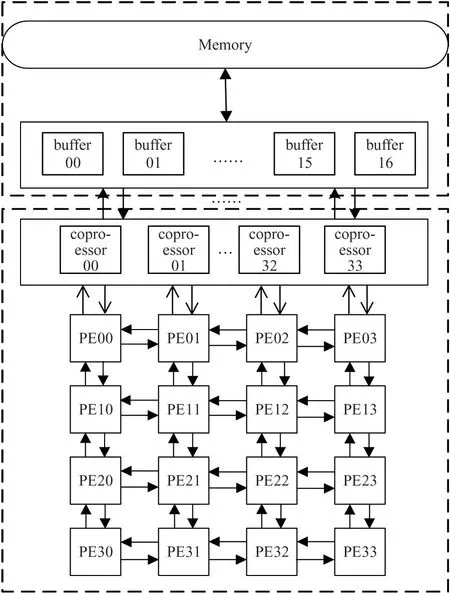
Fig.1 Near-memory computing architecture based on reconfigurable array processor
Without changing the programming interface of the original reconfigurable architecture,the near-memory computing array integrates with the reconfigurable array processor through custom instructions.The key part of the reconfigurable array are the process elements group(PEG),each PEG contains 4×4 process element PE,16 PEs are connected topologically through adjacency and interconnection of shared registers,and each PE is realized based on reduced instruction set computer(RISC)architecture.Each PE in the reconfigurable array is used as the main processor.The calculation and memory access modes are switched in real-time according to memory access requirements.The PE array can access the local memory directly,and can also issue a near-memory computing instruction to the coprocessor to perform simple calculations on the main memory.
2.1 Near-memory computing array
The key part of the near-memory computing array is 16 coprocessors,and each coprocessor has a one-toone correspondence with the main processor.When the main processor PE receives the configuration information issued in real-time through the H-tree configuration network[15],it sends the instructions to the coprocessor through the communication interface with the coprocessor.Before the coprocessor executes the instructions,the operation code represented by the high 6 bit of the instruction is used as a flag to determine whether the currently issued instruction is a calculation instruction supported by the coprocessor.If the opcode of the current instruction does not point to the coprocessor,the instruction is executed in the main processor and the coprocessor does not work.Otherwise,the instruction information of the current instruction except the high 6 bit opcode is issued to the coprocessor for execution.
According to the characteristics of convolutional calculation,the near-memory computing instructions are specially designed with the characteristics of storecalculation integration,which can support the calculation of fetching from the memory and the update of the data in the memory.The data does not need to be transmitted to the PE array through multi-level buffering for calculation,which speeds up the calculation process of the CNN.
Table 1 lists some of the special instructions supported by the coprocessor.Among them,M[Rs]and M[Rt]indicate that the source operand comes from external memory,and M[Rd]indicates that the result of the operation is written back to the memory.To further improve the calculation speed of the CNN algorithm,according to the calculation characteristics of the convolution operation in CNN,the multiplication and accumulation instruction MAC and the accumulation register Rm are designed.The input image pixels from the external storage are multiplied by the weight in the convolution kernel and directly added.The calculation result of the previous convolution stored in the register is accumulated,and the result is read from Rm by executing the STRM2 instruction,and the accumulation register is cleared in the next clock cycle after the result is read.
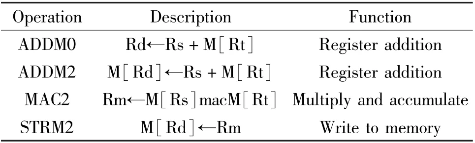
Table 1 Some special instructions supported by the coprocessor
To improve the efficiency of algorithm processing,a three-stage pipeline architecture is adopted in the coprocessor unit as shown in Fig.2.Buffering instruction,decoding and fetching data,execution and writeback are corresponding to the three levels respectively.The first level is used to buffer the calculation instructions issued by the main processor.The second level is used to decode instructions and obtain the source operands required for instruction execution according to the decoding results.The main function of the third level is to execute instructions and write the execution result of the instruction back to the destination address.
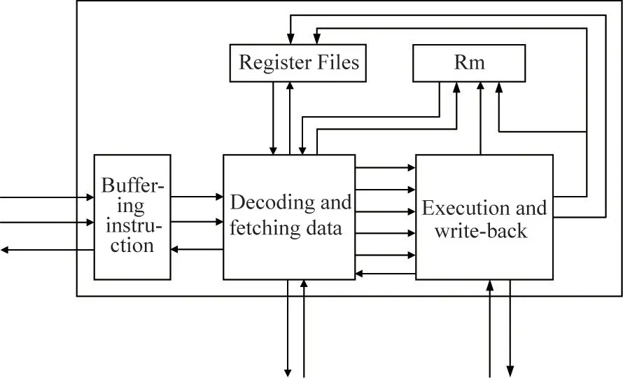
Fig.2 The architecture of coprocessor
2.2 Shared buffer array
Near-memory computing arrays have the characteristics of high parallelism,and the use of traditional shared storage structures will have problems such as large access conflicts.The continuous sliding of the convolution window during the CNN processing will cause the data in the main memory to be frequently accessed,resulting in a large memory access overhead.Therefore,in order to reduce the data communication between the near-memory computing array and the main memory,an array-type shared buffer array storage structure is proposed.At the same time,the array-type storage structure can further improve the parallel access of the near-memory computing array.Since each coprocessor in the near-memory computing array can access the main memory,at least 16 buffer units are used.At the same time,considering that the convolution kernel is used in the convolution calculation of the entire feature image,the global reusability is higher,and the weight of the convolution kernel needs to be buffered in the buffer unit.Therefore,the designed shared cache array consists of 17 buffers that support non-aligned storage access.
The entire shared buffer array is mainly composed of a judge unit,17 buffer units(buffer00-buffer16)and an arbiter,as shown in Fig.3.When the coprocessor sends an access request,it is first received by judge unit to determine whether the access is hit.If it is hit,the request will be sent to the corresponding hit buffer to directly read or update the data in the destination buffer.If it is not hit,it will be arbitrated to access the main memory.Each buffer is composed of a tag register unit and a data buffer unit.The tag register unit is used to store the state of the buffer unit and the first address of the buffered data.If the write access hits,the dirty location is to be set while updating the data.
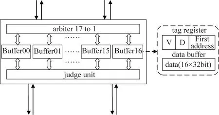
Fig.3 Shared buffer array structure
3 CNN parallel mapping
3.1 Alex Net
CNN can be used to construct hierarchical classifiers[16],and can also be used in fine-grained recognition to extract discriminative features of images for learning by other classifiers[17].Based on the hardware platform architecture of the near-memory computing array and the shared buffer array,the parallel mapping of the AlexNet is completed and it conducts test verification and performance analysis on the proposed architecture.The specific structure of the AlexNet is shown in Table 2.
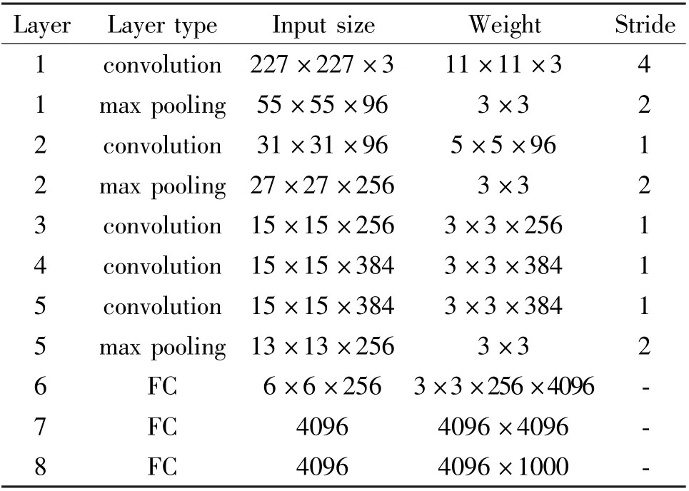
Table 2 Specific structure of AlexNet
Table 3 shows the calculation complexity and memory occupancy of the network model of each type of AlexNet network[18].From the table,it can be seen that the total amount of data of AlexNet network model parameters is very large,which can reach 230 MB.It is far more than on-chip memory capacity,so all parameters can only be stored in off-chip memory.When classifying and identifying a frame of the input feature map,the convolution operation process in CNN will consume plenty of computational resources,and about 1.33 GOPs are required in the AlexNet.Among all sub-network layers,the convolutional layer is the most computationally intensive part,accounting for more than 90% of the total computational amount of the entire network.

Table 3 AlexNet network scale analysis
3.2 Parallel mapping
According to the structural characteristics of the near-memory computing array and the potential parallelism of CNN,a parallel mapping method is proposed.All memory access computing instructions will be executed in the coprocessor,and the main processor mainly controls the loop in the convolution operation.In this way,the parallelism of the CNN calculation can be improved,and the calculation efficiency of the processor can be promoted.
In the AlexNet,the convolutional layer includes three types of 11×11,5×5,and 3×3[19].The parallel mapping method to implement the convolution operation is as follows.
(1)When the size of the convolution kernel is 11×11,the input image size is 227×227.PE00-PE22 respectively completes the 1×11 convolution calculation,and PE30 accumulates the intermediate calculation data of these eleven PEs to obtain the final convolution result.
After the instruction is issued and the operands required for the calculation instruction are ready,PE00 starts to do the 1×11 multiply-accumulate operation in the first line of the input image,and PE01 does the 1×11 multiply-accumulate operation in the second line,and so on.PE00-PE22 will send a handshake signal to PE30 after completing a 1×11 convolution.When PE30 receives the handshake signal,it will read out the eleven convolution results of PE00-PE22 and accumulate them.Then,it is stored in the corresponding memory location,and PE30 will also send a handshake signal to eleven PEs to indicate that the reception is complete.When PE00-PE22 receives the handshake signal of PE30,they will slide the convolution window to the right and continue to do the next 11×11 convolution until all the convolution results of this layer are obtained.The mapping structure is shown in Fig.4.
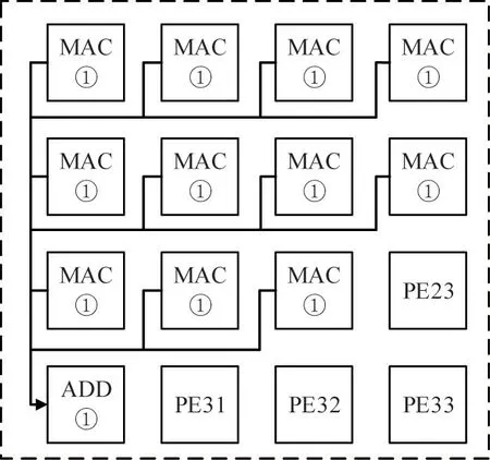
Fig.4 11×11 convolution operation map
(2)When the size of the convolution kernel is 5×5,the input image size is 27×27.PE00-PE10 respectively completes the 1×5 convolution operation,and PE30 accumulates the intermediate calculation data of five PEs to obtain a 5×5 convolution result.At the same time,after PE11-PE21 respectively completes the 1×5 convolution operation,they send the result to PE31 for accumulation and output a 5×5 convolution result.
After the instruction is issued,PE00 does the 1×5 multiplication and accumulation operation of the first line of this layer of input,PE01 does the 1×5 multiplication and accumulation operation of the second line of the input image,and so on.At the same time,PE11-PE21 will multiply and accumulate lines 2 to 6 of the input image of this layer.Take PE00-PE10 convolution and accumulation in PE30 as an example:after PE00-PE10 completes a 1×5 convolution,they will send handshake signals to PE30 respectively.When PE30 receives the handshake signals,it will read out the intermediate calculation data of five PEs and write them back to the main memory after accumulation.PE30 will also send handshake signals to PE00-PE10 to indicate that the reception is complete.When PE00-PE10 receives the handshake signal of PE30,they will slide the convolution window to the right and continue to do the next 5×5 convolution until all results are obtained.The mapping structure is shown in Fig.5.
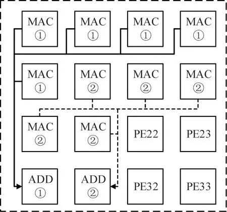
Fig.5 5×5 convolution operation map
(3)When the size of the convolution kernel is 3×3,the input image size is 15×15.PE00-PE02 completes the 1×3 convolution operation respectively,and PE30 accumulates the intermediate calculation data of 3 PEs to obtain a 3×3 convolution result.At the same time,PE03-PE11 respectively completes the 1×5 convolution operation,sends the result to PE31 for accumulation and outputs a 3×3 convolution result.PE12-PE20 respectively completes 1×3 convolution operations and PE30 performs accumulation to obtain a 3×3 convolution result.
When the instruction is issued,PE00 will start the 1×3 multiplication and accumulation operation of the first line of the input image,PE01 will do the 1×3 multiplication and accumulation operation of the second line of the input image,and PE02 will do the third line of the input image.PE03-PE11 will do 1×3 multiply and accumulate operations from rows 2 to 4 at the same time,while PE12-PE20 will do 1×3 from rows 3 to 5 multiply and accumulate operations.Take PE00-PE02 convolution and accumulate in PE30 as an example:when PE00-PE02 completes a 1×3 convolution,they will send handshake signals to PE30,and when PE30 receives the handshake signals,it will read intermediate calculation data of PE00-PE02,sum this data and write back the result to the corresponding memory location.Meanwhile,PE30 will send handshake signals to these PEs to indicate that the reception is complete.When PE00-PE02 receives the handshake signal of PE30,they will slide the convolution window to the right and continue to do the following 3×3 convolution until all the results are obtained.The mapping structure is shown in Fig.6.
Fig.6 3×3 convolution operation map
3.3 Data reuse analysis
The shared buffer array is used to buffer data to realize data reuse.Take the convolution operation of 3×3 size as an example,as shown in Fig.7.When the size of the convolution kernel is 3×3,twelve coprocessors are used to process three 3×3 convolution operations at the same time,of which nine coprocessors are used to perform 1×3 convolution operation,and three coprocessors are used to accumulate intermediate calculation data.When twelve coprocessors perform calculations at a time,twelve buffer units are required.Because the 3×3 convolution operation stride is one,each buffer unit can buffer sixteen 32-bit data of consecutive addresses.Therefore,when the convolution window slides to the right,if the buffer is hit,the data of the destination address can be directly read or updated,which extremely improves the data reuse of the convolution process and reduces the data communication between the near-memory computing array and the main memory.It also reduces the memory access latency and overhead.The occupancy of 5×5 and 11×11 convolution buffers is similar,but compared with 5×5 and 11×11 convolutions,the data reuse rate with the 3×3 convolution operation is the highest.
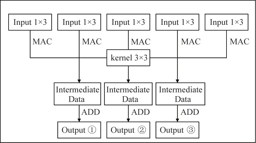
Fig.7 3×3 convolutional data reuse situation
4 Experimental results and analysis
Xilinx’s Virtex 6 field programmable gate array(FPGA)development board is chosen to verify the proposed architecture and AlexNet CNN is realized on it.The source occupation can be seen in Table 4.The working frequency on FPGA is 110 MHz.
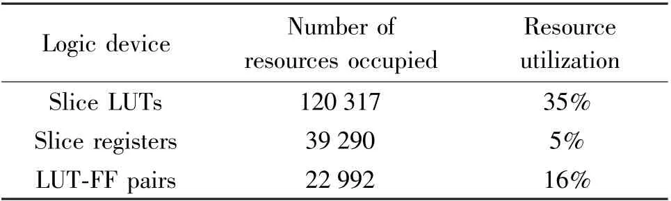
Table 4 Hardware resource usage
The computing time of single convolution is counted as shown in Table 5.Compared with Ref.[20],the performance is improved by 69.60%,75.00%,and 55.32%,respectively.
The execution clock cycle of each layer of the convolutional layer is shown in Table 6.The proposed parallel computing method is used to perform convolution operations in the near-memory computing array architecture based on the reconfigurable array processor,and the designed architecture is verified and tested.In this paper,C1 inputs 3 images and outputs 96 feature maps,C2 inputs 96 feature images,and outputs 256 feature maps.The processing speed of the CNN accelerator proposed in Ref.[21]is faster than this paper.It is because each layer of C1-C5 has 2 input feature maps,and the amount of data processing is much lower than this paper.Comparing in processing single feature maps,this paper is faster than Ref.[21].Ref.[20]based on the multiple parallel features of CNN calculations proposed an architecture of CNN forward propagation process in parallel calculation,but the calculation speed is slower than this article.Ref.[22]used a reconfigurable array processor that does not support near-memory computing.Compared with it,the overall processing speed of the architecture designed in this paper is increased by 8.81%.
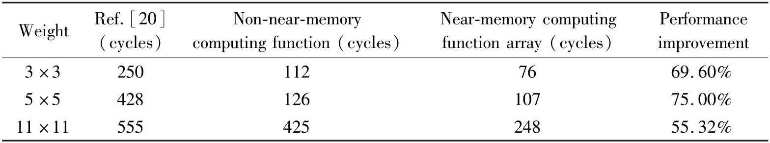
Table 5 Comparison of the consumption time of single convolution

Table 6 Convolutional layer execution time comparison
Ref.[23]proposed a CNN hardware accelerator with an array architecture,which can reconfigure the layer parameters adapt to different CNN structures.By using multiple PEs to perform convolution operations at the same time,the calculation parallelism is improved.And the convolution processing speed is further enhanced.The frequency of the circuit under this architecture can reach 100 MHz.Ref.[24]designed and implemented an efficient and reusable CNN FPGA accelerator.Based on the modified roofline model,the microstructure of accelerator was optimized,the underlying FPGA calculation and bandwidth resource utilization were maximized.But the accuracy of this architecture is lower,and the power consumption is higher than this paper.Ref.[25]proposed a configurable neural network computing architecture by using reconfigurable data quantification to reduce power consumption and on-chip memory requirements,but this architecture is not universal.The maximum frequency of this paper can reach 110 MHz,which is greatly improved compared with Ref.[17]and Ref.[19]and supports 32-bit operand width.Table 7 shows the comparison of frequency,precision and power for different architectures.

Table 7 Comparison of frequency,precision and power
5 Conclusion
For data-intensive applications such as deep learning,a near-memory computing array architecture based on the shared buffer is designed to improve the speed of intensive computing and alleviate bandwidth pressure.The memory occupancy is analyzed,and a method to realize the parallel calculation of the CNN is designed.The experimental results show that the architecture of this paper increases the speed of convolution operation while reducing memory access latency and improving data reuse.The highest frequency can reach 110 MHz.Compared with previous studies,the calculation speed of a single convolution operation is increased by 66.64% on average.Compared with the reconfigurable array processor that does not support near-memory computing,the processing speed of the entire convolutional layer is increased by 8.81%.
杂志排行

High Technology Letters的其它文章
- Adaptive cubature Kalman filter based on variational Bayesian inference under measurement uncertainty①
- Design and experimental study of active balancing actuator driven by ultrasonic motor①
- Trajectory tracking control of characteristic model for nonplanar hex-rotor UAV①
- The adaptive distributed learning based on homomorphic encryption and blockchain①
- HOPE:a heterogeneity-oriented parallel execution engine for inference on mobiles①
- Joint utility optimization algorithm for secure hybrid spectrum sharing①