Structural optimization and performance testing of gold microarray electrode fabricated by DMD lithography and electrodeposition
2022-05-28YANGDongfangLUZifengLIUHuaSHANGuiye
YANG Dong-fang,LU Zi-feng,LIU Hua,SHAN Gui-ye
(Center for Advanced Optoelectronic Functional Materials Research, and Key Laboratory for UV Emitting Materials and Technology of Ministry of Education, National Demonstration Center for Experimental Physics Education, Northeast Normal University, Changchun 130024, China)
Abstract:In order to improve the detection efficiency of Micro Array Electrodes (MAE) and reduce the production cost,a technology combining Digital Micromirror Device (DMD) maskless projection lithography with electrochemical deposition was proposed.Firstly,a user-defined micro array was fabricated by using the advantages of lithography system such as high-resolution PZS motion and imaging flexibility of DMD.And a uniform Au microarray electrode (Au/MAE) was fabricated after obtaining an Au conducting layer by electrodeposition.Then,the electrochemical properties of Au/MAE with different structures were compared by cyclic voltammetry,and the optimized structural parameters were obtained.Finally,the current response of optimized Au/MAE to the glucose with different concentrations and pH values was studied,and the anti-interference of Au/MAE in glucose detection was tested by chronoamperometry.The electrochemical analysis shows that the simple Au/MAE has a significant amperometric response,a strong anti-interference ability and a sensitivity of 101 μA·cm−2·mM−1 in the electrochemical detection of glucose.This method has the advantages of high resolution,high consistency,simple process and low cost,which provides a feasible operation scheme for the fabrication of biosensor array.
Key words:DMD lithography;electrochemical deposition;microstructure array;electrode
1 Introduction
Electrochemical Biosensor Array (EBA) has been widely used in food detection,environmental monitoring,health care and other fields due to its advantages such as high selectivity,high sensitivity and fast analysis speed[1-4].As a signal converter,Micro Array Electrode (MAE) is an important part of EBA,and its performance will directly affect the detection performance of EBA[5-8].However,the fabrication technique of MAE is the basis and key of array electrode research[9-12].The fabrication techniques of microarray electrodes include the following ones.The preparation process based on mask needs to prepare a large number of masks according to different microelectrode structures.In order to realize the optimal design of structural parameters of gold microarray,the design and preparation of the masks need a lot of time and thus have a high cost and poor flexibility[13].The lithography based on etching technology is currently the preferred method for preparing microarray electrodes due to the advantages of good controllability,high precision,good electrode surface flatness and high interbatch reproducibility in preparing planar ordered array electrodes[14].Femtosecond laser direct-writing technology can prepare microelectrode arrays with highresolution graphics,but cannot achieve large-area machining[15].The maskless lithography based on DMD has as many as 2 million micromirrors and each micromirror can be equivalent to an independent light source,so the exposure process is equivalent to the point-to-point exposure of multiple beams.At the same time,the switching frequency of DMD micromirrors matches the running speed of the sample stage,thus realizing the rolling exposure of graphics and the preparation of any periodic structural array.Compared with femtosecond laser direct-writing system,the maskless lithography technology based on DMD has much higher production efficiency and lower fabrication cost.
We combined the DMD maskless multi-step lithography system built by our research group with electrochemical deposition technology to prepare a user-defined micro-structure array[16-19].Indium Tin Oxides (ITO) conducting glass is widely used in the field of electrochemistry because of its excellent properties such as low resistivity,high conductivity and good machining performance.Therefore,with ITO conducting glass as substrate,many periodic and aperiodic MAEs with various shapes were prepared by using the combined machining techniques(including flexible DMD patterning,multi-step lithography and dose modulation technique),designing the mask patterns and controlling the lithography process parameters (exposure time and exposure energy).Then,electrochemical deposition technique was used to uniformly deposit Au onto the prepared microstructural array template to obtain various periodic and aperiodic Au microarray electrodes (Au/MAEs) with arbitrary shapes.The electrochemical properties of the MAEs with different structures were compared and analyzed,and the influence of shape,period and surface area on the REDOX peak current was systematically studied.The Au/MAE structure prepared with the total surface area unchanged and a cell surface area of 1.7×10⁻⁵cm2had a higher REDOX peak current.The structural parameters of Au/MAE were optimized.In addition,the distance between adjacent cell structures was minimized to prepare the Au/MAEs with densely arranged cells which could be used for glucose detection.The sensitivity of this Au/MAE was determined as 101 μA·cm−2·mM−1through testing its glucose-detecting performance and anti-interference performance,thereby demonstrating the feasibility of this MAE preparation method.
2 Principle and method of Au/MAE preparation
2.1 DMD projection lithography system and electrochemical deposition experiment setup
Fig.1(a) shows a maskless projection lithography system based on DMD.The DMD (Texas Instruments) consists of an array of 1 024×768 micromirrors.The side length of each micromirror is 1 pixel,that is 1.368 μm.The piezoelectric stage (PZS) can move slightly alongXandYdirections in horizontal plane.Its motion range is 100 μm×100 μm,and its displacement accuracy is up to 7 nm.After the beam expansion and collimation,the LED light source with a central wavelength of 385 nm is incident on DMD at a certain angle to the optical axis of the optical system.The pre-designed pattern is input into DMD chip by computer through the corresponding software.The light beam reflected by DMD carries the image information.Through the projection objective with a minification of 10,the beam is finally focused on the substrate (ITO),which is spin-coated with positive photoresist (S1318) and placed on the PZS.Finally,the loading of a digital mask onto DMD and the high-precision PZS motion is synchronously controlled by computer to realize multi-step lithography.

Fig.1 (a) Schematic diagram of maskless projection lithography system based on DMD and (b) experimental setup of electrochemical deposition图1 (a) 基于DMD 的无掩模投影光刻系统示意图;(b) 电化学沉积的实验装置图
Fig.1(b) shows the experimental setup of electrochemical deposition,which mainly includes three-electrode system (working electrode,reference electrode and auxiliary electrode),electrolytic bath,electrolyte,potentiostat,etc.In this experiment,Ag/AgCl was used as the reference electrode,a platinum wire was used as the auxiliary electrode,and an ITO substrate engraved with a microstructural array was used as the working electrode.HAuCl4solution and KCl solution (volume ratio:4∶5) was used as electrolyte.Au nanoparticles were electrodeposited for a certain time under a certain voltage to prepare an Au conducting layer.
2.2 Preparation process of Au/MAE
We combined digital multi-step lithography(DMSL) with electrochemical deposition technique to prepare Au/MAE with ITO as the substrate.The specific experimental process is shown in Fig.2(coler online).Fig.2(a) shows the substrate pretreatment process,that is,washing the ITO glass substrate with acetone,anhydrous ethanol,distilled water and ultrasound successively and then drying it in a nitrogen flow.Fig.2(b) shows the spincoating and pre-drying process of photoresist,which is to apply positive photoresist evenly on the substrate with the aid of a pipette,spin-coat it on ITO glass at a certain speed to obtain a certain thickness of photoresist layer,and then bake the photoresist layer for 10 min on a 95℃ hot plate to remove residual solvent,improve the photoresist sensitivity and make it solidify.Fig.2(c) shows the maskless lithography and development process based on DMD,which is to expose photoresist to the pre-designed mask pattern through DMD lithography system,develop it in 5‰ NaOH solution for a certain time,and then remove the exposed photoresist.Fig.2(d) shows the electrochemical deposition process of Au nanoparticles,which is to use 0.1 M HAuCl4·4H2O and 0.1 M KCl solution(Volume ratio of HAuCl4∶KCl is about 1∶1) as electrolyte,deposit it for a certain time under a certain voltage,and then wash and remove the unexposed photoresist with acetone and distilled water successively to obtain the MAE structure as shown in Fig.2(e).
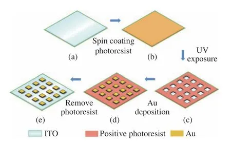
Fig.2 Flow chart of Au/MAE preparation process.(a) Substrate pretreatment;(b) photoresist spin-coating and pre drying;(c) exposure and development;(d) electrochemical deposition of Au nano layer;(e) photoresist removal图2 Au/MAE 的制备流程图。(a) 基片预处理;(b) 旋涂光刻胶和前烘;(c) 曝光并显影;(d) 电化学沉积Au 纳米层;(e) 去除光刻胶
2.3 Au/MAE preparation
A series of MAEs was prepared by DMSL (exposure time:3 s,exposure energy:145 mJ/cm2),Au/MAE was obtained by the electrochemical deposition of Au nano-conducting layer,and the images of MAE and Au/MAE were observed under Olympus microscope.Given the same total surface area (3.7×10⁻³cm2) and cell surface area (1.7×10⁻⁵cm2),the circular,hexagonal and triangular microarray structures with periodic arrangement were prepared as shown in Fig.3(a),(b) and (c).The corresponding microscopic images of Au/MAEs are shown in Fig.3(d),(e) and (f).It can be seen that both MAE and Au/MAE have regular shapes,clear edges,smooth lines and good morphology.Similarly,when the total surface area and cell surface area remained unchanged,we prepared the elliptical,hexagonal and five-pointed Au/MAE structures with aperiodic arrangement,as shown in Fig.4.By using the combination of dose modulation and DMSL,the user-defined MAEs can be fabricated.

Fig.3 Results of periodic structures.The actual exposure and electrodeposition results of MAE and Au/MAE structures of circular ((a) and (d));hexagonal ((b) and (e))and triangular ((c) and (f)) under optical microscope图3 周期性结构测试结果。圆形 ((a) 和 (d)) ;六边形 ((b) 和 (e)) 以及三角形 ((c) 和 (f)) 的MAE 和Au/MAE 在光学显微镜下的实际曝光和电沉积结果
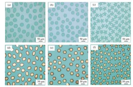
Fig.4 Aperiodic structures results.The actual exposure and electrodeposition results of MAE and Au/MAE of elliptical ((a)and (d));hexagonal ((b) and (e)) and five-pointed ((c) and (f)) under optical microscope图4 非周期性结构结果。椭圆形((a)和(d));六边形((b)和(e))以及五角星((c)和(f))的MAE 和Au/MAE 在光学显微镜下的实际曝光和电沉积结果
3 Optimization of Au/MAE structure parameters
Since the height of the prepared MAE cell structure was negligible compared with its surface width,the influence of MAE cell area and density on the electrode performance was investigated.The electrochemical response of the Au/MAEs with different cell shapes in PBS buffer solution (pH 7.0)was investigated by cyclic voltammetry at a scanning rate of 100 mV/s within a potential range of 0−1.4 V.
First,the electrochemical performance of the Au/MAEs with different shapes was studied when the cell surface area was 5.9×10⁻⁶cm2,8.3×10−6cm2,1.7×10−5cm2or 3.3×10⁻⁵cm2,and the total surface area remained unchanged (3.7×10⁻³cm2).The cyclic voltammetry (CV) curves of circular,hexagonal and triangular structures with periodic arrangement are shown in Fig.5(a),(b) and (c).It can be seen from Fig.5 (color online) that the Au/MAEs with the same cell shape but different cell areas and with the same total surface area will have different REDOX peak currents.By comparing the three structures,it is found that although they have different cell shapes,their CV currents change in the same way,that is,to increase first and then decrease with the increase of cell structure area.This is because the REDOX peak current is closely related to the number of REDOX contact sites and the strength of signal transmission in microarray structure.When the surface area of a cell structure increases from 5.9×10⁻⁶cm2to 3.3×10⁻⁵cm2and the total surface area remains unchanged,the number of cell structures will decrease to so that the number of contact sites will decrease and the REDOX peak value will drop.On the other hand,the presence of fewer cell structures will result in the reduction of Au/MAE resistance and the increase of REDOX peak current.Under the competition of these two factors,the peak current will show a change trend of first increasing and then decreasing,instead of linear change.When the cell area is 1.7×10⁻⁵cm2,the peak current in both oxidation and reduction will be the highest.Then,with the total surface area unchanged,the Au/MAE structures with different shapes and random arrangement were prepared according to the above experimental parameters,and the electrochemical performance of each Au/MAE structure was tested.The CV curves of elliptical,hexagonal and five-pointed structures with aperiodic arrangement are shown in Fig.5(d),(e) and (f) respectively.It can be seen that for the same aperiodic structure,the REDOX peak current will also increase first and then decrease with the increase of cell surface area when the total surface area remains unchanged.This analysis shows that the total area and cell area are also the main factors affecting the electrochemical performance of an Au/MAE structure with random arrangement,which is consistent with the experimental conclusion obtained above.
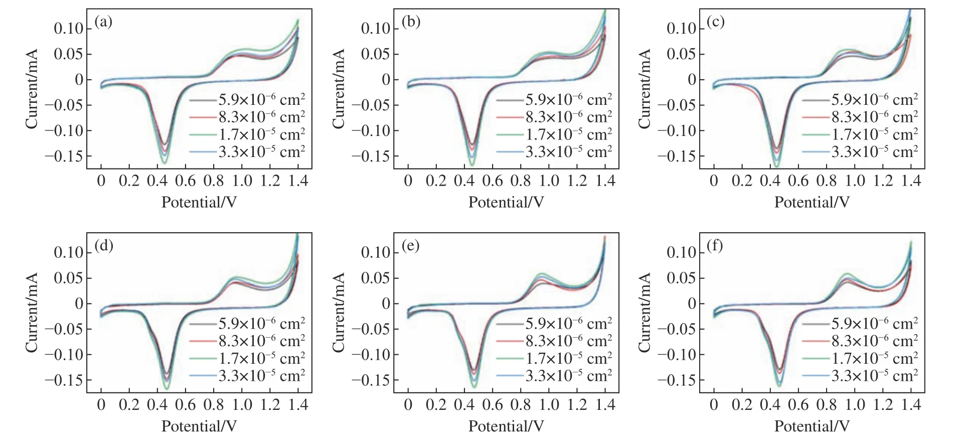
Fig.5 Effect of cell surface area on REDOX peak current under the same total surface area.CV diagrams of (a) circular;(b)hexagonal and (c) triangular Au/MAE structures with periodic arrangement and of (d) elliptical;(e) hexagonal and (f)five-pointed Au/MAE structures with aperiodic arrangement图5 总表面积不变,单元表面积对氧化还原峰电流的影响,周期性排列的(a)圆形;(b)六边形;(c)三角形以及非周期性排列的(d)椭圆;(e)六边形;(f)五角星结构的Au/MAE 的CV 图
It can also be seen from Fig.5 that when both the total surface area and the cell area remain unchanged,the CV current results of Au/MAE structures with periodic or aperiodic arrangement and different cell shapes will be basically the same.In summary,it can be concluded that the REDOX peak current value of Au/MAE structures is closely related to the total surface area and cell structure area,and has nothing to do with cell structure shape.
The Fig.6(a) shows the relationship between the value of oxidation peak current and the surface area of electrode cell structure when the total surface area is constant.As can be seen from the figure,with the increase of cell surface area,the oxidation peak will first increase and then decrease.The curves of the circular,square and hexagonal structures basically coincide,indicating that the oxidation peak current is independent of the cell shape when the total surface area and the cell surface area remain constant.The Fig.6(b) shows the oxidation peak current of a square Au/MAE structure with different cell surface areas as a function of the total surface area.It can be seen that when the cell surface area is constant,the value of oxidation peak current will increases linearly with the increase of the total surface area.
From the above analysis,it can be seen that the main factors affecting the electrochemical performance of Au/MAE are the total surface area and the cell surface area,rather than cell shape.Based on this,we optimized the structural parameters of Au/MAE,that is,the cell surface area (1.7×10⁻⁵cm2)producing the optimal REDOX peak current was selected when the total surface area was constant(3.7×10⁻³cm2).In addition,by minimizing the spacing between two adjacent cell structures,an Au/MAE with densely arranged square cells was prepared,and its performance was tested.
4 Evaluation of Au/MAE performance
4.1 Electrochemical performance of Au and Au/MAE electrodes
According to the optimized parameters obtained from the above study,we prepared the Au/MAE with densely arranged square cells.The cell surface area was 1.7×10⁻⁵cm2,and the actual spacing between adjacent cell structures was 1.26 μm.The Fig.7(a) (color online) and Fig.7(b)(color online) respectively show the optical microscope images of the MAE and Au/MAE with densely arranged cells,whose spacing is about 1.26 μm.When the spacing is reduced to 1 pixel (1.368 μm),the gold nanoparticles will spread outward during electrodeposition,resulting in a smaller spacing that cannot be distinguished.Therefore,when the spacing of the design pattern structures is 2 pixels,the microarray composed of square cell structures with this spacing is the densest.The Fig.7(c) (color online) and Fig.7(d) (color online) give the optical microscope images of Au/MAE in full exposure and of single Au electrode respectively.The electrochemical properties of single Au electrode and Au/MAE were compared by cyclic voltammetry.
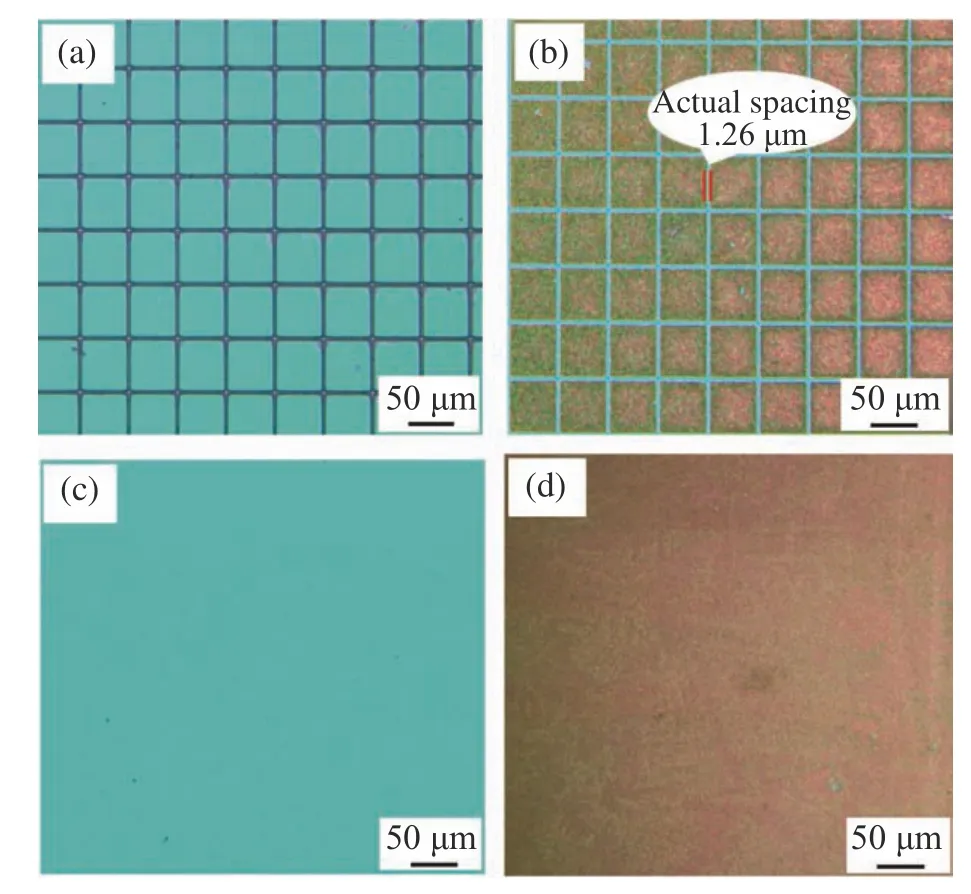
Fig.7 (a) Microscope image of the MAE with the most densely arranged cells;(b) microscope image of Au/MAE after electrodeposition;(c) microscope image obtained after full exposure;(d) microscope image of single Au electrode after electrodeposition图7 (a) 密集排列的MAE 的显微镜图像;(b) 电沉积后的Au/MAE 的光学显微镜图;(c)全部曝光后的显微镜图像;(d)电沉积后的单个Au 电极光学显微镜图
Fig.8 (color online) shows the CV curves of Au electrode and Au/MAE obtained before and after adding 2 mM glucose to 0.1 mM PBS buffer solution (pH 7.0).Before glucose was added (Fig.8(a)),Au electrode had basically no current response.In contrast,Au/MAE had an obvious REDOX peak.After 2 mM glucose was added (Fig.8 (b)),REDOX peaks appeared at the 0−1.4 V scanning potential for both Au electrode and Au/MAE.The peak pair appearing at the voltages of 0.97 V and 0.44 V was the REDOX peak of Au nanoparticles.Compared with Au electrode,Au/MAE showed good electrochemical response.The obtained oxidation peak current was about 6 times that of Au electrode,indicating that Au/MAE had a higher electrochemically-active specific surface area.

Fig.8 Comparison of electrochemical performance between Au electrode (a) and Au/MAE (b)图8 Au 电极(a)与Au/MAE 电极(b)电化学性能比较
4.2 Glucose detection by Au/MAE
Compared with Au electrode,the optimized Au/MAE showed obvious current response with or without the presence of glucose.This confirmed that the prepared electrode had good electrochemical performance and played an important role in the electrochemical oxidation of glucose.Therefore,this electrode can be applied to the research of glucose sensing and the further electrochemical detection of glucose.The effect of Au/MAE on the oxidation of glucose (concentration:1 mM) at different scanning rates (10−1 000 mV/s) was studied to obtain the results as shown in Fig.9(a) (color online).The REDOX peak current increases with the scanning speed,the anodic peak moves slightly from 0.95 V to 1.04 V,and the cathodic peak moves from 0.48 V to 0.39 V.Therefore,the electrode is highly sensitive to glucose oxidation.In Fig.9(b) (color online),the obtained anodic and cathodic peak currents versus scanning speed were plotted and fitted.It can be seen from the figure that with the increase of scanning rate from 10 mV/s to 1 000 mV/s,the absolute value of REDOX peak current will increase linearly,and the linear fitting regression coefficients of cathodic and anodic peaks will be 0.997 and 0.994 respectively (ifR2is closer to 1,the fitting will be better).According to the electrochemical theory,the peak current is directly proportional to the scanning speed in the electrode reaction process controlled by surface adsorption.The ratio of anodic peak current to cathodic peak current is close to 1.These typical characteristics indicate that the electron transfer process on Au/MAE electrode is controlled by surface adsorption.
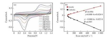
Fig.9 For Au/MAE (glucose concentration:1 mM) in 0.1 mM PBS (pH 7.0) buffer solution,(a) CV diagram at different scanning rates (10−1 000 mV/s);(b) fitting diagram of anodic and cathodic peak currents at different scanning rates图9 Au/MAE 在含有1 mM 葡萄糖的0.1 mM PBS(pH 7.0)缓冲溶液中,(a)不同扫描速度下 (10−1 000 mV/s) 的CV 图以及(b)不同扫描速率下的阳极和阴极峰值电流拟合图
The above experiments verify the ability of Au/MAE to sense glucose,so the prepared Au/MAE can be used as a non-enzymatic glucose-sensing electrode.The electrochemical response of Au/MAE to different glucose concentrations was studied when the scanning rate was 100 mV/s.Fig.10(a)(color online) shows the linear voltammetry curves of Au/MAE in PBS (0.1 mM,pH 7.0) at different glucose concentrations.It can be seen that the Au/MAE oxidation/reduction peak currents increase with the increase of glucose concentration from 1 mM to 8 mM.The corresponding standard curve is shown in Fig.10(b).It can be seen that within the whole concentration range,the response of Au/MAE to glucose concentration satisfies a linear relationship.To determine the sensitivity and response time of Au/MAE as a glucose sensor,we measured the amperometric response of Au/MAE to the continuous addition of glucose to 0.1 mM PBS while keeping the potential at +0.5 V.It can be seen that the electrode has a fast current response to glucose and can reach a stable current density within 5 s.With the addition of the glucose with different concentrations,the baseline of the curve will drift slightly (as shown in Fig.10(c)),because the consumption rate of glucose on the electrode surface is faster than its diffusion rate,or because the midbody is adsorbed to the active site.The fitting curve of the glucose sensor is shown in Fig.10(d),indicating that Au/MAE peak current has a linear relationship with the glucose concentration in the range of 0.01 mM−1 mM (R2=0.986).The sensitivity calculated according to the standard curve is 101 μA·cm−2·mM−1.This proves that Au/MAE has excellent glucose-sensing performance.
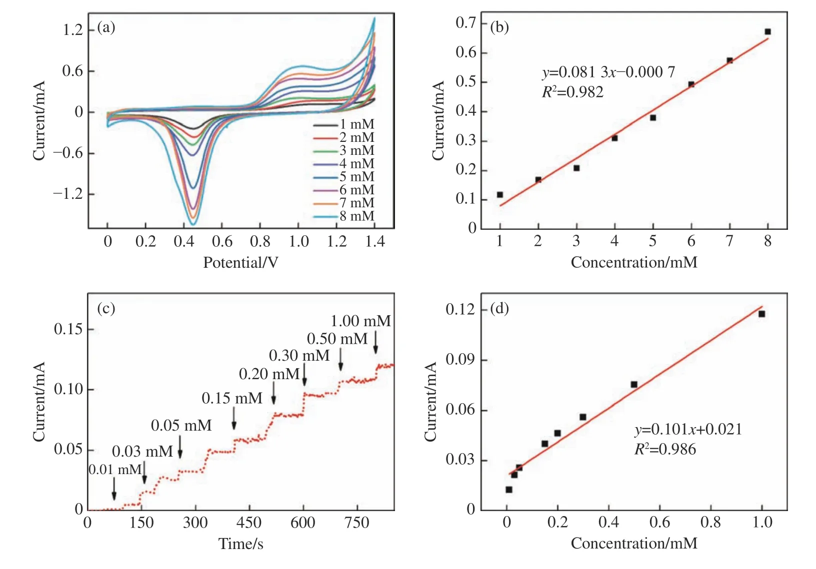
Fig.10 (a) Cyclic voltammograms of Au/MAE electrode at different glucose concentrations in 0.1 mM PBS (pH 7.0) (scanning rate:100 mV/s) and (b) the corresponding calibration curve;(c) amperometric response of Au/MAE electrode to the continuous addition of glucose to 0.1 mM PBS at the voltage of 0.5 V and (d) the corresponding fitting curve图10 0.1 mM PBS (pH 7.0) 条件下,(a) 葡萄糖浓度不同时Au/MAE 的循环伏安图(扫描速率100 mV/s)及(b) 相应的校准曲线;(c) Au/MAE 在0.5 V 电压下,0.1 mM PBS 中连续加入葡萄糖时的安培响应;(d) 对应的拟合曲线
The electrochemical catalytic behavior of Au/MAE on glucose is provided by Au nanoparticles,and the process of generating current response marks the formation of active gold oxide[20].This can be explained by the following equations:
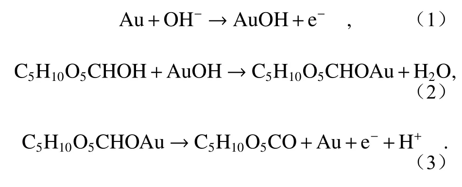
Glucose reacts with the active gold oxide formed in Equation (1) and then is oxidized into glucolactone.
4.3 Anti-interference test of Au/MAE
By testing the anti-interference of Au/MAE against common substances in serum,such as urea and ascorbic acid,we can determine whether the prepared electrode can be used for the practical detection of glucose in serum.By using the chronoamperometry,we studied the current response of the electrode to glucose and other anti-interference substances at 0.5 V voltage,as shown in Fig.11(a).As can be seen from the figure,when 1.5 mM glucose is added,the current will respond rapidly and produce an obvious current signal (close to 0.1 mA).After the interfering substances (uric acid,ascorbic acid,lactose and NaCl) were added in sequence over time,the change of current signal was very small and almost negligible.With further addition of 6 mM glucose,the current signal changed significantly again (up to 0.5 mA).It can thus be seen that the current signal of the electrode is greatly influenced by glucose concentration and has nothing to do with other substances.This may be because Au/MAE surface has a good adsorption effect on glucose molecules,and the electrooxidation effect of glucose molecules is higher than that of lactose,ascorbic acid and other coexisting substances.The Fig.11(b) shows the percentage of the signals of other interfering substances compared to glucose.With glucose signal as reference,the signal percentage of other substances is as small as less than 8%.Obviously,the common substances in blood will not significantly affect the detection of glucose by the electrode,indicating that the electrode has a good selectivity for the amperometric detection of glucose.Therefore,it is proved that Au/MAE bioelectrode has strong anti-interference ability and can be used for the detection of glucose in actual serum.

Fig.11 (a) Amperometric response of the electrode to the continuous addition of 1.5 mM glucose,1 mM urea,1 mM AA,1 mM lactose,1 mM NaCl and 6 mM glucose to PBS (0.1 mM,pH 7.0) buffer solution at 0.5 V voltage;(b) the percentage of interfering signals compared with the target analyte图11 (a) 0.5 V 电压下,在PBS(浓度0.1 mM,pH 7.0)缓冲溶液中连续添加1.5 mM 葡萄糖、1 mM Urea、1 mM AA、1 mM 乳糖、1 mM NaCl 和6 mM 葡萄糖时,电极的安培响应;(b) 与目标分析物相比,相应的干扰信号的百分比
5 Conclusion
Any periodic or aperiodic Au/MAE can be successfully prepared on ITO substrate by combining DMD photolithography with electrochemical deposition.The cyclic voltammetry test shows that the REDOX performance of Au/MAE is related to the area of each structural cell.When the total surface area remains unchanged,the REDOX peak current of a periodic or aperiodic Au/MAE will first increase and then decrease with the increase of cell area,independent of the cell shape.The Au/MAE with dense cell arrangement was prepared by optimizing the structural parameters of the electrode,and then the electrode performance in glucose detection was evaluated.The experimental results show that the electrode has strong catalytic activity and interference resistance in the detection of glucose,with a sensitivity of 101 μA·cm−2·mM−1.It can be used as a non-enzymatic glucose sensor.With the advantages of simple and rapid operation,low cost and high repeatability,this MAE-preparing method can be widely used.
——中文对照版——
1 引言
阵列电化学生物传感器 (Electrochemical Biosensor Array,EBA) 凭借其高选择性、高灵敏度、分析速度快等优点而被广泛应用在食品检测、环境监测、医疗卫生等领域[1-4]。作为信号转换器的微阵列电极 (Microarray electrodes,MAE)是EBA的重要组成部分,其性能将直接影响EBA 的检测性能[5-8]。而微阵列电极的制作技术是阵列电极研究的基础和关键[9-12]。微阵列电极的制作技术包括以下几种:基于掩模板的制备工艺因为需要依据不同的微电极结构制备大量的掩模板,若要实现对金微阵列结构参数的优化设计,掩模板的设计和制备需耗费大量时间,因此成本高、灵活性差[13];而基于刻蚀技术的光刻法,在制备平面有序阵列电极方面具有可控性好、精密度高、电极表面平整度好、批间重现性高等优点,是目前制备微阵列电极的首选方法[14];飞秒激光直写技术虽然可以实现高分辨率图形的微电极阵列的制备,但是无法实现大面积的加工[15];基于数字微镜器件(Digital-Micromirror-Device,DMD)的无掩模光刻技术中,DMD 的微反射镜数目多达200 万个,并且每一个微反射镜都可以等效为一个独立的光源,因而其曝光过程相当于多光束逐点曝光,同时DMD 微反射镜的开关频率与样品台的运行速度相匹配,可实现图形的滚动曝光和任意周期与结构阵列的制备。与飞秒激光直写系统相比,大大提高了系统的生产效率,降低了制作成本。
利用本课题组自行搭建的DMD 无掩模多步光刻系统,结合电化学沉积技术,制备了用户可自定义的微结构阵列[16-19]。氧化铟锡(ITO)导电玻璃具有较低的电阻率、高的导电性能以及加工性能好等优异特性,被广泛应用于电化学领域。因此,以ITO 导电玻璃作为基底,利用复合加工技术(包括DMD 的灵活的图案生成,多步光刻技术和剂量调制技术),通过设计掩模图案并控制光刻工艺参数(曝光时间与曝光能量),制备了各种形状、任意周期以及非周期的微结构阵列(MAE)。再结合电化学沉积技术 (electrochemical deposition technique),将Au 均匀沉积在所制备的微结构阵列模板上,以获得任意形状、周期以及非周期的金微电极阵列 (Au/MAE) 。比较分析了不同结构微电极阵列的电化学性能,系统研究了形状、周期以及表面积等参数对氧化还原峰电流的影响,得知,在总表面积不变,单元结构表面积为1.7×10⁻⁵cm2时制备的Au/MAE 结构具有较高的氧化还原峰电流,接着,优化了Au/MAE 的结构参数,并将相邻单元结构间的距离降低为最小,制备了密集排列的可用于葡萄糖检测的Au/MAE。通过该Au/MAE 对葡萄糖的检测性能和抗干扰性能进行测试,得到的灵敏度为101 μA·cm−2·mM−1,验证了这种阵列电极制备方法的可行性。
2 Au/MAE 的制备原理和方法
2.1 DMD 投影光刻系统与电化学沉积实验装置
图1 (a) 所示是基于DMD 的无掩模投影光刻系统示意图,所用DMD (Texas Instruments) 由1 024×768 个微镜阵列构成,微镜单元的边长为一个像素的大小,即1.368 μm。压电平台 (Piezoelectric stage,PZS) 可在水平面内沿X、Y方向发生微移动,运动范围为100 μm×100 μm,位移精度可达7 nm。中心波长为385 nm 的LED 光源经过扩束与准直后,与光学系统的光轴成一定角度斜入射到DMD 上,预先设计好的图案由计算机通过相应软件输入到DMD 芯片中,被DMD 反射后的光束携带有图像信息,经缩小倍率为10 的投影物镜最后聚焦在基片上 (ITO),该基片上旋涂有正性光刻胶 (S1318) 并放置于PZS 上。计算机同步控制DMD 加载数字掩模板与PZS 的高精度运动来实现多步光刻。
图1 (b) 所示为电化学沉积实验装置示意图,主要包括三电极系统(工作电极、参比电极、辅助电极)、电解槽、电解液、恒电位仪等。本实验中,将Ag/AgCl 作为参比电极,铂丝作为辅助电极,将刻有微结构阵列的ITO 基板作为工作电极。用HAuCl4溶液和KCl 溶液 (体积比4∶5) 作为电解液,在一定的沉积电压和电镀时间下电沉积Au 纳米粒子,制备Au 导电层。
2.2 Au/MAE 的制备流程
将多步光刻 (DMSL)和电化学沉积技术相结合,以ITO 为衬底,制备了Au/MAE,具体实验过程如图2(彩图见期刊电子版)所示。图2 (a) 所示为基片的预处理过程,即分别用丙酮、无水乙醇、蒸馏水超声清洗ITO 玻璃基板,然后在氮气流中干燥。图2(b) 所示为光刻胶的旋涂与前烘过程,即用移液枪将正性光刻胶均匀涂覆于基板上后,再以一定的转速旋涂于ITO 玻璃上,可得到一定厚度的光刻胶层,接着在95℃的热板上烘烤10 min,以去除残留溶剂,提高光刻胶的灵敏度并使其固化。图2(c) 所示为基于DMD 的无掩模光刻和显影过程,将预先设计好的掩模图形通过DMD 光刻系统对光刻胶曝光后,置于5‰的Na-OH 溶液中显影一定时间,再去除被曝光的光刻胶。图2(d) 所示为Au 纳米粒子的电化学沉积过程,以0.1 M 的HAuCl4·4H2O和0.1 M 的KCl 溶液 (HAuCl4∶KCl 体积比约1∶1) 作为电解液,在一定电压下沉积一定时间后,分别用丙酮和蒸馏水清洗去除未曝光的光刻胶,就可获得如图2(e) 所示图形的微阵列电极结构。
2.3 Au/MAE 的制备
采用DMSL(曝光时间为3 s,曝光能量为145 mJ/cm2)制备了一系列的MAE,并结合电化学沉积金纳米导电层,获得了Au/MAE,在奥林巴斯显微镜下分别观察了MAE 和Au/MAE 的图像。在总表面积(均为3.7×10⁻³cm2)和单元结构表面积(1.7×10⁻⁵cm2)相同的条件下,制备了如图3 (a)、3(b)、3(c) 所示的周期性排列的圆形和六边形以及三角形微阵列结构;图3(d)、3(e)、3(f) 分别为相应的Au/MAE 的显微镜图像。从图3 可见,MAE 和Au/MAE 形状规则、边缘清晰、刻线流畅、形貌良好。同理,在上述总表面积和单元结构表面积不变的情况下,又制备了非周期排列的椭圆形和六边形以及五角星结构的Au/MAE,如图4所示。利用剂量调制与DMSL 相结合的复合技术,可以实现用户自定义微结构阵列电极的制备。
3 Au/MAE 结构参数的优化
由于所制备的MAE 单元结构的高度与其表面宽度相比很小,可忽略不计,因而探究了微结构单元面积和排布密集度对电极性能的影响。利用循环伏安法,在扫描速率为100 mV/s 的条件下,电位范围从0 至1.4 V,研究了不同形状单元结构的Au/MAE 在PBS (pH 7.0) 缓冲溶液中的电化学响应。
首先,保持总表面积不变(3.7×10⁻³cm2),研究了不同形状的Au/MAE 在结构单元表面积分别 为5.9×10⁻⁶cm2、8.3×10⁻⁶cm2和1.7×10⁻⁵cm2以及3.3×10⁻⁵cm2时的电化学性能。图5(a)、5(b)、5(c) 分别显示了周期性排列的圆形、六边形和三角形3 种结构的循环伏安曲线 (Cyclic Voltammogram,CV) 。由图5(彩图见期刊电子版)可知,同种单元形状的Au/MAE,当总表面积不变时,单元结构面积不同的Au/MAE 显示出不同的氧化还原峰电流。对比3 种结构发现,尽管单元结构形状不同,但循环伏安电流的变化规律相同,都随着单元结构面积的增加表现出先增大后减小的趋势。这是因为氧化还原峰电流的大小与氧化还原反应的接触位点的数量及微阵列结构对信号传输的强弱密切相关。当单元结构表面积从5.9×10⁻⁶cm2增加到3.3×10⁻⁵cm2,而总表面积不变时,单元结构的数目将会变少,因而接触位点会减少,氧化还原峰值会减弱。另一方面,单元结构数目变少会使金微阵列结构的电阻变小,氧化还原峰电流增大。在这两种因素的竞争作用下,峰电流会表现出先增大后减小的趋势,而不是线性变化。当单元面积为1.7×10⁻⁵cm2时,氧化和还原峰电流均最高。随后,保持总表面积相同,按上述实验参数制备了随机排列的不同形状的Au/MAE,并且测试了每种结构Au/MAE 的电化学性能,如图5(d)、5(e)、5(f) 分别显示了非周期性排列的椭圆形、六边形以及五角星结构的循环伏安曲线。可见对于同一种非周期结构,当总表面积相同时,随着单元结构表面积的增大,氧化还原峰电流亦呈现先增大后减小的趋势。上述分析说明了对于随机排列的Au/MAE,影响其电化学性能的主要因素也是总面积和单元面积,这同上面得到的实验结论是一致的。
从图5 还可得到,当总表面积相同、单元面积也相同时,不同单元形状周期排列和非周期排列的Au/MAE 的循环伏安电流结果基本相同。综上所述,可以得出Au/MAE 的氧化还原峰电流值与总表面积和单元结构面积密切相关,与单元结构形状无关的结论。
图6 (a) 给出了总表面积一定时,氧化峰电流值与电极单元结构表面积的关系,从图中可以看出,随着单元结构表面积的增大,氧化峰呈现先增大后减小的趋势。且圆形、方形和六边形3 种结构的图线基本重合,这说明当总表面积和单元结构表面积保持一定时,氧化峰电流与单元形状无关。图6 (b) 给出了不同单元结构表面积的方形结构Au/MAE 的氧化峰电流随总表面积的变化关系,可见当单元结构表面积一定时,随着总表面积的增大,氧化峰电流值呈线性增长。
通过上述分析,可见影响Au/MAE 电化学性能的主要因素是总面积和单元面积,与单元形状无关。以此为依据,优化了Au/MAE 的结构参数,即总表面积一定的情况下(3.7×10⁻³cm2),选择使氧化还原峰值电流最优的单元面积(1.7×10⁻⁵cm2),并通过使相邻两个单元结构的间距最小,制备了方形结构且密集排列的Au/MAE,并测试了该电极相应的性能。
4 Au/MAE 性能的评价
4.1 Au 电极与Au/MAE 的电化学性能
根据上面得到的最优化参数,制备了方形单元结构且密集排列的Au/MAE,单元表面积为1.7×10−5cm2,相邻单元结构的实际间距为1.26 μm。图7 (a)(彩图见期刊电子版)和7(b)(彩图见期刊电子版) 分别为密集排列的MAE 与Au/MAE 的光学显微镜图像,相邻单元结构的间距约为1.26 μm,当将该间距降为1 个像素(1.368 μm) 时,由于电沉积时金纳米粒子会向外延展,导致间距变小无法区分,因此当设计图案结构间距为2 个像素时,制备的方形单元结构微阵列最为密集。图7(c)(彩图见期刊电子版)和7(d)分别是全曝光和单个Au 电极的光学显微镜图像。利用循环伏安法,对比研究了单个Au 电极与Au/MAE 的电化学性能。
Au 电极和Au/MAE 在0.1 mM 的PBS 缓冲溶液(pH 7.0)中添加2 mM 葡萄糖前后的循环伏安曲线如图8(彩图见期刊电子版)所示,添加之前(图8(a)),Au 电极基本无电流响应,相较之下,Au/MAE 具有明显的氧化还原峰。添加2 mM 葡萄糖后(图8 (b)),在扫描电位0−1.4 V 之间均产生了氧化还原峰,电压为0.97 V 和0.44 V 出现的一对峰是金纳米粒子的氧化还原峰。和Au 电极相比,Au/MAE 表现出良好的电化学响应,观察到的氧化峰电流是Au 电极的6 倍左右,表明Au/MAE 电活性比表面积更高。
4.2 Au/MAE 对葡萄糖的检测
前文得到经优化后的Au/MAE 相较Au 电极而言,在有无葡萄糖时均表现出很明显的电流响应,证实了制备的电极具有良好的电化学性能,在葡萄糖电化学氧化过程中起到了重要作用。因此该电极可应用于葡萄糖传感研究,进一步对葡萄糖进行相关的电化学检测。本文研究了Au/MAE在不同扫描速率(10~1 000 mV/s)时对葡萄糖(浓度1 mM)氧化的影响,结果如图9(a)(彩图见期刊电子版)所示。可见,氧化还原峰电流值随着扫描速度的增大而增大,阳极峰值从0.95 V 小幅移动到1.04 V,阴极峰值从0.48 V 移动到0.39 V,表明电极对葡萄糖氧化具有高灵敏度。图9(b)(彩图见期刊电子版)将其和阴极峰值电流对扫描速度作图并进行拟合。由图可知,随着扫描速率从10 mV/s 增加到1 000 mV/s,氧化还原峰电流的绝对值均线性增大,阴极峰和阳极峰的线性拟合回归系数分别为0.997 和0.994(R2越接近1,表明拟合情况越好)。根据电化学理论知,在表面吸附控制电极反应过程中,峰电流与扫描速度成正比。阳极峰电流与阴极峰电流比值接近于1,这些典型的特征表明Au/MAE 电极表面的电子传递过程属于表面吸附控制过程。
上述实验验证了Au/MAE 对葡萄糖的传感能力,因而制备的Au/MAE 可作为非酶葡萄糖传感电极,在扫描速率为100 mV/s 时,研究了Au/MAE 对不同浓度葡萄糖的电化学响应。图10(a)(彩图见期刊电子版)显示了不同葡萄糖浓度下Au/MAE 在PBS(0.1 mM,pH 7.0)中的线性伏安曲线。可见在葡萄糖浓度从1 到8 mM 逐渐增大的过程中,Au/MAE 的氧化和还原峰的电流均随着葡萄糖浓度的增加而增大。相应的标准曲线如图10(b) 所示,可见在整个浓度范围内,Au/MAE 对葡萄糖浓度的响应满足线性关系。为了确定作为葡萄糖传感器的灵敏度和响应时间,通过保持电位为+0.5 V,测量了Au/MAE 在0.1 mM PBS 中连续添加葡萄糖时的安培响应。可见该电极对葡萄糖有快速的电流响应,可以在5 s 内达到稳定的电流密度。随着不同浓度葡萄糖的加入,如图10(c),曲线的基线略有漂移,这是因为电极表面的葡萄糖消耗速率快于其扩散速率,或者是因为中间体吸附在活性位点上。葡萄糖传感器的拟合曲线如图10(d) 所示,其在0.01 mM 至1 mM 范围内与葡萄糖浓度呈线性关系 (R2=0.986),根据标准曲线计算可得灵敏度为101 μA·cm−2·mM−1。这证明了Au/MAE 对葡萄糖有着优良的传感性能。
Au/MAE 对葡萄糖的电化学催化行为由金纳米粒子提供,产生电流响应的过程标志着金活性氧化物的形成[20]。可以通过下面的方程来解释。

葡萄糖与 (1) 反应式中形成的金活性氧化物反应,将葡萄糖氧化为葡萄糖内酯。
4.3 Au/MAE 抗干扰测试
通过检测Au/MAE 对血清中常见物质如尿素、抗坏血酸等碳水化合物的抗干扰能力,可以判断制备的电极是否可以用于血清中葡萄糖的实际检测。通过采用计时电流法,研究了在0.5 V电压下电极对葡萄糖等抗干扰物质的电流响应,如图11 (a) 所示。由图可知,当加入1.5 mM 葡萄糖时,电流反应迅速,产生了明显的电流信号(接近0.1mA)。随时间变化依次添加尿酸、抗坏血酸、乳糖和NaCl 这些干扰物质之后,电流信号的变化非常微小,几乎可以忽略不计,继续加入6 mM 的葡萄糖,电流信号再一次发生明显变化(达到0.5 mA),可见该电极的电流信号受葡萄糖浓度影响较大,而与其他物质无关。这可能是由于Au/MAE 表面对葡萄糖分子有较好的吸附作用,与乳糖、抗坏血酸等共存物质相比,葡萄糖分子的电氧化作用相对较高。图11 (b) 给出了相较于葡萄糖的其他干扰物质信号的百分比,以葡萄糖信号作为参考,其他物质信号百分比小于8%,占比很小,显然血液中常见的物质并不会明显影响电极对葡萄糖的检测,表明该电极对葡萄糖的安培检测具有良好的选择性。因此,证明了Au/MAE 生物电极具有很强的抗干扰能力,可用于实际血清中葡萄糖的检测。
5 结论
通过DMD 光刻技术和电化学沉积技术相结合的方法成功地在ITO 衬底上制备了任意周期或非周期的Au/MAE。循环伏安法测试表明,Au/MAE 的氧化还原性能与结构单元面积有关,在总表面积相同的情况下,无论是周期性结构还是非周期性结构,随着结构单元面积的增大,氧化还原峰电流表现出先增大后减小的趋势,而与单元结构形状无关。通过优化微阵列电极的结构参数,制备了密集排列的Au/MAE,并评价了该电极对葡萄糖的检测性能。实验结果表明:该电极在对葡萄糖检测时表现出很强的催化活性,且具有较强的抗干扰能力,灵敏度为101 μA·cm−2·mM−1,可以作为一种非酶葡萄糖传感器。这种制备微阵列电极的方法,操作简单、快速且成本低,重复性高,可被广泛使用。
