High-operating-temperature MWIR photodetector based on a InAs/GaSb superlattice grown by MOCVD
2022-02-15XiujunHaoYanTengHeZhuJiafengLiuHongZhuYunlongHuaiMengLiBaileChenYongHuangandHuiYang
Xiujun Hao, Yan Teng, He Zhu, Jiafeng Liu, Hong Zhu, Yunlong Huai, Meng Li, Baile Chen,Yong Huang,†, and Hui Yang
1Key Laboratory of Nanodevices and Applications, Suzhou Institute of Nano-Tech and Nano-Bionics, CAS, Suzhou 215123, China
2School of Physical Science and Technology, ShanghaiTech University, Shanghai 201210, China
3School of Information Science and Technology, ShanghaiTech University, Shanghai 201210, China
Abstract: We demonstrate a high-operating-temperature (HOT) mid-wavelength InAs/GaSb superlattice heterojunction infrared photodetector grown by metal–organic chemical vapor deposition.High crystalline quality and the near-zero lattice mismatch of a InAs/GaSb superlattice on an InAs substrate were evidenced by high-resolution X-ray diffraction.At a bias voltage of –0.1 V and an operating temperature of 200 K, the device exhibited a 50% cutoff wavelength of ~ 4.9 μm, a dark current density of 0.012 A/cm2, and a peak specific detectivity of 2.3 × 109 cm·Hz1/2 /W.
Key words: HOT; MWIR; InAs/GaSb superlattice; aluminum-free; MOCVD
1.Introduction
The emergence of high-operating-temperature (HOT)mid-wavelength infrared (MWIR) photodetectors would lead to a reduction in the size, weight, and cost of the detection system[1].Although InSb material is the most widely used HOT MWIR photodetector, InSb-based detection technology is plagued by its narrow bandgap (0.235 eV at 77 K) and operating temperature (~105 K)[2,3].A HgCdTe-based infrared detector operating near room temperature has been demonstrated[4], but is still limited by defect levels and very expensive substrates.One of the most competitive material systems of developing HOT photodetectors is InAs/GaSb type II superlattice (SL) due to its numerous advantages such as good material uniformity and low Auger recombination rates[5–7].To suppress the dark current, several strategies were used to achieve HOT detectors including barrier structures such as PπMN structure[8–10]and pBiBn structure[11].These high-performance heterojunction designs are usually grown in abundance by molecular beam epitaxy (MBE)[8–11].On the other hand, the metal–organic chemical vapor deposition (MOCVD), as an alternative epitaxy technique,presents key advantages for high volume and low-cost production.
In this letter, we report a HOT MWIR InAs/GaSb SL photodetector with a 50% cutoff wavelength of 4.9μm at 200 K based on an Al-free PNn structure grown by MOCVD, which demonstrates promising results compared to MBE-grown devices.
2.Experiment
2.1.Device design
In the PNn structure design, the electron blocking layer(N layer) is sandwiched between the P contact layer and the n absorption region, which was previously adopted for long wavelength infrared (LWIR) detection[12,13].By properly choosing the doping level and thickness of the N layer, the depletion region stretches mostly into this high bandgap layer but not the n absorption region, which is used for the suppression of generation–recombination and tunneling dark current.This Al-free PNn structure design is composed of a 1μm 9 monolayer InAs/8 monolayer GaSb (9 ML/8 ML) midwavelength superlattice (MWSL) absorber (n~ 2 × 1016cm–3),a 110 nm 4 ML/8 ML short-wavelength superlattice (SWSL) barrier layer (N~ 5 × 1016cm–3) and a 200 nm 4 ML/8 ML SWSL contact layer (P~ 1 × 1018cm–3).The same GaSb layer thickness in both MWSL and SWSL could lead to their valence band edges lining up reasonably closely[14]and result in a large conduction band offset.The energy-band diagram of the PNn device at 77 K is displayed in Fig.1(a).In this case,the N-SWSL layer is designed to act as an electron barrier for the n-MWSL layer.The schematic cross-section of the PNn detector is shown in Fig.1(b).

Fig.1.(Color online) (a) Energy-band diagram of the PNn device at 77 K.(b) Cross-section of the PNn detector, where 4/8 and 9/8 stand for 4 monolayer InAs/8 monolayer GaSb and 9 monolayer InAs/8 monolayer GaSb, respectively.
2.2.Device fabrication
The PNn structure device was grown on an InAs (001) substrate by MOCVD.Trimethylindium (TMIn), triethylgallium(TEGa), trimethylantimony (TMSb), and arsine (AsH3) were used as precursors.Details of the material growth conductions can be found elsewhere[15].High-resolution X-ray diffraction (HR-XRD) was used to evaluate material quality.Chlorine-based inductively coupled plasma (ICP) dry etching and plasma-enhanced chemical vapor deposition (PECVD) were used to define device mesas and grow SiO passivation layer,respectively.Ti/Pt/Au metal stacks were deposited as device contact portions.
3.Results and discussions
Fig.2 shows the HR-XRD data of the PNn device and the corresponding simulation curve.The periods of the MWSL and the SWSL are about 55.3 and 40.5 Å, respectively, which is in reasonable agreement with the device design.The angle separations between the 0-th peaks and the InAs substrate peak is only 3 and 53 arcsec for MWSL and SWSL, respectively, suggesting a well-balanced strain.
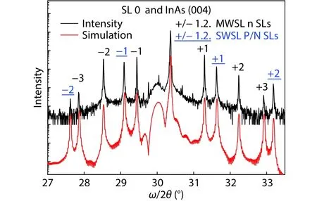
Fig.2.(Color online) HR-XRD of the PNn structure device and the corresponding simulation curve.
The dark current density (Jd) and the differential resistance-area product (RA) at different temperatures are given in Figs.3(a) and 3(b).At –0.1 V, the PNn structure photodetector exhibits aJdof 8.9 × 10⁻⁵A/cm2at 150 K, whereas, at 200 K,Jdis 0.012 A/cm2.The corresponding differential resistance-area products are 2832 and 48 Ω·cm2at 150 and 200 K,respectively.The electrical performance of this detector is comparable to those reported for the HOT MWIR SL detectors grown by MBE[10,16].Fig.4 presentsJdas a function of detector temperature (ranging from 78 to 200 K) at a bias voltage of –0.1 V.The activation energies (ΔE) were fitted usingJdiff~T3exp[–Ea/(KbT)][17].The activation energy of about 253 meV was deduced at temperaturesT> 135 K.This value is closed to the designed absorber bandgap, indicating that this HOT MWIR photodetector is dominated by the diffusion mechanism.However, asT< 100 K, activation energy is fitted to be as low as 19 meV, implying that tunneling or surface leakage current is a dominated mechanism in the PNn device.
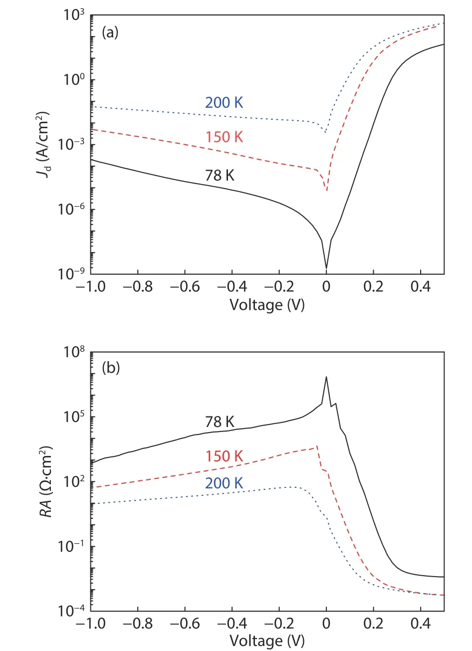
Fig.3.(Color online) (a) Jd versus voltage at different temperatures.(b) RA versus voltage at different temperatures.
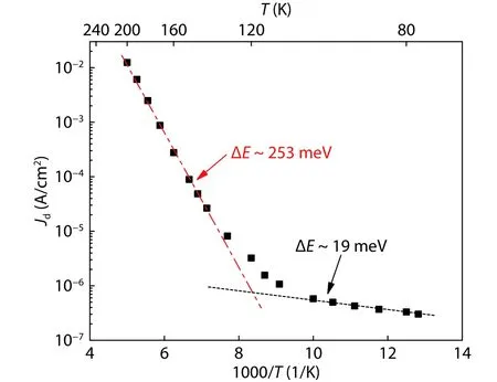
Fig.4.(Color online) Jd as a function of temperature at a bias voltage of –0.1 V.
Fig.5 shows spectral responsivity (Rλ) of the PNn device at different temperatures, which was measured by FTIR system (Nicolet IS50) with a 1000 K blackbody source.It can be seen that the cutoff wavelength keeps increasing as the temperature increase.Table 1 shows the 50% cutoff wavelengths at 78, 150, and 200 K.Under 78 K and –0.1 V, the peak responsivity (Rλ) of 0.26 A/W was measured at 4.1μm, corresponding to a quantum efficiency (QE) of 7.9%.The low QE is possibly due to the thinner absorption layer or/and a potential barrier between the N-SWSL layer and the n-MWSL layer.
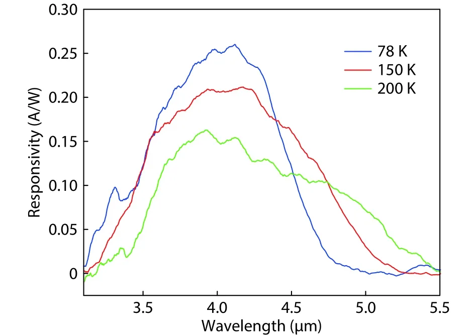
Fig.5.(Color online) Spectral responsivity (Rλ) of PNn device at different temperatures.

Table 1.50% cutoff wavelengths at 78, 150, and 200 K.
The specific detectivity (D*) at –0.1 V was estimated using the following equation:

whereRλis the responsivity,qis the electronic charge,kandTis Boltzmann’s constant and the temperature of the device,respectively.Fig.6 shows specific detectivity (D*) of the PNn device at different temperatures.At 78, 150, and 200 K, theD*was calculated to be 5.6 × 10¹¹, 3.2 × 10¹⁰, and 2.3 × 109cm·Hz1/2/W, respectively.TheD* decreases fast with temperature because of the exponentially increased dark current and reduced quantum efficiency.Although theD*of the PNn structure is less than those of the state-of-the-art HOT MWIR detectors grown by MBE[10,11], the PNn device structure grown by MOCVD shows potentials for HOT MWIR photodetectors.
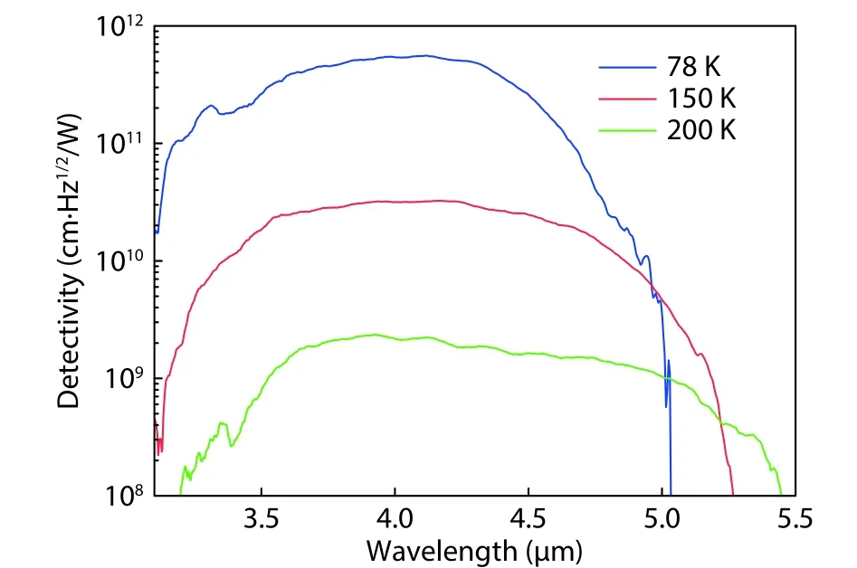
Fig.6.(Color online) Specific detectivity (D*) of the PNn device at different temperatures.
4.Conclusions
In summary, an aluminum-free heterojunction PNn-structure InAs/GaSb superlattice HOT MWIR photodetector grown by MOCVD has been demonstrated with an operating temperature up to 200 K.At 200 K and –0.1 V, the device exhibited aJdof 0.012 A/cm2and a peakD*of 2.3 × 109cm·Hz1/2/W.The quantum efficiency is low in this proof-of-concept device, but it can be improved using a thicker N-MWSL absorber combined with a lower doping level.These results suggest that the PNn design grown by MOCVD is a promising option for a HOT MWIR photodetector.
Acknowledgements
The authors are grateful for the ShanghaiTech University Quantum Device Lab.This project is supported partly by the Natural Science Foundation of China with Grant No.61874179, No.61804161, No.61975121 and No.61605236,and partly by the National Key Research and Development Program of China (No.2019YFB2203400).
杂志排行

Journal of Semiconductors的其它文章
- High-power InAlAs/InGaAs Schottky barrier photodiodes for analog microwave signal transmission
- Twist-angle two-dimensional superlattices and their application in (opto)electronics
- A 357.9 nm GaN/AlGaN multiple quantum well ultraviolet laser diode
- All-optical switching based on self-assembled halide perovskite microwires
- Alkali metal cation engineering in organic/inorganic hybrid perovskite solar cells
- F-containing cations improve the performance of perovskite solar cells