A 357.9 nm GaN/AlGaN multiple quantum well ultraviolet laser diode
2022-02-15JingYangDegangZhaoZongshunLiuFengLiangPingChenLihongDuanHaiWangandYongshengShi
Jing Yang, Degang Zhao,2,†, Zongshun Liu, Feng Liang, Ping Chen, Lihong Duan,Hai Wang, and Yongsheng Shi
1State Key Laboratory of Integrated Optoelectronics, Institute of Semiconductors, Chinese Academy of Sciences, Beijing 100083, China
2School of Electronic, Electrical and Communication Engineering, University of Chinese Academy of Sciences, Beijing 100049, China
Ultraviolet (UV) and deep-UV light emitters are promising for various applications including bioagent detection, water and air purification, dermatology, high-density optical storage, and lithography.However, to achieve shorter UV laser diodes (LDs), especially for the LDs with lasing wavelength less than 360 nm, requires high AlN mole fraction AlGaN cladding layer (CL) and waveguide (WG) layers, which usually leads to generate cracks in AlGaN epilayer due to lack of lattice-matched substrates.Meanwhile, due to high resistivity of high AlN mole fraction Mg doped AlGaN layers, only few groups have reported GaN-based LDs with emission wavelength shorter than 360 nm[1−8], and up to now, there is no room temperature continuous-wave (CW) operation UV LDs with a lasing wavelength shorter than 360 nm ever reported.Previously, we have reported a UV LD with lasing wavelength of 366 nm[9].In this paper, a higher AlN mole fraction of AlGaN WG layers is employed to shorten the LD emission wavelength to less than 360 nm.A lasing wavelength of 357.9 nm is achieved.
Firstly, two GaN-based UV LD structures with different AlN mole fraction of AlGaN WG layers were grown onc-plane GaN substrate by metal organic chemical vapor deposition(MOCVD), TMGa/TEGa, TMAl, TMIn and NH3were used as Ga,Al, In and N sources, respectively.The schematic diagram of the structure of GaN-based UV LDs is shown in Fig.1(a).It consists of a 1-μm thick n-type GaN layer, a 500 nm n-type Al0.07Ga0.93N cladding layer (CL) with n-doping concentration of 3 × 1018cm–3, a 20 nm n-type Al0.25Ga0.75N hole blocking layer (HBL), a AlGaN lower WG (LWG) layer, an unintentional doped GaN/Al0.07Ga0.93N multiple quantum well (MQW) active region, a AlGaN upper WG (UWG) layer, a 20-nm p-type Al0.3Ga0.7N electron blocking layer (EBL), a 500-nm p-type Al0.07Ga0.93N CL layer, and a 40 nm p-GaN contact layer.After the epitaxial growth, a 10μm-wide ridge stripe along the<1-100> direction was formed by dry etching on the epitaxial layers.The cavity of the laser diode with a length of 600μm was fabricated by cleaving the epitaxial film and substrate together along the {1-100} plane.A Ni/Au contact was evaporated onto the p-type GaN layer and a Ti/Al contact was evaporated onto the n-type GaN layer.Then the output power versus current (P–I) curves were recorded at room temperature using a calibrated Si detector.
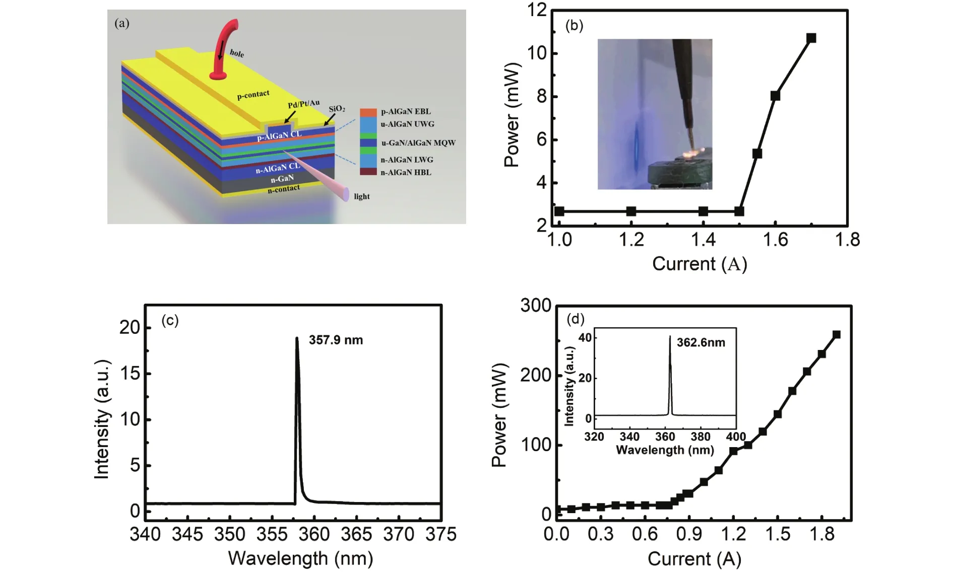
Fig.1.(a) Schematic diagram of LD structure.(b) Output power of LD1 as a function of injected direct-current measured at room temperature(RT).The inset shows a photo of the laser with the blue far field pattern of the laser beam formed on the white paper screen.(c) Electroluminescence spectrum of UV LD1 under RT pulsed operation condition at an injection current of 1550 mA.The pulse width was 50 ns and the repetition rate was 10 kHz.(d) P−I curve of UV LD2 under RT pulsed operation condition, the inset shows it has a lasing wavelength of 362.6 nm at an injection current of 800 mA.
The RT output power of one fabricated UV LDs, LD1,which is with about 4.5% AlN mole fraction AlGaN WG layers,as a function of injected current is measured under pulsed operation condition and shown in Fig.1(b).It is found that the output power of LD1 is nonlinear with the injection current and it has an abrupt increase at the injection current of 1.5 A, corresponding to 25 kA/cm2.This threshold current value of lasing is similar to the reported ones by other groups[3,4,10–12].The output power is about 11 mW at an injection current of 1.7 A.The inset shows the photo of lasing LD1 and the far field pattern of laser beam in blue color formed on the white paper screen.The leakage modes in the laser beam are not observed because the UV light should be absorbed by thick GaN layers existing in both n side and p side.
Fig.1(c) shows the electroluminescence spectrum of UV LD under pulsed operation condition at an injection around the threshold current of 1550 mA.It can be seen that the peak wavelength is 357.9 nm, and the full width at half maximum (FWHM) is about 0.3 nm which is obtained by Gaussian fitting to the emission peak.
Another prepared UV LD, LD2, has a lower AlN mole fraction of AlGaN WG layer, which is approximately 3.5% for both lower and upper WG layers.The front and rear cleaved facets of laser diode were uncoated.TheP–Icurve and stimulation emission spectrum of LD2 are presented in Fig.1(d).Compared with LD1, the wavelength of stimulation emission increases about 5 to 362.6 nm.Such an increase is attributed to the increased absorption of high energy UV light in the Al-GaN WG layers with lower AlN mole fraction.In addition, it is found that in comparison with LD1, the optical characteristics of LD2 are improved obviously.The threshold current of LD2 is 760 mA, corresponding to 12.7 kA/cm2.The output power is 258 mW at the injection current of 1.9 A and the slope efficiency is about 0.23 W/A.
The higher threshold current density of LD1 compared with LD2 may be attributed to the weaker optical confinement factor, which is due to a smaller difference in the AlN mole fraction of AlGaN CL and WG layers for LD1.It leads to a large percentage of light penetrating into CL or even to GaN layers.Therefore, the absorption loss of LD1 is larger than that of LD2.However, it is noted that during the growth of Al-GaN WG layers with higher Al composition, the stress at hetero-structure will increase, additional attention should be taken to ensure the structural quality of laser diodes.Such a comparative analysis means that it is difficult to achieve high performance UV LD with a shorter stimulation wavelength,and some methods must be introduced to obtain higher AlN mole fraction AlGaN CL and WG layers but without increasing stress.
In summary, UV LD with a short emission wavelength at 357.9 nm has been fabricated successfully with a 10 ×600μm2ridge wave guide structure.When the LD is operated in pulsed condition, the threshold current is about 25 kA/cm2and the peak output power is 11 mW.The characteristics are improved obviously when the lasing wavelength increases to 362.6 nm.A comparative analysis indicates that it is a huge challenge to further decrease the lasing wavelength of UV LDs.
Acknowledgements
This work was supported by the National Natural Science Foundation of China (Grant Nos.62034008, 62074142,62074140, 61974162, 61904172, 61874175), the Youth Innovation Promotion Association of Chinese Academy of Sciences(Grant No.2019115), Beijing Nova Program (Grant No.202093), Beijing Municipal Science and Technology Project(Grant No.Z211100007921022) and the Strategic Priority Research Program of Chinese Academy of Sciences (Grant No.XDB43030101).
杂志排行
Journal of Semiconductors的其它文章
- High-power InAlAs/InGaAs Schottky barrier photodiodes for analog microwave signal transmission
- Twist-angle two-dimensional superlattices and their application in (opto)electronics
- All-optical switching based on self-assembled halide perovskite microwires
- Alkali metal cation engineering in organic/inorganic hybrid perovskite solar cells
- F-containing cations improve the performance of perovskite solar cells
- Anisotropic 2D materials for post-Moore photoelectric devices