Alkali metal cation engineering in organic/inorganic hybrid perovskite solar cells
2022-02-15JilinWangRuibinTangLixiuZhangFeiLongDishengYaoandLimingDing
Jilin Wang, Ruibin Tang, Lixiu Zhang, Fei Long, Disheng Yao,†, and Liming Ding,†
1School of Materials Science and Engineering, Key Laboratory of New Processing Technology for Nonferrous Metals and Materials (MoE),Guilin University of Technology, Guilin 541004, China
2Guangxi Key Laboratory of Optical and Electronic Materials and Devices, Guilin University of Technology, Guilin 541004, China
3Center for Excellence in Nanoscience (CAS), Key Laboratory of Nanosystem and Hierarchical Fabrication (CAS), National Center for Nanoscience and Technology, Beijing 100190, China
The past decade has witnessed the rapid advance in organic–inorganic hybrid perovskite solar cells (PSCs).Owing to unique optoelectronic properties of perovskites, the power conversion efficiency (PCE) of PSCs has jumped from 3.8% to 25.5%[1–4].However, under the stimulus of illumination, moisture, oxygen and heat, perovskites exhibit unsatisfactory stability due to weak bonding among the components in these soft-lattice crystals[5–7].Doping and passivation engineering with alkali metal cations can enhance the intrinsic stability of perovskite materials.Here, the recent progress of alkali metal cations engineering is reviewed, and the impact on the crystallization, lattice structure, photovoltaic performance and stability is discussed.
The doping of alkali metal cations has been explored recently[8,9].Cs+and Rb+can occupy A-site in perovskite lattice(Fig.1(a)).The smaller Cs+(1.69 Å) in MA/FA perovskites reduces the tolerance factor, shifting crystal structure towards a cubic form to stabilize photoactiveα-FAPbI3phase.Fig.1(b)shows XRD patterns of MA/FA perovskites with different Cs+content[10].The sample without Cs+(black curve) showed small peaks at 11.61° and 12.71°, corresponding to photo-inactive δ-FAPbI3and PbI2, respectively.When doping Cs+, these peaks vanished, indicating that Cs+in perovskites could inhibit the formation of yellow phase.In addition, Cs+can enhance the thermal and humidity stability of perovskite materials and devices[11−13].The effect of Cs+content on thermal stability is shown in Fig.1(c).This work indicated that perovskite degradation was associated with oxygen in air.Cs+doping (molar ratiox= 0.09) can hinder the interaction between perovskite and oxygen.
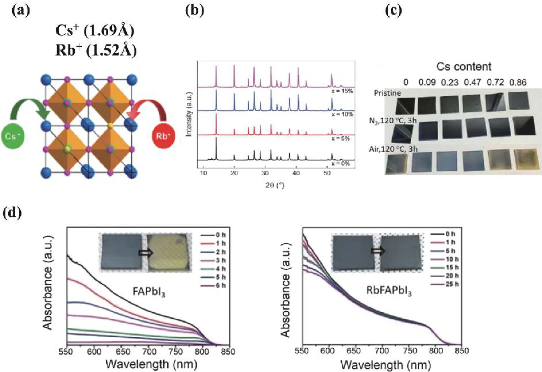
Fig.1.(Color online) (a) Illustration of Cs+ and Rb+ positions in perovskite lattice.(b) XRD patterns for CsxMAFA perovskites (x = 0%, 5%, 10%,15%).Reproduced with permission[10], Copyright 2016, Royal Society of Chemistry.(c) Perovskite films with different Cs+ content exposed to different atmosphere.Reproduced with permission[11], Copyright 2017, Royal Society of Chemistry.(d) Absorbance change of FAPbI3 (Left) and Rb0.05FA0.95PbI3 (Right) perovskite films stored in the dark at 85% RH for different durations.Reproduced with permission[14], Copyright 2017,John Wiley & Sons.
Parket al.[14]reported that Rb+could improve the humidity stability of RbxFA1–xPbI3solar cells.The absorption spectra of RbxFA1–xPbI3film barely changed in ambient environment(Fig.1(d)).While the absorbance of FAPbI3film decreased significantly and began to decompose within 6 h.Gratzelet al.[15]introduced Rb+into perovskite to form a quadruple-cation compound named RbCsMAFA.The PbI2and δ-FAPbI3peaks were weakened, implying that Rb+could be incorporated into the lattice and adjust crystal structure like Cs+.Encapsulated solar cells with Rb+kept 95% of their initial performance after 500 h at 85 °C.Rb+incorporation can effectively alleviate defect migration in mixed halide perovskite[16].Rb+doping yields high-performance PSCs with negligible hysteresis and enhanced stability.
K+could effectively passivate defects at both grain boundaries (GBs) and interfaces, inhibiting halide anions migration under light illumination[17,18].Owing to the small ionic radius(1.38 Å) of K+, some studies indicated that it could not occupy the A-site of perovskite lattice but enter the interstitial position (Fig.2(a))[19].K+inhibits the formation of I-Frankel defects which is regarded as the origin of the current–voltage(J–V) hysteresis (Fig.2(b)).Based on density functional theory(DFT) calculation, Zhaoet al.demonstrated that K+prefers interstitial occupation to A-site occupation, which increases the ion-migration energy barrier and inhibits photoinduced phase separation[20].
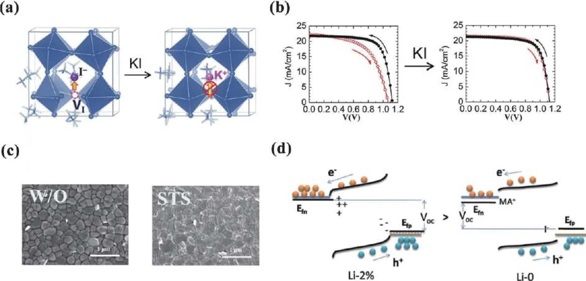
Fig.2.(Color online) (a) K+ occupies the interstitial sites and inhibits the formation of I-Frankel defects.(b) J−V curves for perovskite solar cells without and with KI doping under forward and reverse scans.Reproduced with permission[19], Copyright 2018, American Chemical Society.(c)SEM images for films without/with STS.Reproduced with permission[23], Copyright 2020, John Wiley & Sons.(d) The enlarged quasi-Fermi level splitting.Reproduced with permission[25], Copyright 2017, John Wiley & Sons.
Though Na+and Li+are too small to occupy the A-site in lattice, they can affect device performanceviaadjusting crystallization process and passivating defects at GBs and interfaces.Doping Na+into the precursor solution could improve the crystal quality of perovskite films[21,22].In addition, surface passivation with Na+is a feasible approach to reduce defects.Fig.2(c) shows surface topographic scanning electronic microscopy (SEM) images without/with sodium p-toluenesulfonate (STS) between perovskite layer and hole-transport layer[23].Though there is negligible change for overall surface morphology of perovskite film, the formation of tiny bright particles (~25 nm) around the grains was clearly observed in the sample with STS, which could passivate non-radiative recombination centers at GBs.Na+could interact with the under-coordinated halide anions (I/Br) at perovskite surface, reducing surface trap states and improving device performance.Li+could occupy interstitial positions[24].Zhanget al.[25]introduced a small amount of LiI into the frame of perovskite crystals.Certain ion migration and aggregation in perovskite led to N/P doping.The cations (e.g.MA+, Li+) accumulated at perovskite/PCBM interface and anions (e.g.I−) at perovskite/NiOxinterface (Fig.2(d)).As a result, an ionic built-in field formed with a direction from N to P, assisting carriers transport and extraction.Besides, the accumulated ions lifted quasi-Fermi level of n side (Efn) while lowered that of p side (Efp), thus increasingVoc.
In short, alkali metal cation engineering is a positive approach.The exact location of alkali metal cations in perovskite films is still ambiguous.More experimental and theoretical investigation is required.
Acknowledgements
F.Long thanks the National Natural Science Foundation of China (51972071), Guangxi Distinguished Experts Special Fund (2019B06), Guangxi Research Foundation for Science and Technology (AD19245175), and Guangxi Key Laboratory of Optical and Electronic Materials and Devices (20AA-19).D.Yao thanks Guilin University of Technology research fund(GUTRD2000002727).L.Ding thanks the National Key Research and Development Program of China(2017YFA0206600) and the National Natural Science Foundation of China (51773045, 21772030, 51922032, 21961160720)for financial support.
杂志排行

Journal of Semiconductors的其它文章
- High-power InAlAs/InGaAs Schottky barrier photodiodes for analog microwave signal transmission
- Twist-angle two-dimensional superlattices and their application in (opto)electronics
- A 357.9 nm GaN/AlGaN multiple quantum well ultraviolet laser diode
- All-optical switching based on self-assembled halide perovskite microwires
- F-containing cations improve the performance of perovskite solar cells
- Anisotropic 2D materials for post-Moore photoelectric devices