High-power InAlAs/InGaAs Schottky barrier photodiodes for analog microwave signal transmission
2022-02-15ZhuravlevChizhMikitchukGilinskyChistokhinValishevaDmitrievToropovandAksenov
K.S.Zhuravlev, A.L.Chizh, K.B.Mikitchuk, A.M.Gilinsky, I.B.Chistokhin, N.A.Valisheva,D.V.Dmitriev, A.I.Toropov, and M.S.Aksenov
1A.V.Rzhanov Institute of Semiconductor Physics, The Siberian Branch of the Russian Academy of Sciences, Ac.Lavrentiev Avenue 13,Novosibirsk 630090, Russia
2Laboratory of Microwave Photonics, SSPA “Optics, Optoelectronics and Laser Technology” of National Academy of Sciences of Belarus,Logoiski trakt 22, Minsk 220090, Belarus
Abstract: The design, manufacturing and DC and microwave characterization of high-power Schottky barrier InAlAs/InGaAs back-illuminated mesa structure photodiodes are presented.The photodiodes with 10 and 15 μm mesa diameters operate at≥40 and 28 GHz, respectively, have the output RF power as high as 58 mW at a frequency of 20 GHz, the DC responsivity of up to 1.08 A/W depending on the absorbing layer thickness, and a photodiode dark current as low as 0.04 nA.We show that these photodiodes provide an advantage in the amplitude-to-phase conversion factor which makes them suitable for use in highspeed analog transmission lines with stringent requirements for phase noise.
Key words: InAlAs/InGaAs heterostructures; microwave photodiodes; microwave photonics
1.Introduction
The advancement of high-power photodiodes operating in the gigahertz frequency range has enabled the creation of fiber-based systems of long-haul transmission of analog microwave signals that provide the advantages of low signal loss, immunity to electromagnetic interference and light weight[1–5].Various designs of high-power photodiodes have been considered so far.Achieving optimal photodiode parameters requires optimization of various design key points, including charge carrier transit time, structure capacitance and conductivity, and heat removal, which frequently implies a compromise in parameters.Most of the designs of the highpower photodiodes described so far were based upon the p–i–n semiconductor structures.A Schottky barrier photodiode design employing a back-illumination scheme provides several advantages over the p–i–n-based structures, which include a lower electrical resistance of the photodiode leads and a larger thermal conductivity of two massive bulk leads as well as the possibility to use the optical reflection of the non-alloyed Schottky metal contact to increase the total absorption efficiency in the absorbing layer of the structure[6].We have recently demonstrated the Schottky barrier photodiodes in high-power operation[7].In this paper we describe the design, manufacturing and characterization of highpower Schottky barrier back-illuminated mesa structure photodiodes based on InAlAs/InGaAs heterostructures, and discuss the advantages of this type of microwave photodiodes for the 1.2–1.6μm wavelength range.The operation of 10 and 15μm diameter photodiodes in the frequency ranges of ≥40 and 28 GHz, respectively, the output power of up to 58 mW at 20 GHz, the responsivity of up to 1.08 A/W, and a photodiode dark current as low as 0.04 and 0.1 nA for 10 and 15μm diameter diodes, respectively, were achieved.A study of the amplitude-to-phase (AM-PM) noise conversion characteristics of the manufactured photodiodes showed that the Schottky barrier photodiodes provide an advantage in the amplitudeto-phase conversion factor.This makes the Schottky barrier photodiodes a promising candidate for use in high-speed analog transmission lines with stringent requirements for the phase noise such as optoelectronic oscillators, analog optic transmission links and distributed antenna arrays.
2.Photodiode fabrication
The heterostructures for photodiode manufacturing were produced by molecular beam epitaxy using a Riber Compact 21T system.The growth was performed on substrates of semi-insulating InP (001) which provided low free-carrier light absorption for the back-illuminated photodiode design.One of the most important stages in the growth sequence was the substrate cleaning procedure prior to the layer growth.In order to initiate the growth on an atomically clean surface,the substrate was annealed at temperatures up to 540 °C in an arsenic flux with an equivalent beam pressure of 2.5 ×10⁻⁵Torr.The preparation of the substrate surface was monitored using a reflection high-energy electron diffraction(RHEED) system.The anneal was carried out until the appearance of surface reconstructions indicating that a clean surface has been reached.Fig.1 displays RHEED images showing the creation of the (4 × 2) surface reconstruction which indicates the complete removal of residual oxides and the forma-tion of a clean substrate surface suitable for the heterostructure growth.The details of surface transformations during the substrate preparation were discussed in Ref.[8].

Fig.1.(Color online) The (4 × 2) reconstruction of the clean surface of(001) InP after annealing seen in the RHEED images: (a) the[10]azimuth, (b) the [110] azimuth.The arrows indicate reflexes corresponding to the period by (a) 4 times and (b) 2 times greater than the crystal lattice period.
The heterostructures used for the photodiode fabrication utilized a phosphorus-free InAlAs/InGaAs layer design which reduced the complexity of the growth procedure and system support in comparison with P-containing structures.The design of the heterostructure is given in Table 1 and the photodiode energy band diagram is shown schematically in Fig.2.The structure consisted of a light absorbing layer which in turn comprised two parts, namely an undoped part and a thin n+-doped part, an n-side strongly doped contact layer below it, and a layer sequence used for the formation of the Schottky barrier grown above the absorbing layer.The thin n+-InGaAs absorbing layer and the graded bandgap In-GaAlAs layer helped to eliminate the accumulation of charge carriers at the InAlAs/InGaAs heterointerfaces, which could lead to a significant increase of the carrier transfer time and,therefore, to a limitation of the photodiode bandwidth.The top protective InGaAs layer prevented the InAlAs surface from oxidation before the fabrication of the Schottky barrier.The InAlAs and InGaAs layers were grown at temperatures of 520 and 480 °C, respectively.ThexInAscontents in the layers were calibrated using the photoluminescence and optical absorption techniques prior to the growth of each heterostructure.The quality of the grown single layers and heterostructures was evaluated using the X-ray diffraction[9], atomic force microscopy (AFM), and scanning electron microscopy(SEM).A deviation of thexInAsfrom the lattice-matched values ofxInAs= 0.53 for InxGa1–xAs andxInAs= 0.52 for InxAl1–xAs alloys of not more than 0.2% was generally accepted throughout this study.The peak-to-peak roughness of the surface of the multilayer heterostructures, as observed by the AFM, did not exceed 0.8 nm which corresponded closely to the r.m.s.value of 0.113 nm that was obtained on single-layer samples previously[9].A SEM picture of a cleaved as-grown heterostructure shows distinct layer boundaries (Fig.3) which confirms the achievement of the coherent two-dimensional growth mode required for the synthesis of high-quality heterostructures.
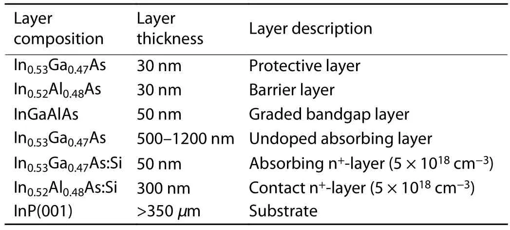
Table 1.InAlAs/InGaAs heteroepitaxial structure of the Schottky barrier high-power microwave photodiode.
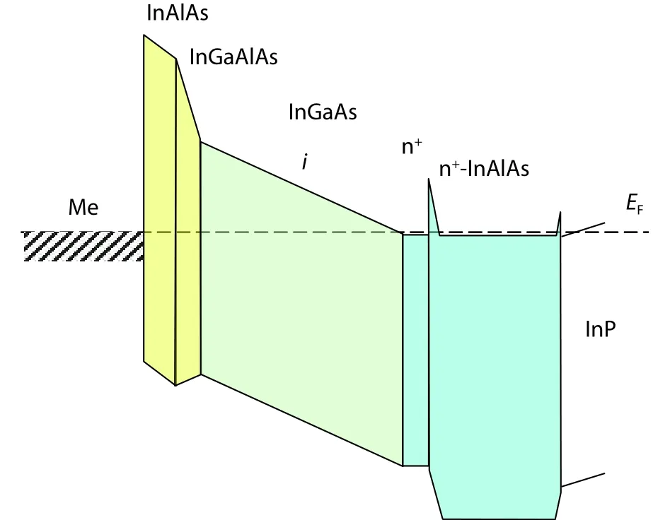
Fig.2.(Color online) Energy band diagram of the InAlAs/InGaAs Schottky barrier photodiode under zero bias voltage.EF is the Fermi level and Me is the Schottky barrier metal.

Fig.3.(Color online) A SEM picture of a heterostructure sample with a total intended thickness of the absorbing layer of 650 nm.Layers of In-GaAs appear brighter in intensity than InAlAs-based layers.The visible sets of different contrast layers are, from top to bottom: the In-AlAs barrier and InGaAlAs graded bandgap layers together with the In-GaAs protective layer; the InGaAs absorbing layer; the n+-InAlAs contact layer; the InP substrate.The green marks denote the layer thicknesses as seen by the SEM.
The photodiodes were fabricated by forming mesa structures by a two-step chemical etching of the heterostructures in an H3PO4: H2O2: H2O = 1 : 1 : 38 solution.The mesas with diameters ranging from 10 to 40μm were manufactured.The ohmic contact to the n+-InAlAs layer was fabricated by depositing layers of Ge/Au/Ni/Au (20/40/20/200 nm) followed by an annealing at 385 °C in a hydrogen atmosphere.The Schottky barrier was formed by the deposition of Ti/Au (20/200 nm)on the InAlAs surface of the mesa structure.The use of a large bandgap InAlAs layer allowed one to increase the barrier height as compared to metal-InGaAs Schottky barrier structures.Prior to the barrier formation the InGaAs protective layer and native oxide of InGaAs protective layer were removed in succinic acid : peroxide = 5 : 1 and HCl : H2O = 1 : 10 solutions, respectively.The mesa surface was passivated with an 800 nm SiO2layer synthesized by the low-pressure chemical vapor deposition technique at 250 °C.Contact leads of 4.5–5μm thickness were formed by the electrochemical deposition of gold.The thick leads provided both a low electrical resistance and a high thermal conductivity to facilitate the heat removal from the diode.The mechanical strength of the structure was maintained by a polymer film.The substrate was thinned by mechanical grinding and chemical-mechanical polishing, after which an anti-reflection coating layer was deposited to minimize the light reflection.The wafer was then separated into individual back-illuminated diode chips.A photodiode chip is illustrated in Fig.4.
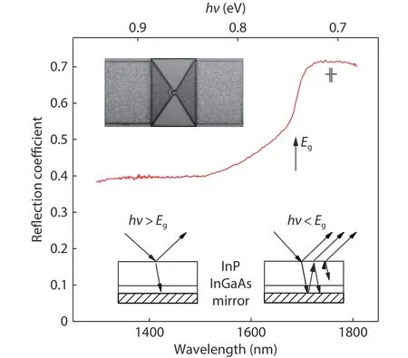
Fig.4.(Color online) Optical reflection spectrum of a model heterostructure used to evaluate the Schottky contact reflection efficiency.The spectral resolution is set to average the interference fringes that develop in the spectral region hν < Eg.The diagrams illustrate the mechanisms of reflection for photon energies hν above the bandgap Eg of the InGaAs absorbing layer (left) and for hν < Eg (right).The inset at the top shows the photograph of a photodiode chip.
3.Photodiode characterization
The DC parameters of the photodiodes were evaluated using an Agilent B1500A semiconductor device parameter analyzer, a Cascade M150 probe station, and a single mode fiber-coupled 1.55μm laser used for responsivity measurements under continuous-wave illumination.A double diffraction grating spectrometer was employed to study the optical reflection spectra of Schottky barriers.Microwave characterization was performed using an experimental setup build around a distributed feedback laser diode with an erbium doped fiber amplifier, a 40-GHz bandwidth Mach-Zender electrooptic light intensity modulator, an Anritsu MS4645B vector network analyzer and an Anritsu MA24126A power meter.The photodiode chips were flip-chip mounted to carrier boards with 50 Ω grounded coplanar waveguide lines and end-launch K connectors.
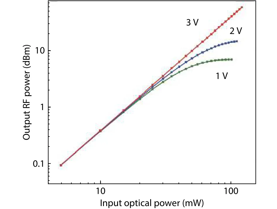
The DC current–voltage dependencies of the diodes were typical of Au/Ti-InAlAs Schottky diodes and displayed a barrier height of 0.7 eV and an ideality factor of 1.2[10].The average values of the dark current taken at a 3 V bias on bunches of photodiodes of 20 pcs each amounted to 0.04, 0.1 and 0.3 nA for diode diameters of 10, 15 and 40μm, respectively.The responsivity of the photodiodes depends on the absorbing layer thickness and is also influenced by the amount of incident light that had passed through the absorbing layer and is reflected backwards by the Schottky contact that acts as a mirror.In order to assess the amount of the contact reflection, we evaluated the reflection coefficientRSof the Schottky contact.TheRSwas determined from the spectrum of the reflection coefficientR(λ) of a specially prepared large-square sample that was not separated into diode mesas.The substrate of this sample was not thinned and had no antireflection coating.This resulted in the development of interference fringes in the spectral range below the InGaAs absorbing layer bandgapEg= 0.74 eV due to the light reflections between the semiconductor–air interface and the Schottky metal mirror.The interference period in the spectrum was approximately equal to 1 nm.TheR(λ) spectrum taken at 45°angle of incidence is shown in Fig.4.The spectral resolution of the spectrometer was set so as to average the interference fringes during this measurement.The spectrum comprises two parts.At photon energieshνabove the absorbing layer bandgap the reflection coefficient is determined mostly by the reflection at the substrate–air interface.In this case,the reflection is dominated by the component of light polarized perpendicularly to the plane of incidence andR(λ)reaches 38% forhνabove 0.85 eV.At photon energieshν The dependence of the photodiode responsivity at a 1.55μm wavelength on the absorbing layer thickness is shown in Fig.5.The photodiodes were illuminated from the substrate side using a cleaved fiber positioned opposite to the mesas.The measurement was performed on photodiodes with the largest mesa diameters in order to minimize the loss of light.The responsivity reached 1.08 A/W for an absorbing layer thickness of 1200 nm.The theoretical model values for the responsivity calculated according to Ref.[12]with the reflection of the Schottky barrier taken into account and assuming an absorption coefficient ofα= 7050 cm–1(see Ref.[13]) and a negligible reflection at the coated chip surface (the solid curve) approximate the experimental data well. Fig.5.(Color online) The dependence of the photodiode responsivity on the absorbing layer thickness at a wavelength of 1.55 μm.Squares display the experimental data and the solid line is a model calculation. Although a larger thickness of the absorbing layer results in a larger responsivity of a photodiode, it also leads to an increase in the charge carrier transit time and therefore limits the photodiode bandwidth[14].For this reason the measurements of the photodiode frequency response were performed on photodiodes with the smaller thickness of the absorbing layer.Fig.6 depicts the frequency responses of photodiodes with mesa diameters of 10 and 15μm that have low capacitances and display the largest bandwidths.Here, the drops on the low-frequency side of the response curves are caused by the frequency responses of the high-pass bias circuits on the chip carrier boards.The ‘wavy’ behavior of the curves is induced by two unfavorable side effects: the incomplete matching of the impedances of the photodiode and transmission line, and non-ideality of the light intensity modulator calibration.It is seen from the figure that the frequency range of the 15μm diameter photodiodes is limited to 28–30 GHz while that of the 10μm photodiodes extends over 40 GHz.The limitation of the frequency range of the 15μm photodiodes is attributed to the largerRCtime constant value of the circuit (hereR= 50 Ω being the load impedance)due to the larger diode capacitance.The largest output microwave power was achieved from photodiodes with the 15μm diameter.Fig.7 shows the dependencies of the microwave power output of a 15μm photodiode on the input modulated optical power taken at a modulation frequency of 20 GHz for various applied bias voltages.The maximum output power, which caused thermal failure of the devices,reached as much as 58 mW at a bias voltage of 3 V.The output power value attained compares well with the data on the partially depleted absorber (PDA) and uni-traveling-carrier(UTC) photodiodes of comparable sizes in this frequency range (see e.g.Refs.[2, 15]). Fig.6.(Color online) The frequency response of a 10 μm (solid line)and 15 μm (dashed line) diameter photodiodes. Fig.7.(Color online) RF output power of a 15 μm diameter photodiode as a function of the input optical power for bias voltages of 1, 2 and 3 V.Modulation frequency 20 GHz. Another important characteristic of a high-power photodiode that can limit its application to microwave measurement and communication systems, phased antenna arrays and optoelectronic oscillators is the phase noise induced by the photodiode due to a variation of the output signal phase with a change in the input laser intensity.As a result of the dependence of the output signal phase on the input power level due to nonlinearities of the photodiode, the laser intensity noise is converted to an additional phase noise at its output[16–18].The amplitude to phase noise conversion can be characterized by the conversion coefficientKPD= ΔφPD/ ΔPopt[rad/W],where ΔPoptis the input light power change and ΔφPDis the output phase change.To evaluate theKPDof the manufactured Schottky photodiodes, a dependence of the output signal phase versus the incident light power was measured at a modulation frequency of 20 GHz.The light power was recorded by taking the DC photocurrent of the photodiode.Fig.8(a) depicts the fits to the phase change dependencies of a 15μm diameter photodiode RF output measured for bias voltages from 1 to 3 V.It is seen from the figure that the output phase demonstrates a nonmonotonic behavior: an initial rise with the light power increased is followed by a decrease.The calculated absolute values of theKPDcoefficient obtained by the fitting of data of Fig.8(a) are shown in Fig.8(b).TheKPDobtained for the 3 V bias voltage which corresponded to the largest output power of the photodiode does not exceed 1.5 rad/W and exhibits a null at a photodiode DC current of 24 mA.The value ofKPDachieved can be compared with the published parameters of commercial photodiodes.According to Ref.[19], theKPDof xHPLD series high-power photodiodes by Discovery Semiconductor, Inc.is limited to 5 rad/W.This comparison shows the advantage of the Schottky photodiode design, which makes these photodiodes suitable for use in high-speed analog fiber-optic transmission links with stringent requirements for phase noise. Fig.8.(Color online) (a) Dependence of the phase of the output RF signal of a 15 μm diameter photodiode on the photodiode photocurrent for bias voltages of 1, 2 and 3 V.(b) Amplitude-to- phase conversion coefficient dependencies calculated from the data of (a). We described the design, manufacturing and characterization of high-power Schottky barrier InAlAs/InGaAs back-illuminated mesa structure photodiodes.These photodiodes of a 10 and 15μm diameter operate in the frequency ranges of≥40 and 28 GHz, respectively, and demonstrate the output RF power as high as 58 mW at a frequency of 20 GHz, the DC responsivity of up to 1.08 A/W, and a photodiode dark current as low as 0.04 nA.An AM-PM conversion coefficient of 1.5 rad/W has been measured, which makes the Schottky barrier photodiodes suitable for use in high-speed analog fiberoptic transmission links and optoelectronic oscillators with stringent requirements for phase noise. Acknowledgements The preparation and processing of heterostructures used in this work was supported by the Russian Science Foundation (grant number 19-72-30023).


4.Conclusion
杂志排行
Journal of Semiconductors的其它文章
- Twist-angle two-dimensional superlattices and their application in (opto)electronics
- A 357.9 nm GaN/AlGaN multiple quantum well ultraviolet laser diode
- All-optical switching based on self-assembled halide perovskite microwires
- Alkali metal cation engineering in organic/inorganic hybrid perovskite solar cells
- F-containing cations improve the performance of perovskite solar cells
- Anisotropic 2D materials for post-Moore photoelectric devices
