Twist-angle two-dimensional superlattices and their application in (opto)electronics
2022-02-15KaiyaoXinXingangWangKasperGroveRasmussenandZhongmingWei
Kaiyao Xin, Xingang Wang, Kasper Grove-Rasmussen, and Zhongming Wei,†
1State Key Laboratory of Superlattices and Microstructures, Institute of Semiconductors, Chinese Academy of Sciences, Beijing 100083, China
2Center for Quantum Devices & Nano-Science Center, Niels Bohr Institute, University of Copenhagen, Copenhagen Ø 2100, Denmark
3Sino-Danish Center for Education and Research, Sino-Danish College, University of Chinese Academy of Sciences, Beijing 100049, China
Abstract: Twist-angle two-dimensional systems, such as twisted bilayer graphene, twisted bilayer transition metal dichalcogenides, twisted bilayer phosphorene and their multilayer van der Waals heterostructures, exhibit novel and tunable properties due to the formation of Moiré superlattice and modulated Moiré bands.The review presents a brief venation on the development of “twistronics” and subsequent applications based on band engineering by twisting.Theoretical predictions followed by experimental realization of magic-angle bilayer graphene ignited the flame of investigation on the new freedom degree, twistangle, to adjust (opto)electrical behaviors.Then, the merging of Dirac cones and the presence of flat bands gave rise to enhanced light-matter interaction and gate-dependent electrical phases, respectively, leading to applications in photodetectors and superconductor electronic devices.At the same time, the increasing amount of theoretical simulation on extended twisted 2D materials like TMDs and BPs called for further experimental verification.Finally, recently discovered properties in twisted bilayer h-BN evidenced h-BN could be an ideal candidate for dielectric and ferroelectric devices.Hence, both the predictions and confirmed properties imply twist-angle two-dimensional superlattice is a group of promising candidates for next-generation (opto)electronics.
Key words: twist angle; Moiré superlattice; two-dimensional; (opto)electronics
1.Introduction
From the successful fabrication of atomically thin carbon films by Andre Geim and Konstantin Novoselov through mechanical exfoliation in 2004[1], graphene not only verified the possibility for stable existence of two-dimensional materials but also exhibited novel and outstanding physical properties including ultra-high carrier mobility[2], ultra-high thermal conductivity[3]and superior mechanical properties[4], which was awarded the Nobel prize in physics 2010.Subsequently, investigations on exploring new 2D materials and their applications have become the frontier fields in condensed physics, such as graphyne[5,6], two-dimensional transition metal dichalcogenides (TMDs)[7−12], MXenes[13], hexagonal boron nitride (h-BN)[14,15], black phosphorene (BP)[16,17], black arsenic[18,19].By breaking the weak van der Waals interaction between layers as a “top-down” method like exfoliation or aggregating atoms together as a “bottom-up” method like chemical vapor deposition, researchers have developed variable methods to produce versatile two-dimensional materials and fabricated diverse devices like a field-effect transistor, photodetector and PN diode based on their suitable electronic structures and atomic size along the out-of-plane direction[20−23].
Undoubtably, as the first discovered and the most popular 2D material, graphene has attracted the most attention on its physical properties and the exploration for more potential applications.For instance, recently, graphene was even used as a holder for transmission electron microscopy[24]or just vertically stacked to serve as a kind of thermal interface material[25].Now it is generally accepted that after getting rid of interlayer interaction, electrons in graphene around the Fermi level will follow linear energy dispersion, which is supposed to be described by Dirac equation, indicating zero static mass theoretically[26,27].However, the semi-metal behavior induced by the lack of bandgap significantly confined the application of graphene in electronics[28].Therefore, versatile accesses, which contain doping, oxidization[29,30], stacking with other 2D materials to form van der Waals heterojunctions[31,32]or twisting bilayer graphene[33], were focused on band engineering in order to obtain new electrical properties.Among them, twisting has irreplaceable merits, providing an impurity-free single-material platform and the presence of a new freedom degree to the system, twistangle[34−36](Fig.1(a) and 1(b)).

Fig.1.(Color online) Merging of two Dirac cones and the presence of flat bands.(a) Twisted Brillouin zones from upper and lower graphene sheets (colored by red black and red) with θ.(b) Schematic of merging of the two Dirac cones between Ka and Kb points (left) in (a) and the corresponding distribution of density of states (right).Reproduced with permission[36].Copyright 2012, American Physical Society.(c) Theoretical simulation on the band structure of TBLG at 1.6°, 1.3° and 1.0° by tight-binding calculations, leading to the presence of flat bands at twist-angle of 1.6°and 1.3°.Reproduced with permission[38].Copyright 2010, American Physical Society.(d) Electric-field tunable VHSs in two merging Dirac cones observed by nanoARPES.Reproduced with permission[41].Copyright 2020, WILEY-VCH Verlag GmbH & Co.KGaA, Weinheim.(e) Flat bands in TBLG near the magic-angle and their local density of states through mean-field theory.Reproduced with permission[45].Copyright 2018, American Physical Society.
In 2007, Lopes dos Santoset al.[37]assumed mismatched bilayer graphene sheets may bring novel electrical properties,even being transformed into superconductor in some cases.Thereout, theoretical simulations on twisted bilayer graphene(TBG) were ignited around the world.Three years later,Suarez Morellet al.[38]utilized tight-binding calculation to simulate electron behavior in slightly TBG and found that the energy band around Fermi level would be flattened when the twist-angle was around 1.5° (Fig.1(c)), giving rise to “infinite”effective mass and localized states which could be related with a correlated electron system.Such a flat band structure was not directly observed until 2020 by Lisietal.[39]in a TBG with a twist-angle of 1.34° through angle-resolved photoemission with simultaneous real- and momentum-space resolution (nano-ARPES).In 2011, Bistritzer and MacDonald[40]predicted the evolution of electronic structure with twist angle and the unique flat band structure at the precise twist angle of 1.05° in TBG.Besides, they found that the merging of two Dirac cones at 5° would generate van Hove singularities(VHSs) in density of states (DOS) which was confirmed by Joneset al.[41]in 2020 through nano-APERS (Fig.1(d)), leaving an opportunity for bandgap engineering in TBG.In 2017,Carret al.[42]extended the concept “twist-angle” to other 2D material systems and introduced “twistronics” to generalize the investigations on twisted 2D systems.It seemed theoretical simulations had made full preparation for experimental realization, but actually two high-quality graphene always tend to form AA or AB stacking mode spontaneously when they are just slightly twisted relatively.Therefore, in 2018, when Cao Yuan and Pablo Jarillo-Herrero demonstrated successful fabrication of 1.1° TBG by modified “tear and stack” technique and observed both Mott-like correlated insulator behavior[43]and unconventional superconductivity[44], it provided convincing evidence for the correctness of former theoretical predictions, hence arousing a great disturbance in the condensed-state physics field[45](Fig.1(e)).Therefore, the unique properties of magic-angle TBG (MATBG), distinguishing from TBGs with other twist-angle, were attributed to its unique flat bands as well as the repellency to atomic and electronic reconstruction at 1.1° so as to maintain its strong correlated states[46].
In next three years, from the twist-angle disorder in TBG[47]to tunable strongly coupled superconductivity in magic-angle twisted trilayer graphene (MATTG)[48], further to tunable correlated states in twisted bilayer–bilayer graphene (TBBG)[49], “twistronics” has been extended to multilayer systems.Moreover, after observation of novel physical properties including Pomeranchuk effect[50], nematicity[51], Hund’s coupling and Chern gaps[52]and even odd integer quantum Hall states with interlayer coherence[53]in magic-angle or twist-angle graphene systems, the application of MATBG on quantum devices including Josephson junction and single-electron transistor were finally developed recently[54,55].This implies that the research interests on twisted graphene may turn to thicker samples with different twist-angles in order to dig deeper in this field.
Analogously, in twisted bilayer transition metal dichalcogenides (TBTMDs) structures, owing to the comparability between Coulomb interactions and narrow bandwidth, flat bands[56,57]and correlated states[58,59]have also been discovered in recent years, which could lead to Mott-like insulator states[60], topological insulator phases[61]and even superconductor states[62], proving that TBTMDs nearly recur the novel physical properties of MATBG and certifying the feasibility to popularize the twist-angle-induced band engineering to more 2D materials[63−65].
Table 1 performs a simple summary for primary 2D materials discussed in this review with their typical band structure and some important as well as intriguing physical properties,providing a generalized prospect for the following description.
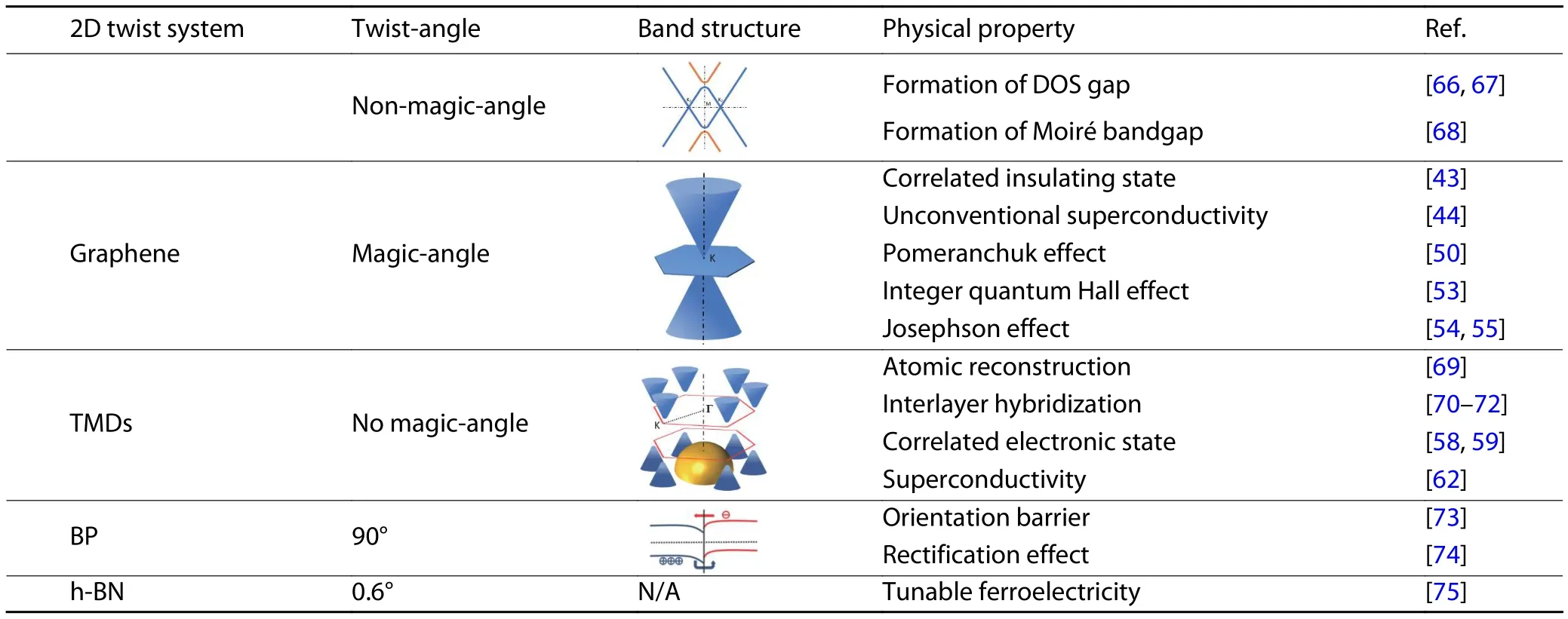
Table 1.Primary 2D materials for twisting with their typical band structure and important physical properties.
It is well known that artificially controlling the twistangle between two stacked materials actually violates the lowest energy principle of the whole system, especially some weird angles like the magic angle.One-step CVD under special conditions could produce twisted layers but with uncontrollable as well as random twist-angles[76].Therefore, typical fabrication methods to obtain twist-angle 2D superlattices can be regarded as a combination of synthesizing two parts respectively and stacking them together.Firstly, almost every technique to fabricate common 2D materials which include CVD (usually low pressure)[66,67,77], mechanical exfoliation[54,74,78]and epitaxial growth is able to produce the components.Then, the crucial process is to compact the components together to form a twisted superlattice.In this step, dry transfer containing tear and stack[68,75,79,80]or hot pick-up,wet transfer by coating transfer mediate like PMMA[78]are commonly used, analogous to fabrication of normal heterostructures but with an additional twisting.Sometimes femtosecond laser cuts would be employed to tailor the raw materials, enhancing its in-plane anisotropy[73].The above routes can be described by the following schematic figure which only shows comprehensive steps (Fig.2).
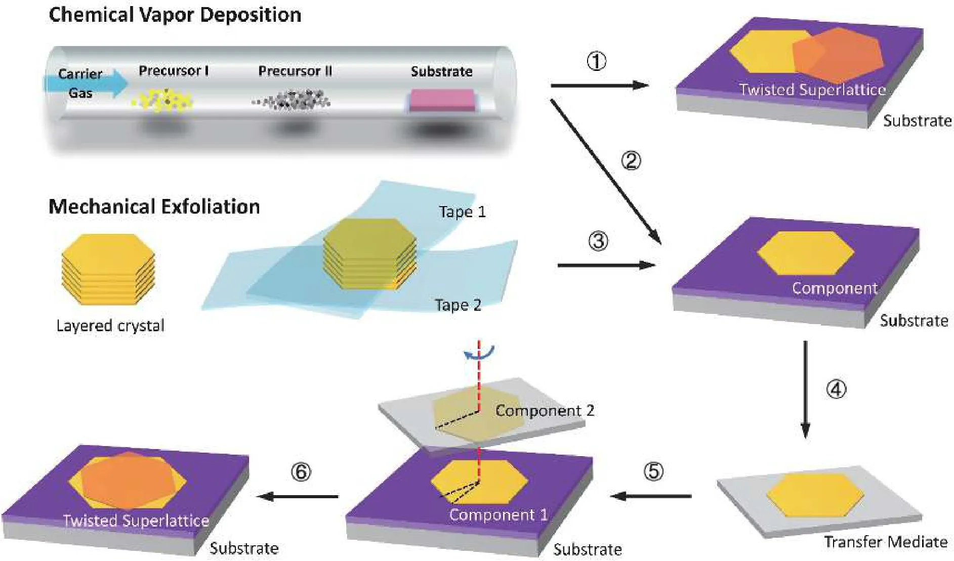
Fig.2.(Color online) Fabrication methods and synthesis routes of twist-angle 2D superlattices.① One-step growth of twisted superlattice by chemical vapor deposition; ② Fabrication of component 1 (single-layer or several layers) by CVD; ③ Fabrication of component 1 by mechanical exfoliation; ④ Transfer of the product from synthesis substrate to device substrate by dry or wet transfer methods; ⑤ Adjusting the twist-angle of component 1 and component 2 which stay on device substrate and transfer mediate respectively; ⑥ Compaction of component 1 and component 2 to form twist-angle 2D superlattice.
When increasing progress has been made in exploring electronic structure changing, interlayer coupling and excitonic behavior in the twisted 2D systems, relevant applications in microelectronics and optoelectronics, such as rectifying and response to incident radiation, have also obtained increasing concerns.In this article, we dominantly focus on twistangle two-dimensional superlattices and their applications in(opto)electronics.Some representative works containing versatile applications (i.e., photodetector, diode, field-effect transistor, Josephson junction…) and diverse materials (i.e.,graphene, TMDs, BP, h-BN) will be exhibited.Therefore, Moiré pattern, interlayer coupling and interlayer exciton behaviors in different 2D materials will be discussed primarily.Then,twist-angle-dependent Moiré bands and anisotropy of the twisted superlattice will give rise to tunable (opto)electrical properties, resulting in versatile applications including a transistor,rectifier, photodetector and light emission diode.
2.Moiré superlattice
Because of the convenient operation and superior controllability of twisting, which can maintain intrinsic features and bring novel properties simultaneously, twist-induced Moiré pattern in the superlattice became an outstanding platform for study on twist-angle-dependent properties[32,81,82].It is well known that when two 2D lattices with similar periodicity and pattern are stacked followed by twisting relatively, the Moiré superlattice will be formed in which new periodic units with several orders of magnitude larger area will replace the intrinsic unit to bring new periodicity but similar shape of repetitive cell to the bilayer system (Fig.3(a)), followed by the presence of Moiré potentials as substitution for pristine crystal potential, shown in Figs.3(b)–3(d).

Fig.3.(Color online) Moiré superlattices, interlayer coupling and the behavior of interlayer excitons in Moiré potentials.(a) Twist-angle-dependent Moiré pattern of TBG.Reproduced with permission[86].Copyright 2015, American Physical Society.Mapping of potential difference in ABAB and ABCA stacking modes (top) and potential fluctuation along the certain direction marked by red color (bottom) measured by amplitude modulated scanning Kelvin probe microscopy (AM-SKPM) (b) and frequency modulated SKPM (FM-SKPM) (c), respectively.Reproduced with permission[84].Copyright 2021, American Chemical Society.(d) Schematic of Moiré potentials resulted from Moiré pattern, containing saddles and wells.Reproduced with permission[45].Copyright 2018, American Physical Society.(e) Moiré superlattice of rigid-lattice MoSe2/WSe2 at 0°+δ.(f) Theoretical calculation of stacking energy, showing an identical energy of AB and BA stacking modes.(g) The evidence of superlattice reconstruction based on observed alternant triangular regions; while rigid-lattice pattern of MoSe2/WSe2 at 60°+δ theoretically showed similar smoothly boundary (h), and hexagonal reconstruction (j) resulting from the single minimum of stacking energy reduction in ABBA mode (i).Reproduced with permission[69].Copyright 2020, American Chemical Society.
When focusing on the detailed atomic arrangement in twisted 2D systems, it is notable that small domains inside a Moiré periodicity possess versatile stacking modes.Compared to uniform Bernal stacking (AB stacking) in bilayer graphene without twisting, TBG exhibits much more complex and diverse stacking modes including AA, AB, BA, SP…,which are typically shown as alternately triangular or hexagonal regimes with interval domain walls[83,84].For TMDs with a sandwich structure and honeycomb lattice, AA, AA’, AB and BA, AB’ and A’B in different regimes of twisted bilayer TMDs(TBTMDs) have also been observed in the Moiré pattern.However, due to steric effect from chalcogenide atoms like sulphur and local strain distribution, atomic reconstruction always takes place to rearrange atomic configurations, resulting in energy-favorable AA’, AB and BA stacking with distinct domain walls rather than smoothly blurry boundaries according to rigid lattice hypothesis[69,85](Figs.3(e) and 3(h)).Owing to sixfold rotation symmetry both in TBG and TBTMDs,meaningful information can be obtained by tuning twistangle just from 0° to 60°.Thus, considering atomic reconstruction and the lowest energy principle, triangular domains occupied by AB and BA stacking with clear boundaries rather than smooth varying were clearly observed when twist-angle was tuned close to 0°, providing convictive evidence for atomic reconstruction (Figs.3(f) and 3(g)).And when twist-angle was reaching 60°, AA’ stacking replaced AB and BA modes to become a dominant mode and led to hexagonal domains(Figs.3(h) and 3(j)).But different with TBG, Moiré patterns in TBTMDs seem much more intricate, especially considering the difference between homo- and hetero-structures.For instance, MoSe2/WSe2or MoS2/WS2heterostructure with triangular AB/BA periodicity would form I-type band alignment, resulting in higher carrier concentration in BA domains which can be testified by photoluminescence (PL) spectra.However, in the ~60° twisted MoS2bilayer homostructure, AA’ stacking regimes with Reuleaux triangular shape, rather than the expected hexagonal shape, would act like quantum wells, resulting from the additional modulating confining potential and multiple discrete flat bands at conduction and valence band edges[85].
On one hand, owing to the different spatial configuration in different stacking modes, carriers moving in the Moiré superlattice will feel like a different chemical environment, resulting in the imparity of electronic structure and the presence of periodic Moiré potentials in real space which will exert great influence on carrier transportation (Figs.4(a) and 4(b)).On the other hand, from the perspective of momentum space, the Moiré superlattice with a much larger scale is corresponded to smaller Brillouin zone due to the reciprocal relation between real space and momentum space[87],hence tailoring the pristine band structure and modifying the interlayer coupling through creating hybridization among the bands from individual layers.

Fig.4.(Color online) (a) Moiré periodic potential wells formed in MoSe2/WSe2 twisted heterostructure which would influence the transport process of excitons.(b) Localized excitons in Moiré periodic potential wells at ultra-low temperature of 4 K.Reproduced with permission[88].Copyright 2021, American Chemical Society.(c) PL spectra of monolayer and twisted bilayer WS2 with various twist-angles.(d) The position of PL peaks of A (red dots) and I (blue dots) at various twist-angles.(e) and (f) are the E2g and A1g peaks in Raman spectra with different twist-angle,which reflect intralayer vibration and interlayer vibration, respectively, being summarized in (g).(h) The distance between E2g and A1g peaks as a function of twist-angle, indicating the interlayer coupling strength.Reproduced with permission[89].Copyright 2019, American Chemical Society.
Actually, the Moiré superlattice was seen as the ideal platform to investigate exciton behaviors a long time ago, typically using PL spectra to check the excitonic energy (Figs.4(c)and 4(d)) and Raman spectrum to testify the interlayer coupling (Figs.4(e)–4(h).In 2014, Liuet al.[72]employed second-harmonic generation (SHG) to check the twist-angle of twisted bilayer MoS2and analyzed the strength of interlayer coupling through two phenomena, the splitting of degenerated valence band at Γ point termed as “hybridization Γ band” and the interlayer excitonic relaxation process.It was demonstrated that the distance betweenpe aks was usually used as evidence for judging the thickness of the TMD sheet[90], representing the interlayer coupling strength and varying with the twist-angle which determined the interlayer distance by steric effect from Sulphur atoms.This interlayer coupling strength was in good agreement with the position of interlayer excitonic PL peaks, in which the hybridization Γ band would be closer to the conduction band minimum(CBM) at K point with the increment of the interlayer coupling strength, leading to the corresponding PL peak appearing at lower energy position.If replacing homobilayer TMDs by heterostructures like MoS2/WSe2, interlayer excitonic relaxation showed totally different PL energy with single-layer counterparts, but similar relaxation routes that are from CMB at K point to the hybridization Γ band[71], which was further confirmed by Kunstmannet al.[70]in 2018 using the same materials with the help of temperature controlling.
Intriguing phenomenon in the PL spectrum implied attractive exciton behaviors in the Moiré superlattice.In 2018, the arcane Moiré potentials and the behavior of Moiré-potentialtrapped excitons were detected experimentally in twisted MoSe2/WSe2heterostructures by Seyleret al.[91].During the exploration of detailed factors affecting the Moiré potential barriers, Shabaniet al.[92]falsified the previously accepted monotonic relation between Moiré potential and Moiré periodic length and found the maximum of Moiré potential could be achieved at a Moiré periodicity around 13 nm.It was suggested that the reason why Moiré potential in experimental measurements was usually much larger than theoretical calculation could be that Moiré potential was dominantly determined by the Moiré structure and internal strain instead of interlayer coupling.In 2021, Andersenet al.[93]observed polarization-selective response of the doped excitons in twisted WSe2bilayers by injecting charge carriers into certain stacking regimes through the electric field, giving rise to promising applications in quantum optoelectronics.In the same year, the exciton behavior in monolayer/bilayer phosphorene was also found to be strongly dependent on twistangle.Zhaoet al.[94]revealed the modulation of band structure and optical transition process by twisting monolayer phosphorene relatively to the bilayer, through photoluminescence excitation spectroscopy (PLE) and first-principles calculation.It was elucidated that the influence from Moiré superlattices remained even when the twist-angle was increased to 19°.
In short, twisting, as a new freedom degree of adjusting properties of the twist-angle 2D systems, not only tailors the electronic structure of charge carriers inside but also creates Moiré potential to change the exciton behavior.Therefore,for a twist-angle 2D Moiré superlattice, band structure, photoinduced transition routes, interlayer coupling strength and periodic potential field can all be easily tuned by twist-angle combining with external electric or magnetic field, indicating the twisted system is a significantly promising candidate for applications in (opto)electronic devices.Hence, some realized achievements and theoretical predictions will be discussed later in this article.
3.Graphene-based devices
Graphene, as the first discovered and the most popular 2D material, has owned abundant attention on its twistronic properties, hence going the farthest in applications among oth-er twisted 2D counterparts.
Since the atomic thickness endows transparency to graphene, the low photoresponsivity partially caused by the low photon absorption ~2.3% and the inferior selectivity(from ultraviolet to infrared) become a bottleneck for optimizing monolayer graphene-based photodetectors.Therefore, in 2013, Baoet al.[95]proposed that if we want to improve photoresponsivity but preserve high carrier mobility in graphene, it seemed a feasible way to use CVD followed by exfoliation to produce large-area (~100μm) TBG with relatively large twist-angle, in which Dirac cone structures could be retained but creating new bands at the intersection points of the merging Dirac cones.
In 2016, considering the twist-angle-dependent band structure, Yinet al.[66]fabricated a TBG photodetector with a twist-angle of 13° and obtained a ~80 times enhancement in photocurrent under incident radiation with a certain wavelength with the help of integration of plasmonic structure in the device.The relatively large twist angle rendered both the conservation of Dirac cone structure and the merging of two Dirac cones from top and bottom layers (Fig.5(a)).A gap occurred at the intersection of two merging Dirac cones observed by micro-ASPES, leading to the presence of VHSs in DOS (Figs.5(b)–5(e)).It is found that the energy difference between Fermi level and VHS (defined asEVHS)changes with the variation of twist-angle (Fig.5(f)), generating an excitation route through the gap of 2EVHSat the intersection of the merging Dirac cones when the photon energy matches well with the DOS gap.
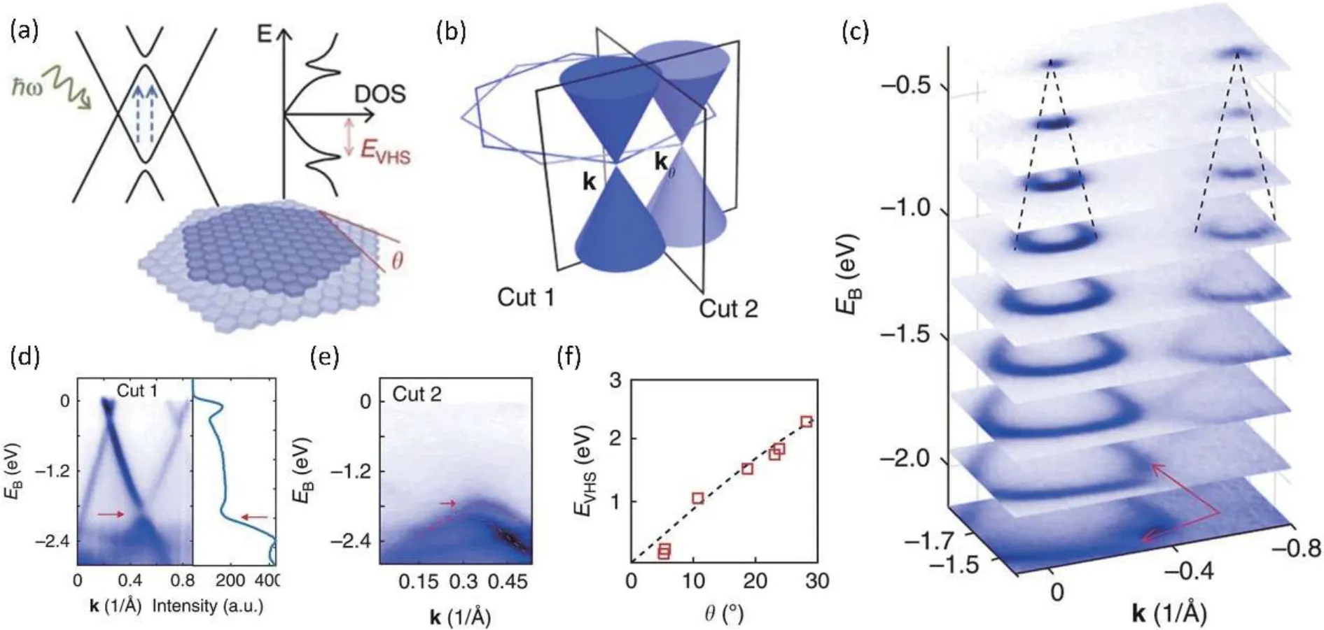
Fig.5.(Color online) The merging of two Dirac cones and the presence of DOS gap.(a) The DOS gap is established between two VHSs and hence create the photoexcited transition route.(b) Schematic of the merging Dirac cones with other two operating directions of ARPES spectra to the TBG.(c) Stacking plot of constant-energy contours measured by ARPES, showing the merging of Dirac cones.The band structures in Cut 1 and Cut 2 from (b) are shown in (d) and (e), respectively, where VHSs are marked by red arrows.(f) DOS gap (2EVHS) as a function of twist-angle.Reproduced with permission[66].Copyright 2016, The Author(s).
After obtaining TBG with various twist angles by CVD growth on copper foil and subsequently transferred to the SiO2/Si substrate, a photodetector was fabricated with two regimes in which bilayer graphene were 7° and 13° twisted, respectively (Figs.6(a) and 6(b)).Then a significant enhancement of Raman G-band intensity and photocurrent in 13°TBG than 7° was observed when being shined by incident light with a wavelength of 532 nm (2.33 eV), which can be attributed to the well matching of the gap value (2EVHS= 2.34 eV in TBG at 13°) with incident photon energy (Figs.6(c) and 6(d)).It was evidenced by the fact that the photoresponsivity of 13° TBG under 532 nm, which reached 1 mA/W, was nearly seven-fold larger than that of 7° TBG.By changing the twistangle, TBG exhibited a strong photocurrent to incident light with different certain wavelength, indicating the selectivity in photoresponsivity was achieved by twisting (Fig.6(e)).
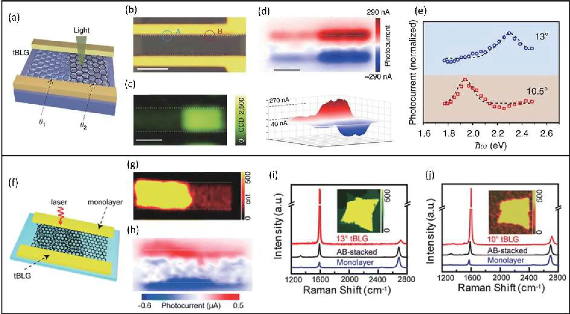
Fig.6.(Color online) Selectively enhanced photoresponsivity of TBG based on a tunable DOS gap.(a) Schematic of a TBG-based photodetector whose channel consists of two TBG with different twist-angle of θ1 = 7° and θ2 = 13°, respectively.(b) The corresponding optical image of the device in which the dashed circle A and B represent 7° and 13° regimes.(c) Raman G-band intensity mapping under a 532 nm (2.33 eV) laser.(d)Scanning photocurrent distribution of the same device in planform (top) and stereogram (bottom).(e) Twist-angle-dependent the position of photocurrent maximum peaks responding to different photon energy.Scale bars: 5 μm (all).Reproduced with permission[66].Copyright 2016, The Author(s).(f) Schematic of the device consisting of TBG at 10° and monolayer graphene.(g) Raman G-band intensity mapping of the same device under 633 nm (1.96 eV) laser.(h) Scanning photocurrent distribution of the device in which strong photoresponsivity almost took place in the TBG region.Significantly enhanced G-band intensity in Raman spectra of 13° TBG under 633 nm laser (i) and 10° TBG under 532 nm laser (j), respectively.Reproduced with permission[67].Copyright 2016, American Chemical Society.
In the same year, this group improved synthesis method by combining CVD with PMMA transfer in order to obtain large-domain TBG with the size around 100μm (Fig.6(f)).For verifying the correlation between enhancement in the selectivity of photoresponsivity and the DOS gap in Moiré bands,Tanet al.[67]further tested another twist-angle of 10° whose DOS gap of 2EVHSwas well matched with the photon energy of 633 nm wavelength (1.96 eV) and found an expectable~20-fold enhancement in Raman G-band intensity (Figs.6(g),6(i)–6(j)) and a ~6 times increment in photocurrent compared with monolayer counterpart, giving rise to the achievement of photoresponsivity of 2.5 mA/W (Fig.6(h)).Through stacking two graphene layers with a twist, light-matter interaction could be drastically improved, resulting from the construction of photoinduced transition routes between VHSs.
Similar to Zhongfan Liu’s work, Xinet al.[78]also employed TBG with a twist-angle of 10° and 12° tested by light with a wavelength of 633 and 532 nm, respectively.The incident radiation was shined on left and right electrodes with different incident angle and polarization phase (Figs.7(a)and 7(b)).Benefiting from surface plasmon resonance in metal–graphene–metal architecture, TBG in the vicinity of the metal-TBG interfaces, showed further enhanced photoresponsivity with spectral selectivity and a seven-fold increment of photovoltage.It was elucidated that the photoresponsivity in 10°-TBG under 633 nm radiation with 48° polarization and 12°-TBG under 532 nm radiation with 52° polarization could be maximized to 2.2 and 1.6 V/W, respectively.Hence, for TBG with a certain twist-angle under optimal incident laser,both the incident angle and polarization phase would influence the induced photovoltage, shown in Figs.7(c)–7(f),providing a geometric optimizing idea for designing photodetectors with higher photoresponsivity in the future.
Photoresponsivity in the terahertz (THz) range with polarization-sensitivity to different twist-angles was theoretically predicted in twisted bilayer graphene quantum dots (GQD) in 2019 by Tiutiunnyket al.[96].Strictly, electronic structure in GQDs exhibited dense molecular orbitals rather than quasi-continuous band structure, but the photoexcited transition from HOMO to LUMO showed a resembling principle with TBG,hence also having the potential to be utilized in DOS gap engineering.When the size of graphene sheets was reduced to several nanometers, the electronic structure would be determined by twist-angle, size and the edge morphology of GQDs which could be categorized into zigzag-triangular-GQD (ZTGQD), armchair-triangular-GQD (A-TGQD) and circular-GQD(CGQD) (Fig.7(g)).For example, the gap between LUMO and HOMO in Z-TGQDs could be narrowed and finally closed by increasing twist-angle under an external electric field, giving rise to potential applications in the THz detector (Figs.7(h)and 7(i)).As for small A-TGQDs, the difference in photoresponsivity to polarized light with different polarization direction could be magnified with the increment of twist-angle.Al-though the physical meaning remains unveiled, integrated array based on GQDs could be a potential optoelectronic sensor in practice.
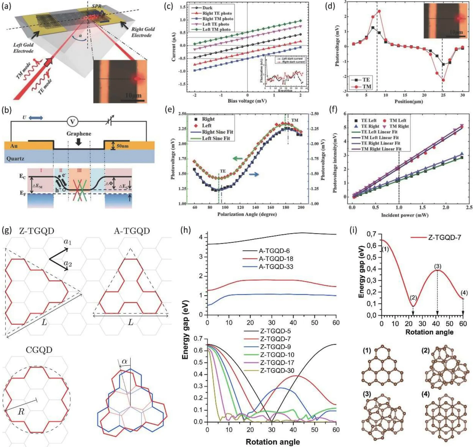
Fig.7.(Color online) (a) Schematic of a TBG-based photodetector with metal–graphene–metal architecture (MGM), and the inset shows a zoom of the central region at the MGM junction.(b) Model of the device and the corresponding energy structure.(c) Current as a function of bias voltage of TBG at 10° at the left and right side under different polarized radiation, and the inset is the dark current fluctuation.(d) Different photovoltage of 10° TBG under lasers with different polarization modes.(e) The photovoltage as a function of polarization angle at the left and right MGM junctions with sine fitting.(f) The linear relationship between incident power and photovoltage intensity at different positions under different polarized lasers.Reproduced with permission[78].Copyright 2016, WILEY-VCH Verlag GmbH & Co.KGaA, Weinheim.(g) Three types of graphene quantum dots and twisted bilayer graphene quantum dot.(h) Energy gap as a function of rotation angle for A-TGQD with different size (top) and for Z-TGQD with various size (bottom).(i) Further analysis on Z-TGQD-7 on twist-angle-dependent energy gap (top) and the model of stacking configurations at four rotation angles (bottom).Reproduced with permission[96].Copyright 2019, Elsevier B.V.All rights reserved.
Actually, the terahertz photo-galvanic response was realized earlier in the TBG photodetector instead of twisted GQDs.In 2020, Ottenederet al.[79]observed oscillations of resistance and photocurrent in a ten-terminal measurement made by the encapsulated TBG with a twist-angle of 0.6°(Fig.8(a)), which can be attributed to the synergy of ultrasmall twist-angle and gate bias.It was suggested that the voltage responsivity reached 80 mV/W under 432μm THz radiation.More importantly, polarization (azimuth angleα)played an essential role in the determination of photovoltage which was given bywhereUL1,UL2andU0are fit coefficients, serving as different weights to Stokes parameters cos2αand sin2α(Figs.8(b) and 8(c)).This expression provided a reasonable explanation to polarization-dependent photoresponsivity at certain twistangles.It is obvious that linearly polarized radiation combining with gate bias could change both the magnitude and direction of photocurrent, which has also been realized by exerting right-circularly and left-circularly polarized radiations(Fig.8(d)).The fluctuation of the photocurrent with gate bias also provided evidence for the presence of multiple separated mini-flat-bands.It was implied that when the Fermi level shifted across those separated flat bands by controlling gate bias, density of states of the system was oscillated in turn,which resulted in the oscillation of resistance and finally the magnitude of the photocurrent.This result revealed that gate bias may act as far more than a depression of the dark current, but a controller of photoresponsivity.
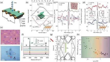
Fig.8.(Color online) (a) Schematic of a TBG-based Terahertz photodetector.(b) Photovoltage as a function of the azimuth angle of the incident light.(c) Fluctuation of photovoltage intensity caused by a tunable filling level of the multiple relatively flat bands through gate bias.(d) Gate-bias-dependent circular photovoltage at bulk (offset by 90 nV/mW for visibility) and edge, and longitudinal resistance under the control of gate bias.The top two inset images are polarization-dependent photovoltage signals and the bottom inset shows an experimental measurement.Reproduced with permission[79].Copyright 2020, American Chemical Society.(e) Optical microscope image of star-like TBGs (top) and the image of the one marked by the black arrow (bottom), in which colorful circles represent TBG with different twist-angle and the black circle represents monolayer graphene.(f) Significantly enhanced G-band intensity in Raman spectra of the green region under 532 nm laser, indicating the TBG at around 12°.(g) Schematic of band structure and third-harmonic generation process when the DOS gap matches well with the three-photon energy.(h) Tendency of THG intensity with respect to I2D/IG ratio.Reproduced with permission[76].Copyright 2021, The Author(s).
The enhanced light-matter interaction in TBG unveiled by Yinet al.[66]reminded researchers of another potential application, optical nonlinearity.After observation of tunable second harmonic generation in TBG by Yanget al.[80], recently, Haet al.[76]successfully grew the star-shape TBG in which diverse twist-angle could be obtained in different regimes and observed expected strong Raman G-band intensity in 12° TBG under 520 nm laser (Figs.8(e) and 8(f)).Subsequently, enhanced third-harmonic generation (THG) was achieved by shining incident light with 1560 nm wavelength on TBG with a twist-angle of 12° owing to the three-photon transition process described in Fig.8(g).Such an optical nonlinear process became evidence for the presence of strong light-matter interaction.Furthermore, the following observations verified twist-angle as a critical free-degree to control the system.Once external electric field carried out by gate voltage broke the symmetry of Moiré bands and resulted in imbalance in electron and hole branches, then parallel band transition would be badly disturbed, followed by normalized THG intensity decreased (Fig.8(h)).But for those TBG with twist angle a little bit smaller or larger than 12°, the symmetry-broken Moiré band would instead help to create a suitable energy gap between two shifted VHSs and generate strong optical nonlinear response.More importantly, secondand third-harmonic generation always serve as a technique to distinguish the direction of crystal grain, which is helpful in recognizing the twist-angle experimentally.
It was fully evident that aforementioned studies utilized twisting to promote the merging between two Dirac cones in order to obtain VHSs in DOS which played a critical role in optimizing the interaction of light and matter.In addition, twistangle-dependent Moiré bandgap between Moiré Dirac bands and upper (or lower) bands will offer another way to introduce transition processes.
Different with relatively large twisting, Denget al.[68]only twisted the bilayer graphene with a small angle of 1.81° to build a photodetector which exhibited strong photoresponsivity in mid-infrared range.Rather than engineering the DOS gap in the merging Moiré Dirac band, small twist-angle created superlattice Moiré bandgap in electron and hole branches, respectively.It was such a bandgap that made it possible for photoexcited interband transition, hence improving the photoresponsivity.Besides, it led to optimal photon absorption when the incident photon energy resembled with the gap due to the preferable band edge transition.
For a photodetector made by 1.81° TBG, light-matter interaction could be significantly enhanced through bolometric effect under incident light with a wavelength of 12μm than 5.0 and 7.7μm.It was observed that the photoresponsivity reached 26 mA/W under 1200 nm radiation when the Fermi level was tuned in the center of the superlattice gap under gate bias of 43.5 V.Similarly, when the gate bias was adjusted to –43.5 V, indicating the Fermi level was tuned in the gap of hole branch and the Moiré band was vacated, photoresponsivity and sheet resistance also reached a maximum.Otherwise, responsivity and resistance would decrease fast, resulting from the metallic behavior when the Moiré band was half-filled sinceEFwas positioned in the superlattice band.However, it was notable that such strong photoresponsivity finally disappeared with continuously decreasing twist-angle due to the close of superlattice bandgap.
When we pay attention from photoexcited transition to the tunable band structure in TBG itself, it reminds of the possibility in electronic applications.The requirements for electronic devices are totally different from optoelectronics because bandgap engineering will make a limited contribution to electric properties like current rectifying but tunable band structure provides an idea to break band symmetry to generate anisotropy in effective mass by exerting external fields.
In 2021, Liuet al.[97]utilized twisting of 1.5° and external magnetic field of 10 T to respectively break the spatial inversion symmetry and the time-reversion symmetry of TBG, in order to induce giant unidirectional magnetoresistance through breaking the symmetric band structure (Figs.9(a)–9(c)).In a two-terminal measurement, unidirectional magnetoresistance (UMR) was defined to describe the rectifying effect, given by, where ΔR, R,v←andv→represent the difference of magnetoresistances along opposite direction, the sum of magnetoresistance along the opposite direction, the Fermi velocity along left direction and the Fermi velocity along the right direction, respectively.It was found that the UMR of such a system could achieve 22% by improving the value of disparity betweenv←andv→and enhancing the DOS through optimizing the direction of external magnetic field to parallel with the current direction in plane and tuning the twist-angle to 1.5°, respectively (Figs.9(d)–9(g)).Theoretically, the UMR realized in this work revealed the potential in developing rectifier or chirality probing based on the TBG system.
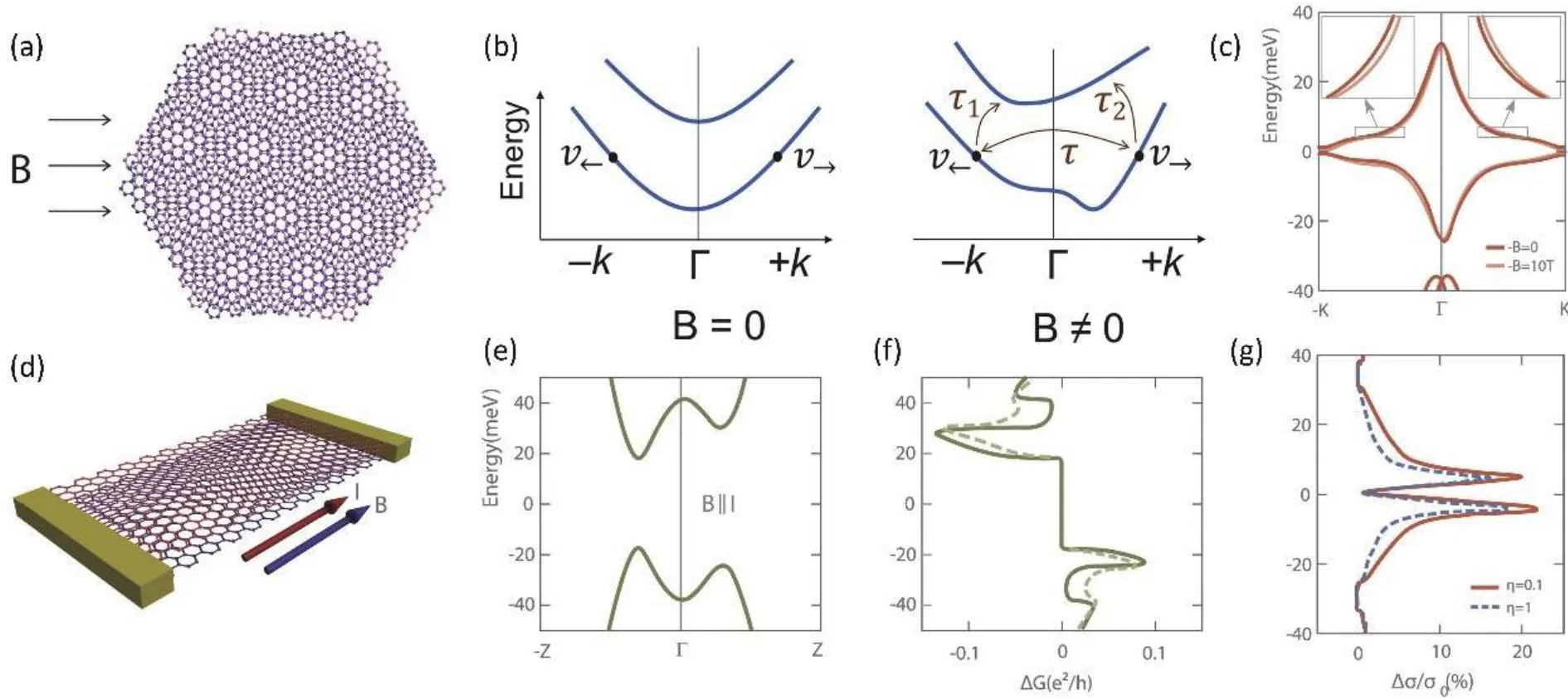
Fig.9.(Color online) Chirality-induced giant unidirectional magnetoresistance in TBG at 1.5°.(a) In-plane external magnetic field will break the time-reversion symmetry on the TBG with chirality caused by twisting, leading to band structure changing from symmetric (b, left) to asymmetric (b, right) and unidentical carrier velocity along the opposite direction.(c) The band structure of TBG under 10 T magnetic field (orange line)and without magnetic field (red line).(d) Schematic of the device under in-plane I//B.Electronic structure of the TBG in the case (d) and corresponding direction-induced conduction difference ΔG=G→−G←(f).(g) Calculated unidirectional magnetoresistance at η = 0.1 (blue dashed line)and 1 (red solid line), respectively, where η is dephasing parameter.Reproduced with permission[97].Copyright 2021, The Authors.
When magic-angle twisted bilayer graphene (MATBG) is paid attention from the investigation of physical properties to the implementation of practice, the gate-tunable superconductor and insulator phases in such single-material platform are seen as critical serviceable properties in quantum electronic devices.In 2021, both Rodan-Legrainet al.[55]and de Vrieset al.[54]successfully fabricated a MATBG-based Josephson junction but with different architecture, which is a widely used quantum superconducting electronic device that typically consists of two superconductors separated by an ultrathin insulator, and even serves in the definition of standard unit Volt by National Institute of Standards and Technology, USA.de Vrieset al.[54]designed a four-gate measurement with three top gates and one graphite bottom gate to precisely control the electronic states in different regimes of MATBG at 1.06° and observed direct-current as well as alternating-current Josephson effects, verifying the high-quality formation of a single-material 2D Josephson junction.Compared with the multi-gated architecture, Rodan-Legrainet al.[55]proposed two kinds of device structures named as device A and B which contained a narrow top gate and two separated top gates, respectively,but both equipped with a large-scale bottom gate.Device A was employed to obtain versatile contacts in the MATBG at~0.95° including SIS, SSS, SCS, SDS… where S, I, C and D is the short term for superconducting, insulating, correlated insulating and charge-neutral Dirac point phases, respectively.Therefore, operationally analogous to the doping technique in producing a n-type semiconductor in a bulk p-type semiconductor, the narrow top gate in this study exerted similar influence to tune the electronic states in the region underneath to fabricate the ultrathin insulator barrier between two largescale superconductors.More splendidly, they further observed a Coulomb blockade with uniform Coulomb diamonds in device B, indicating that a single-electron transistor was formed when both left and right regimes were adjusted into metallic phases while leaving the interval region as an isolated island.Moreover, it was demonstrated that in agreement with the aforementioned work[43,44], thermal fluctuation and external magnetic field would drastically disturb the Josephson effect and Coulomb blockade through breaking the superconducting as well as insulating states inside MATBG.These two very recent works shed light on the possibility and feasibility of applications in electronic devices of more Moiré systems due to some confirmation of the existence of similar flat bands and electric field modulated electronic states in TBTMDs.
4.Other 2D material-based devices
4.1.Transition metal dichalcogenides
Compared with graphene, which possesses linearly dispersed electronic structure and non-gap feature, other 2D materials like TMDs and BP that typically have considerable bandgaps are naturally suitable candidates for applications in electronic and optoelectronic devices.It is known that anisotropy in a crystal structure would be reflected in electronic structure, leading to anisotropic carrier transportation and polarization-sensitive photoresponsivity.But such anisotropic properties can be tuned by band engineering through twisting.For instance, BP, a famous anisotropic 2D material firstly fabricated by Liet al.[16], has been found to have a distinct difference in carrier transport properties between along zigzag and armchair direction.However, after being stacked by another BP sheet with a relative twist-angle, the anisotropy in this bilayer system will be adjusted, indicating tunable electrical properties.Analogously, the twist-angle-dependent interlayer coupling strength and interlayer excitonic behavior in TBTMDs implies the possibility for applications in (opto)electronic devices.
In 2019, Choiet al.[98]testified the relationship between optoelectrical properties and interlayer coupling strength modulated by twisting.And they found that vertically stacking MoSe2and WSe2with a twist-angle of 15° and 30° would significantly influence the interlayer coupling between two semiconductor sheets and hence increase the difficulty for carriers to go across the heterostructure, indicating the construction of an equivalent transport potential barrier in between and the gradual decoupling process of two layers (Figs.10(a)and 10(b)).Such a decreasing interlayer coupling strength, as well as the subsequent transport potential barrier, however,widen the bandgap thus giving rise to the enhancement of both spectral responsivity and external quantum efficiency(EQE) under ultraviolet (365 nm) luminescence (Figs.10(c)–10(f)).But for homojunction like a 30° twisted MoS2bilayer in which there was no natural interlayer work function difference.Liaoet al.[77]found that it exhibited better rectification property with higher on/off ratio of 108, an order of magnitude larger than the untwisted counterpart, attributing to the higher on-current (Figs.10(g)–10(i)).Owing to the interlayer decoupling by an incommensurate structure at a twistangle of 30°, interlayer resistance was reduced and resulted in a higher field electric mobility than both the untwisted bilayer and the (0°, 30°)/(30°, 0°) trilayer, where (0°, 30°) indicated the two relative twist-angles between each two layers in the trilayer system are 0° and 30°, respectively (Fig.10(j)).Therefore, twist-angle-dependent interlayer coupling strength would be an important access to optimize the transport property of TBTMDs, requiring further exploration.
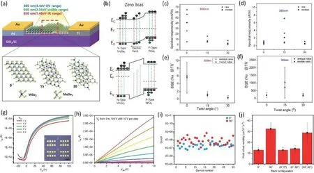
Fig.10.(Color online) Weakened interlayer coupling of TBTMDs and optimized rectifying behavior.(a) Schematic of a bilayer heterojunction WSe2/MoSe2 with different twist-angle including 0°, 15° and 30° under incident light with various wavelengths.(b) Band structure of 0° (top row)and 15° (bottom row) WSe2/MoSe2 bilayer heterojunction under zero bias.(c) and (d) show spectral responsivity with raw and median values of three devices with 0°, 15° and 30° under IR (850 nm) and UV (365 nm) luminescence, respectively.(e) and (f) show external quantum efficiency(EQE) with average and median values of the three devices under 850 nm and 365 nm radiation, respectively.Reproduced with permission[98].Copyright 2019, American Chemical Society.(g) Electrical transfer curves of a 30° twisted bilayer MoS2 field effect transistor, the inset is the optical image of the device array, scalebar is 400 μm.(h) Electrical output curves of a 30° twisted bilayer MoS2 FET.(i) The statistic distribution of the on/off ratio of 30° (red dots) and 0° (blue dots) twisted bilayer MoS2 FET.(j) Field effect mobility measured in twisted bilayer and trilayer MoS2 FET, where 0° and 30° represent the twist-angle in bilayer sample and (0°, 30°) means two relative twist-angles between each two layers are 0°and 30°, respectively, in a trilayer system.Reproduced with permission[77].Copyright 2020, The Author(s).
Similar to optical nonlinearity in TBG including enhanced second- and third-order harmonic generation, TBTMDs have also been discovered controllable matter-light interactions with cavities in strong coupling regimes.The interlayer excitons confined in Moiré potential wells in MoSe2/WS2heterostructure at the temperature of liquid-nitrogen gave rise to strong nonlinearity, resulting in the density-dependent Moiré polaritons, which could be utilized as tunable arrays of quantum emitters by using long-range light coherence and cavity engineering[99].
4.2.Black phosphorus
As for other twisted bilayer 2D materials like BP, there have been some valuable experimental data and relevant explanatory theories but most investigations have still been concentrated on theoretical simulations so far, providing meaningful information and bright prospect for approaching studies.It was generally acknowledged that the structural anisotropy along zigzag- (ZZ) and armchair-direction (AC) in BP was regarded as the origin of its intriguing optical polarization-sensitive and rectification properties.In other words, if one can control the anisotropy in BP, it will be prospective for BP to act as an ideal candidate for both the controllable photodetector and diode.Fortunately, single twisting without heteroatomic doping or other complex treatment could achieve the goal,verifying the effectiveness of the new freedom level, twist angle, to 2D systems.
In 2016, Caoet al.[100]calculated on the band structure of twisted bilayer BP (TBBP) at 90° and observed disappearance of anisotropy in the perpendicularly stacked TBBP system which was corresponded to the new symmetric band structure along Γ–Y and Γ–X’ (Fig.11(a)).More interestingly, such band symmetry could be broken by exerting external electric field (gate bias), hence regaining the asymmetry of the band dispersion and the difference of hole effective mass along the two perpendicular directions, which implied a gate-dependent anisotropy can be formed by cross-stacking(Fig.11(b)).Furthermore, tunable anisotropy in TBBP theoretically brought polarization-sensitivity to the system, firing the enthusiasm on exploring practical devices for application in(opto)electronics.
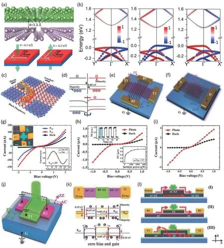
Fig.11.(Color online) (a) Schematic of a cross-stacked bilayer black phosphorus (BP).(b) Significant influence on the effective mass of holes along zigzag and armchair direction in BP under external electric field.Reproduced with permission[100].Copyright 2016, American Chemical Society.(c) The schematic of cruciform few-layer BP (CBP) device without twisting but adjacent electrodes connected.(d) The difference in the band structure and Fermi levels along AC and ZZ directions induced by anisotropy in BP (top) and the formation of orientation barrier from the bands bending (bottom).(e) Cross-stacked few-layer BP junction (CBPJ) with adjacent electrodes connected.(f) Vertical-stacked BP (VBP) with only two opposite terminals connected.(g) Photoresponse under incident light with polarization state along the AC (red) and ZZ (blue) direction and intrinsic rectification curve (black).The top-left inset showed an optical image of the CBP device while the bottom-right inset showed the polarization-dependent photocurrent.(h) Photoresponse (red) and intrinsic rectification features (black) of CBPJ.The top-left inset showed millisecondlevel photoresponse under pulse light while the bottom-right inset revealed incident-power-dependent photocurrent with photoresponsivity of 4.6 mA/W at 50 μW.(i) Photoresponse (red) and intrinsic rectification features (black) of VBP under incident light with certain polarization state.Reproduced with permission[73].Copyright 2017, WILEY-VCH Verlag GmbH & Co.KGaA, Weinheim.(j) Schematic of a vertically cross-stacked BP junction under laser illumination.(k) Top: schematic of the top view of B1-B2 two terminal device; middle: pristine energy band and Fermi level distribution with bandgap of 0.57 eV; bottom: after thermodynamically equilibrium, a p-p-p lateral junction was formed with orientation barrier of 0.05 eV.(l) The stacking-morphology-dependent carrier transportation processes.Reproduced with permission[74].Copyright 2018, WILEY-VCH Verlag GmbH & Co.KGaA, Weinheim.
One year later, in 2017, Xinet al.[73]in Jian-guo Tian’s research group designed three types of architecture of BP devices for the purpose of studying the underlying factors which exert great influence to the difference in carrier transport and the induced rectification property.Firstly, the tailored but untwisted few-layer BP, cruciform BP (CBP), was etched by femtosecond laser micro-processing technology(Fig.11(c)), exhibiting the rectification ratio of 6.8 under source-drain bias from –2 to 2 V when adjacent electrodes were connected in order to make the charge carriers swerve in the device (Fig.11(g)).Based on the former phenomenon and band engineering by external fields, the authors tried to understand from the perspective of energy and band transformation.Due to the anisotropic energy dispersion in BP, it was found that a band offset of 0.05 eV existed between the Fermi levels along AC and ZZ directions which was obtained through calculating the difference of effective mass byare the Boltzmann constant, the effective mass of holes along the AC direction and ZZ direction, respectively.Once the channel for carrier transport from AC to ZZ direction was built, the bending of the bands will result in the emergence of an energy barrier which could play the role of rectification, analogous to Schottky barrier but actually a p–p junction (Fig.11(d)).In order to optimize the utility of such orientation barrier (OB), which was resulted from the bending of bands owing to the 0.05 eV energy offset, the second architecture (cross-stacked BP junction, CBPJ) was fabricated using 90°-twisted few-layer BP with the rectification ratio of 22 for a bias range from –2 to 2 V(Fig.11(e)).Besides, under 532 nm laser excitation, photoresponsivity of 4.6 mA/W at 50μW as well as millisecond-level rise/fall time were obtained (Fig.11(h)).The enhanced(opto)electronical properties should not only be attributed to the amplified OB but also the hierarchical-induced strong light-mater interaction and the more effective photoinduced electron-hole pair separation.To further improve the rectification ratio through optimizing the device structure, the third architecture with only two terminals was produced (vertical-crystal-orientation few-layer BP, VBP), shown in Fig.11(f).Outstanding performance including rectification ratio of 115 and polarization-dependent photocurrent were observed (Fig.11(i)),which provided solid evidence for both that 90°-twisted fewlayer BP could be an ideal candidate for both rectifier and polarization-sensitive photodetector, and the reliability of the orientation barrier theory, hence stimulating future works on such attractive stacking architecture from OB theory or other diverse aspects.
In 2018, more attractive properties in aforementioned cross-stacked BP junction (CBPJ) were discovered by the same group experimentally[74](Fig.11(j)).Once incident light with 532 nm wavelength and 1 mW power was shined to photoexcite carriers and the current was measured along two directions in which T1-T2 represented the AC-top ZZ-bottom in the bilayer regime while B1-B2 represented the ZZ-top AC-bottom in the bilayer regime, according to the established OB theory, there would be a p–p–p junction formed with 0.05 eV orientation barrier which will determine the paths of the photoinduced charge carriers (Fig.11(k)).They found that holes would always move into the ZZ layer because of the type-II band alignment in AC-ZZ stacking (Fig.11(l)).As for parallel bilayer BP junction, there was no twisting but only thickness increasing in the bilayer regime which led to the decreasing bandgap and the type-I band alignment along the monolayer and bilayer direction.Although the response time and responsivity of such a photodetector based on cross-stacked TBBP system needed to be improved, its controllable transportation routes can be utilized to manage the current flowing in future electronic devices.
In 2020, from the perspective of electron tunneling,cross-stacked TBBP was modeled to form a monolayer-bilayer-monolayer nanojunction and theoretically simulated rectifying behavior by Shuklaet al.[101].It was elucidated that electron flowing in the AC direction was easy and extended but difficult and localized in ZZ direction, resulting in different fluency for carrier transport along different directions in BP.Thus, under negative bias, electron flowing from AC layer to ZZ layer possessed abundant eigen tunneling channels but those from ZZ to AC were hindered and mostly localized in ZZ layer, giving rise to rectification of current which could be utilized as an ideal rectifier.It provided another point of view to consider the intrinsic rectification effect in 90°-twisted BP,enriching the theories and paving the way for practical realizations.
In the same year, versatile twist-angle were considered in theoretical calculation in TBBP to unveil deeper mechanisms of the rotated angular modulated properties.Yuet al.[102]utilized AB stacking as the pristine untwisted mode and checked bandgap of TBBP with the twist-angle of 0°, 26°, 71°, 110°,130° and 149° (Fig.12(a)).It was found that the bandgap was slightly affected by the twist-angle, which was around 0.65 eV, and the strong coupling would lead to the enhancement of absorption as well as responsivity in the visible and infrared region (Figs.12(b)–12(d)).But the mechanism of interlayer coupling in TBBP should be totally different with TBTMDs owing to the nonidentical atomic configuration and different elemental constituents, so understanding the origin of interlayer interactions between BP layers is very essential for later studies.One year ago, Fanget al.[103]experimentally demonstrated that interlayer coupling was not only determined by van der Waals interactions between BP sheets but also additional unknown interactions.Therefore, in 2020, the work finished by Liuet al.[104]was seen as an explanation to the mysterious unknown interaction because they found it was the lone pairs of electrons with extending clouds that would be overlapping with the others in upper or lower BP layer, resulting in the interlayer coupling in TBBP.According to this overlapping principle, it was suggested that the strength of interlayer coupling would depend on the number and extent of overlapped lone pairs between the stacked BP layers.Thus, for strong interlayer coupling systems like TBBP with a twistangle of 0°, 38°, 50°, 70°, 85° and 90°, partial charge distribution was uniform in both the top and bottom layer without electric polarization, which indicated a parabolic decreasing of Moiré bandgap with the increment of vertically exerted electric field towards either up or down.However, weak interlayer coupling systems like TBBP with a twist-angle of 25°, 54°and 65° held obvious electric polarization inside, leading to the linear relation between Moiré bandgap and the external electric field considering the direction, which was attributed to Stark effect.Therefore, such an electric-field-modulated and twist-angle-dependent bandgap would have the potential to be used in infrared polarization-sensitive photodetectors.
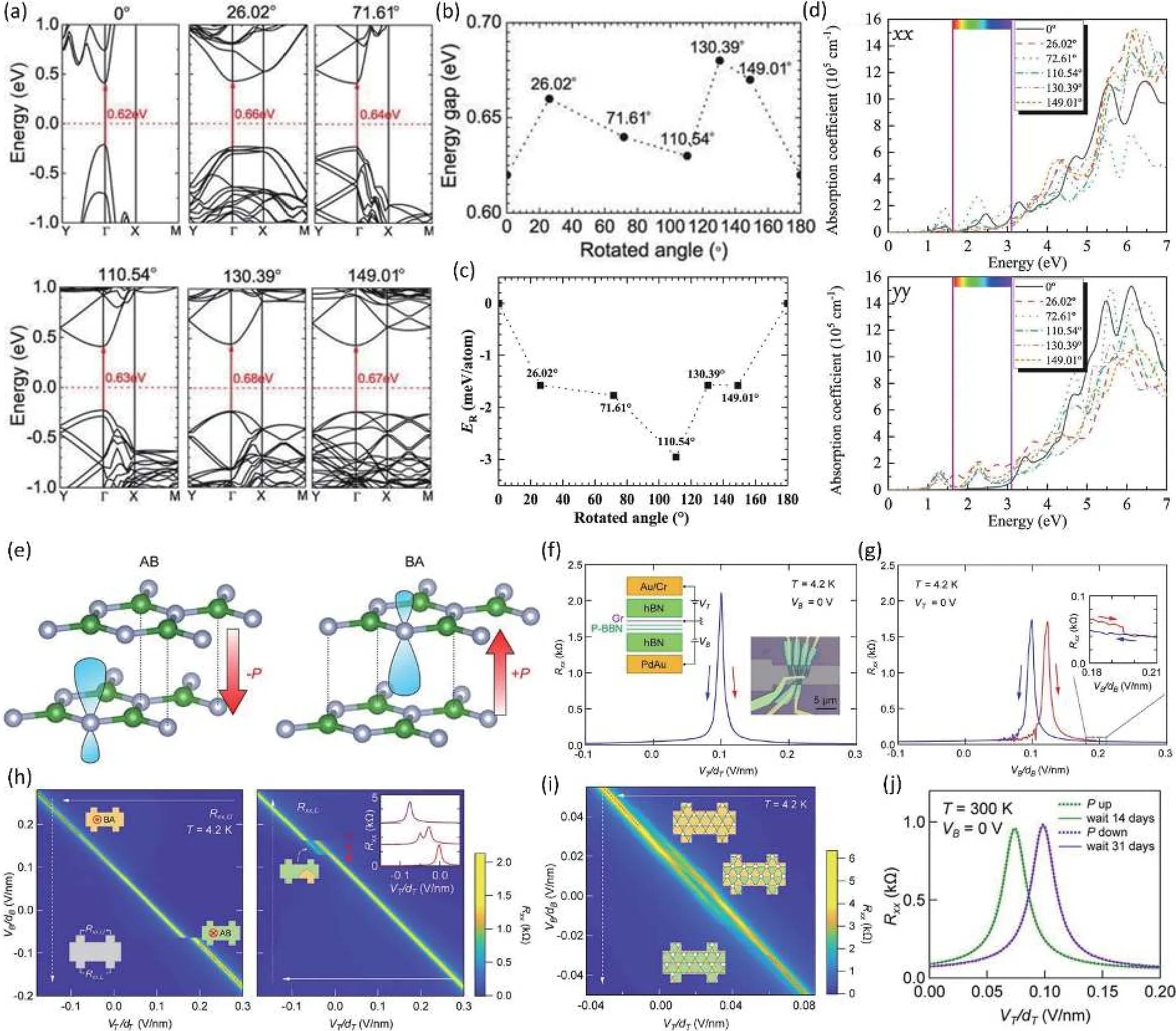
Fig.12.(Color online) (a) Band structure determined by twist-angle of 0°, 26.02°, 71.61°, 110.54°, 130.39° and 149.01° of twisted bilayer black phosphorus (TBBP).(b) Bandgap as a function of twist-angle.(c) Rotated energy defined as the difference between E(θ°) and E(0°) influenced by rotated angle.(d) Absorption coefficient of the bilayer phosphorene with six twist-angles under incident radiation with various energy and different polarization along xx direction (top) and yy direction (bottom).Reproduced with permission[102].Copyright managed by AIP Publishing.(e)Electron cloud of nitrogen atoms (colored gray) induced by orbital hybridization between nitrogen and boron atoms (colored green) and the formation of polarization in AB (left) and BA (right) stacking.(f) The resistance of graphene as a function of the external electric field (VT/dT)where VT and dT is the top gate voltage and the thickness of the top dielectric layer, respectively.Blue and red arrows represent the opposite scanning directions of the top gate voltage.The left inset shows the schematic of the device and the right inset is the optical image of the device.(g)The hysteresis in ferroelectricity of the parallel stacked bilayer h-BN which was reflected by the staggered two peaks of RXX,U during opposite scanning of bottom gate voltage.The inset is the enlarged plot around 0.2 V/nm.(h) The left figure: RXX,U measured through upper contacts (shown in lower left inset) as a function of top and bottom electric field, where the white dashed arrow and solid arrow represents the slow scanning and fast scanning direction, respectively.The higher left inset and lower right inset shows the controllable reversion of polarization.The right figure:RXX,L measured through lower contacts as a function of both two gate electric field.The left inset depicts the pinning of domain wall during the reversion of stacking mode and the right inset describes the relevant resistance peak assigned by the three red arrows on its left.(i) Gradual changing of the stacking mode in Moiré scale (inset schematics), resulting in a gradual reversion of polarization and the resistance detected by graphene rather than abrupt shift in (d).(j) Outstanding stability of polarization after one month at room temperature.Reproduced with permission[75].Copyright 2021, American Association for the Advancement of Science.
4.3.Hexagonal boron nitride
Hexagonal boron nitride (h-BN), which has the same crystal structure as graphene but consists of boron and nitrogen atoms, is a famous and preferable insulator with atomic thickness due to the relatively low covalency between atoms and thus the large bandgap.The analogous 50-fold enhancement of second harmonic generation observed in twisted bilayer h-BN evidenced that h-BN[105], could also be an ideal candidate for dielectric devices based on twisted 2D system.Recently, Yasudaet al.[75]in Pablo Jarillo-Herrero’s research group made twisted bilayer h-BN controllable and stable ferroelectric devices, even though bulk h-BN crystal is a non-ferroelectric compound because of the AA’ stacking.However, owing to energy stability, bilayer h-BN always takes AB or BA stacking in which hybridization between orbitals from nitrogen and boron atoms will lead to the shape distortion of electron cloud in nitrogen and finally induce polarization (Fig.12(e)).In this work, parallel stacked bilayer h-BN and twisted bilayer h-BN with 0.6° were fabricated and formed two Hallbar-like devices compacted with a graphene sensor, two h-BN dielectric layers, and top and bottom gate electrodes,where the bottom gate could affect both the charge carriers in graphene and the electric field across the bilayer h-BN while the top gate could only tune the former one (Fig.12(f)).Therefore, the hysteresis of resistance detected by the graphene sensor in forward and backward scanning by the bottom gate verified the existence of the ferroelectric in the bilayer h-BN system (Fig.12(g)).Once sweeping two gates together, an abrupt shift in resistance was observed, which was attributed to the shift of charge carrier density resulting from the reversal of polarization in bilayer h-BN caused by the external electric field.It was suggested that the polarization reversion in bilayer h-BN from upward (downward) to downward (upward) was realized by the migration of domain walls (Fig.12(h)).Similar interfacial ferroelectricity between the twisted h-BN layers determined by the external electric field was observed by Vizner Sternet al.[106]in the same year, reverifying the electric-field-induced Moiré stacking transformation driven by the reversing of intrinsic charge displacements.
Hence, benefiting from a smaller scale of the Moiré pattern, the twisted bilayer h-BN required smaller coercive electric field than the parallel-stacked bilayer h-BN because not only the migration distance of the domain walls in the former one was much shorter but also the domain wall of the latter one was easy to be pinned by pinning centers, leading to characteristic features in resistance curves of above two cases, respectively (Fig.12(i)).At last, its outstanding stability of polarization at room temperature, shown in Fig.12(j), made it prospective in practical utilization of atomic-thick controllable ferroelectric devices.
In summary, the following Table 2 exhibits primary 2D twist-angle superlattices aforementioned in the article with their twist-angle and several electrical and/or optoelectrical property parameters.From both the number of relevant research papers and the quality of 2D twist-system-based devices, it was suggested that making twist-angle 2D superlattices into (opto)electronic application is still in babyhood.Since twisting needs no heteroatoms introducing which guar-antees the purity and simplicity of the platform, there will be increasing studies on this field, further promoting the development of applications in (opto)electronics.

Table 2.Collection of primary devices and their (opto)electrical property parameters.
5.Conclusion and outlooks
In this article, we elucidated the phylogeny of twist-angle 2D superlattices, especially the feats focusing on the magicangle twisted bilayer graphene.Basically, the novel and intriguing properties of twisted 2D superlattices can be attributed to the twist-angle-dependent electronic structures with the formation of a Moiré pattern.So far, it is generally accepted that the significant enhancement of photoresponsivity in TBG is correlated with the emergence of van Hove singularities in DOS due to the merging of two Dirac cones of top and bottom sheets, while the distinct enhancement of a photoluminescent response in TBTMDs is caused by the recombination of interlayer excitons stemming from the adjustable interlayer coupling.Besides, twist-induced new transition routes and could significantly enhance the matter-light interaction provide the opportunity to promote the applications in optical nonlinearity of twisted 2D systems.
It is notable that there is a so-called magic angle in the twisted bilayer graphene system, at which the Dirac cones around the Fermi level are flattened and the density of states of carriers is localized, resulting in strong correlated states and thus a series of intriguing phenomenon.Combining with the external electrostatic field, MATBG has been made a Josephson junction and a single electron transistor by tuning different regimes into different phases.This inspires later studies on analogous twisted 2D superlattices like TBTMDs which performed similar flat bands and correlated states under certain conditions while the similar honeycomb structure in h-BN certified the possibility for the realization of controllable ferroelectricity through rotational stacking.
Considering the difficulty in fabrication and instability, predicted properties of other twisted 2D systems, such as BP,still lack experimental realization, even though outstanding tunable anisotropy, rectification and polarization-sensitivity have been theoretically proved.Hence, it calls for further investigation on the verification of the intriguing predictions.On the other hand, the development of an optoelectronic device based on TBTMDs are obviously slower than TBG, not only because of the more intricating elemental constituents and crystal structure, but also due to the inefficient band engineering through twisting.Theoretically, however, TBTMDs should possess similar attractive properties and applications as TBG, hence research both on simulation and experiment are required, with the help of understanding the deeper mechanisms for TBG-analogous features in TBTMDs.
We believe more surprising findings are on the way and these outstanding feats on twist-angle 2D superlattices are just a commencement.Owing to the new freedom in tuning the (opto)electronic properties, the twisted 2D systems are expected to become critical candidates for controllable microelectronic and optoelectronic devices.
Acknowledgements
This work was financially supported by the Strategic Priority Research Program of Chinese Academy of Sciences (Grant No.XDB43000000), and the CAS-JSPS Cooperative Research Project (No.GJHZ2021131).
杂志排行
Journal of Semiconductors的其它文章
- High-power InAlAs/InGaAs Schottky barrier photodiodes for analog microwave signal transmission
- A 357.9 nm GaN/AlGaN multiple quantum well ultraviolet laser diode
- All-optical switching based on self-assembled halide perovskite microwires
- Alkali metal cation engineering in organic/inorganic hybrid perovskite solar cells
- F-containing cations improve the performance of perovskite solar cells
- Anisotropic 2D materials for post-Moore photoelectric devices
