Anisotropic 2D materials for post-Moore photoelectric devices
2022-02-15DingdongXieJieJiangandLimingDing
Dingdong Xie, Jie Jiang,†, and Liming Ding
1Hunan Key Laboratory of Super Microstructure and Ultrafast Process, School of Physics and Electronics, Central South University,Changsha 410083, China
2Center for Excellence in Nanoscience (CAS), Key Laboratory of Nanosystem and Hierarchical Fabrication (CAS), National Center for Nanoscience and Technology, Beijing 100190, China
Since the discovery of two-dimensional (2D) graphene[1],2D materials have been widely investigated due to their intriguing physical/chemical property and outstanding optoelectronic performance[1−3].Generally, 2D materials can be divided into isotropy and anisotropy according to crystal structures.For isotropic 2D materials like graphene and hexagonal boron nitride, they have obvious lattice symmetry.Whereas, anisotropic 2D materials possess strong anisotropic crystal structure (Fig.1(a)), providing new degree of freedom for exploring 2D materials.Currently, 2D materials with high anisotropy, due to their anisotropic electrical, optical, thermal, and phonon properties, are finding applications in polarizationsensitive photodetection, neural network construction, spinpolarized transport and other emerging fields[3−6].
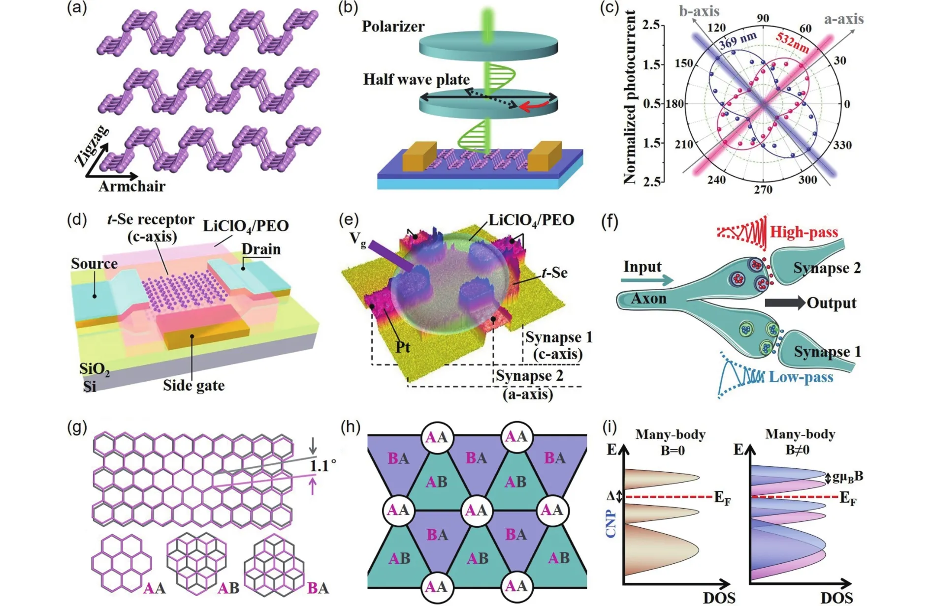
Fig.1.(Color online) (a) Multilayer black phosphorus.(b) Schematic diagram of the polarization-sensitive photodetector based on anisotropic 2D materials.(c) Normalized photocurrents in the polar coordinates.Reproduced with permission[4], Copyright 2020, John Wiley and Sons.(d)Three-terminal EGT to mimic the synapse behavior.Reproduced with permission[9], Copyright 2020, American Chemical Society.(e) The EGT device with a pair of opposite electrodes.Reproduced with permission[9], Copyright 2020, American Chemical Society.(f) Biological axon-multisynapse system.(g) Top: the Moiré pattern in TBG.Bottom: three different stacking in TBG.(h) A simplified model for the stacking order in TBG.(i)Density of states.Left: a spin-singlet Mott-like insulator ground state.Right: the excitations can be polarized and charge conduction occurs when the Zeeman energy exceeds the charge gap.
In layered 2D materials, the in-plane atoms are held together by strong covalent bonds, while different layers are stacked by weak van der Waals (vdW) forces[7].2D materials can be easily exfoliated from layered crystals, and present a large surface-to-volume ratio.Interestingly, anisotropic 2D materials possess excellent polarized photodetection abilities because of their intrinsic sensitivity to polarized light[8].A novel polarization-sensitive photodetector based on anisotropic 2D materials has recently been proposed (Fig.1(b)).In such devices, the laser is set to pass through a polarizer, and then the direction of incident light can be controlled by a halfwave plate.2D anisotropy phototransistor can convert polarization characteristics into electrical signals.Such polarizationsensitive photodetectors will find applications in optical communication, near-field imaging, navigation, and military fields[7−9].
In 2020, Piet al.[4]reported a highly sensitive polarized photodetector based on 2D palladium diselenide (PdSe2).PdSe2not only possesses high room-temperature mobility and high air stability, but also has a puckered pentagonal structure with highly anisotropic properties, which gifts it advantages in polarization detection.The strong anisotropic photoelectric properties of 2D PdSe2were revealed by azimuthdependent reflectance difference microscopy.The polarized photodetector presented excellent performance with dichroic ratios as high as ~2.2 at 369 nm and ~1.8 at 532 nm, respectively (Fig.1(c)).Moreover, their primary polarization orientations differed by 90°, which is due to the characteristic difference betweena-axis andb-axis.This phenomenon was ascribed to the inherent linear dichroism of PdSe2.Very recently, Liet al.[5]also demonstrated that PdSe2photodetector possesses excellent polarization sensitivity and high stability.The phonon anisotropy of PdSe2was confirmed by polarization-dependent Raman.Such polarization-sensitive photoresponse based on photothermoelectric effect was also demonstrated.These results indicate that anisotropic 2D materials can promote the development of next-generation high-performance polarized photodetection systems.
Compared with traditional 2D materials, anisotropic 2D materials like black phosphorus, ReS2, and PdSe2show strong anisotropy in their crystal structure and photoelectric property[4−8].The related devices can offer a high intrinsic heterogeneity for information transmission.In biological synapses,the heterogeneity of synaptic connections is the basis for the diversity of neural activity[6].The realization of heterogeneity in synaptic plasticity is very crucial for constructing high-complexity neural networks.Therefore, the setup based on anisotropic 2D materials can bring intrinsic heterogeneity into new-generation neuromorphic electronics.
Tianet al.[6]realized the first anisotropic neuronal transistor based on black phosphorus.They used structure anisotropy of 2D materials to imitate the heterogeneity of synaptic behavior.The key characteristics of biological synapses were successfully emulated, such as long-term plasticity and spike-timing-dependent plasticity.More importantly, a simple axon-multi-synapse heterogeneity network was demonstrated.These devices can be regarded as the building blocks for future neuromorphic systems.
Recently, Qinet al.[9]used 2D trigonal selenium (t-Se)nanosheet to make an anisotropic electrolyte-gated synaptic transistor (EGT) (Fig.1(d)).t-Se is a one-dimensional vdW material, where Se atoms are covalently bonded alongc-axis direction while stacked together along the perpendicular plane via vdW interactions.2D t-Se nanosheets tend to crystallize in an irregular quadrilateral.In the EGT devices based on t-Se nanosheets, the synaptic weight variation and temporal filtering capability showed a strong anisotropic response because of the inherent heterogeneity of channel conductance.Moreover, the complex axon-multi-synapse system with heterogeneous signal-transmission ability was also realized in multiterminal EGT devices (Fig.1(e)).For the same stimulus input, the system exhibited an anisotropic filtering behavior(Fig.1(f)).The devices based on 2D anisotropic materials can be used to build heterogeneous artificial neural networks.
Some isotropic 2D materials with special structures may have anisotropic functions.A magic-angle graphene has been extensively studied due to its flat-band accessibility,bandwidth tunability, and superconducting phase[10−12].Magic-angle twisted bilayer graphene (TBG) was made by stacking two aligned graphene sheets with a small twist angle ofθ≈ 1.1° (Fig.1(g)).The Moiré pattern can arise from a small twist angle or lattice mismatch between the sheets.A Hubbard model was used to explain the stacking order of TBG(Fig.1(h)), in which each vertex of the trigonal lattice corresponds to A–A stacking of Moiré pattern.When applying a Zeeman field, the excitation can be further polarized.The charge conduction occurs when the charge gap is exceeded by Zeeman energy (Fig.1(i)).Caoet al.[12]recently reported the identification of intertwined phases with rotational symmetry breaking in magic-angle TBG.A highly anisotropic phase was found in a “wedge” above the underdoped position of superconducting dome.This superconducting state exhibited an anisotropic response to a direction-dependent in-plane magnetic field.Both anisotropic 2D materials and isotropic 2D materials with special structures have a great promise in post-Moore photoelectric devices due to their atomic-level thin bodies and unique anisotropic feature.
Acknowledgements
This work is supported by the National Natural Science Foundation of China (52172169) and the Central South University Research Fund for Innovation-driven Program(2019CX024).D.Xie thanks the Fundamental Research Funds for the Central Universities (2020zzts046).L.Ding thanks the National Key Research and Development Program of China(2017YFA0206600) and the National Natural Science Foundation of China (51773045, 21772030, 51922032, 21961160720)for financial support.
杂志排行

Journal of Semiconductors的其它文章
- High-power InAlAs/InGaAs Schottky barrier photodiodes for analog microwave signal transmission
- Twist-angle two-dimensional superlattices and their application in (opto)electronics
- A 357.9 nm GaN/AlGaN multiple quantum well ultraviolet laser diode
- All-optical switching based on self-assembled halide perovskite microwires
- Alkali metal cation engineering in organic/inorganic hybrid perovskite solar cells
- F-containing cations improve the performance of perovskite solar cells