I nvestigation on the passivation, band alignment, gate charge,and mobility degradation of the Ge MOSFET with a GeOx /Al2O3 gate stack by ozone oxidation
2022-02-15LixingZhouJinjuanXiangXiaoleiWangandWenwuWang
Lixing Zhou, Jinjuan Xiang, Xiaolei Wang, and Wenwu Wang
1Faculty of Information Technology, School of Microelectronics, Beijing University of Technology, Beijing 100124, China
2Key Laboratory of Microelectronics Devices & Integrated Technology, Institute of Microelectronics of Chinese Academy of Sciences,Beijing 100029, China
Abstract: Ge has been an alternative channel material for the performance enhancement of complementary metal–oxide–semiconductor (CMOS) technology applications because of its high carrier mobility and superior compatibility with Si CMOS technology.The gate structure plays a key role on the electrical property.In this paper, the property of Ge MOSFET with Al2O3/GeOx/Ge stack by ozone oxidation is reviewed.The GeOx passivation mechanism by ozone oxidation and band alignment of Al2O3/GeOx/Ge stack is described.In addition, the charge distribution in the gate stack and remote Coulomb scattering on carrier mobility is also presented.The surface passivation is mainly attributed to the high oxidation state of Ge.The energy band alignment is well explained by the gap state theory.The charge distribution is quantitatively characterized and it is found that the gate charges make a great degradation on carrier mobility.These investigations help to provide an impressive understanding and a possible instructive method to improve the performance of Ge devices.
Key words: Ge MOSFET; ozone oxidation; gate charges; mobility
1.Introduction
Ge has attracted much attention as a potential channel material with high mobility to replace conventional Si and continue the scaling down of the metal–oxide–semiconductor field effect transistor (MOSFET).In spite of the higher bulk mobility of electron (3900 cm2/(V∙s)) and hole (1900 cm2/(V∙s))than Si[1,2], it still faces obstacles in obtaining superior mobility in practical devices because of the carrier mobility degradation.A high interface quality and optimized gate structure are necessary to boost the Ge MOSFET property.Ge surface passivation has been widely investigated including the nitride passivation layer[3−5], Si cap layer[6,7], and Ge oxide layer[8−10].Among all these surface passivation candidates,GeOxis promising as an interlayer and provides high interface quality.The interface state densityDitis at about 1010–1011cm–2eV–1level[8,10−12].A proper GeOxpassivation layer can be formed by different approaches, such as thermal oxidation[8], plasma treatment[9], and ozone oxidation[10].Leeet al.reported a peak electron mobility of about 1100 cm2/(V∙s)using a 20 nm GeO2layer[13].However, a large equivalent oxide thickness (EOT) with a thick GeOxlayer is not suitable for the requirement of scaled and high-performance devices.When GeOxthickness was reduced at about 1 nm, the apparent increase ofDitwas observed.Zhanget al.has observedDitincrement from 1.7 × 10¹¹to 8 × 1011cm–2eV–1at 0.2 eV below the intrinsic level when GeOxthickness decreased from 1.2 to 0.23 nm for Ge pMOSFET[14].In addition, the hole mobility degraded, with thinner GeOxattributable to the stronger Coulomb scattering fromDit.By plasma post-oxidation, Zhang proposed a structure of HfO2/Al2O3/GeOx/Ge stack with an equivalent oxide thickness (EOT) of 0.7 nm[15].A low interface state density about 1011cm–2eV–1and promoted electron and hole peak mobility value of 754 and 596 cm2/(V∙s) were obtained.
Except for theDiteffect on the mobility degradation, surface roughness scattering[16,17], oxidation atoms in the Ge substrate[18], and remote Coulomb scattering (RCS)[19,20]from the gate stack are also reported to be possible factors causing mobility degradation.The surface roughness characterized by root mean square of the Ge surface has been reduced at 0.11 nm[21].Further promoting the mobility by improving the surface roughness is quite limited.Out-diffusion of oxygen in the Ge substrate by hydrogen annealing is another way to increase the mobility[18].Similar to the effect ofDiton mobility degradation, RCS from the charges in the Ge gate stack also plays an important role on mobility degradation[22−24].For the Si MOSFET, different interface fixed charges were reported in the gate stack[25].Si/interlayer and interlayer/high-kdielectric interface had the fixed charge density estimated to be 1011–1012cm–2level[25−27].The dipole charge density at the SiO2/high-kdielectric interface is experimentally estimated at 1013cm–2level[26,28,29].The mobility suffered severe degradation from the RCS induced by these fixed interface charges and dipole charges[23,26,30,31].The Ge MOSFET has abook=38,ebook=42similar interlayer/highkdielectric gate stack structure.The interface fixed charge and dipole charge possibly exist in the Ge highkgate stack.The positive fixed charge was found at the GeO2/HfO2interface about (2–3) × 1012cm–2in Bellenger’s report[32].Denget al.reported a fixed charge about 4.5 ×1012cm–2at the Ge/GeO2interface and it could be reduced through O2annealing[33].The charge distribution of the Ge high-kstack still needs to be systematically characterized,especially for the dipole charge.
Energy band alignment of highk/Ge stack is a key parameter to affect the electrical characteristics, such as the gate leakage current and interface dipole.Al2O3has been reported to serve as a barrier to restrain the oxygen diffusion and realize a thin GeOxlayer and low EOT[14,21].The Ge MOSFET using the GeOx/Al2O3structure usually showed high performance with enhanced mobility[14,15,21].The band lineup of the Ge/Al2O3and Ge/GeOx/Al2O3stack is discussed in this paper.In addition, the interface passivation, gate charge distribution, and mobility degradation by RCS of the gate charges of Ge/GeOx/Al2O3MOSFET are presented and reviewed from our previous work.The composition of the paper is organized as follows.First, the passivation mechanism based on ozone oxidation is described in Sec.2.The effect of GeOxthickness formed by ozone oxidation onDitis given.It is also a demonstration that whether the changing regular ofDitwith GeOxthickness is the oxidation method related or a common feature regardless of the oxidation method.Second, the band alignment of the Al2O3/Ge stack with different Al2O3or GeOxinterlayer thickness is discussed in Sec.3.Third, the charge distribution in the Al2O3/GeOx/Ge gate stack is characterized in Sec.4.It is found that an interface fixed charge of about 1012cm–2exists as well as an interface dipole charge about 1013cm–2in the gate stack.The mobility degradation induced by the remote Coulomb scattering from the gate charges is discussed in Sec.5.Sec.6 is the part of the conclusion.
2.Ozone passivation mechanism
Obtaining a superior interface is a precondition to realizing a high-performance Ge MOSFET.The dependence ofDiton GeOxthickness was experimentally found both in post thermal oxidation and plasma oxidation.Kuzumet al.reported a suitable temperature control was beneficial to reduceDitbecause of an increase of the Ge4+composition oxidation state[10].We discussed the passivation mechanism of GeOxbased on ozone oxidation, and clarified whether it had a similar dependence relationship ofDiton GeOxthickness compared with thermal or plasma oxidation.
An attracting feature of ozone oxidation is that GeOxcan grow at low temperature which effectively avoids GeOxdesorption (>420 °C)[34,35].Fig.1(a) shows the relationship between GeOxthickness and oxidation time for different deposition temperature.The temperature of ozone oxidation varied from 80 to 400 °C.The GeOxthickness is about 2.8, 5.28, 7.8,9.7, and 12.3 Å after 25 min ozone oxidation at 80, 250, 300,350, and 400 °C, respectively.The GeOxgrowth presents two different trends with initial linear and subsequent parabolic mode.The GeOxgrowth phenomenon observed here is similar to Si oxidation interpreted by the Deal-Grove mode[36].The GeOxgrowth in the linear region is supposed to be determined by reaction rate at the Ge/GeOxinterface.While it is limited by diffusion rate of oxygen through GeOxin the parabolic region.Fig.1(b) shows the Arrhenius plot for the linear and parabolic region.The activation energy in the linear growth is calculated to be 0.06 eV, which is nearly consistent with that of Si oxidation[37−39].Such small activation energy of Ge oxidation indicates a nearly barrier-less growth for the initial oxidation stage.The activation energy in the parabolic region is estimated to be 0.54 eV.Compared with thermal oxidation, the activation energy is much smaller in ozone oxidation which may have a higher reactivity of oxygen atoms to create the Ge–O–Ge bond.
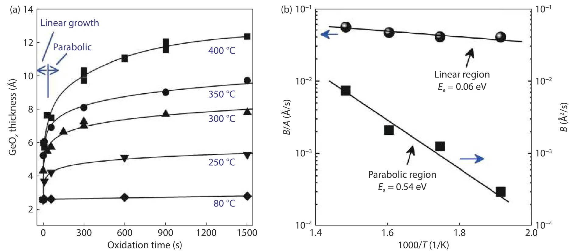
Fig.1.(a) GeOx thickness with oxidation time at temperature varying from 80 to 400 °C.(b) Arrhenius plots for linear and parabolic region.Ea is activation energy.
book=39,ebook=43
The electrical property of the Ge/GeOx/Al2O3gate stack by ozone oxidation is presented in Fig.2.Fig.2(a) shows the capacitance–voltage (C–V) property of W/TiN/Al2O3/GeOx/Ge MOS capacitor with 1.06 nm GeOx.Well-shapedC–Vcurves reflect a good Ge/GeOxinterface.Ditis measured by the conduction method at low temperature and drew in Fig.2(b).Fig.2(b) shows theDitapparently decreases with GeOxthickness increasing.The inset of Fig.2(b) is the energy distribution ofDitwith different thicknesses of the GeOxlayer.When GeOxthickness is larger than 0.6 nm,Ditis nearly unchanged and reaches a minimum saturation value of about 3 ×1011cm–2eV–1.This result demonstrates that a GeOxthickness larger than 0.6 nm is necessary to ensure good passivation quality.Compared with thermal or plasma oxidation,ozone oxidation also induces the sameDitdependence trend on GeOxthickness.Therefore, the surface passivation of Ge using GeOxseems to have the same mechanism regardless of the oxidation method.
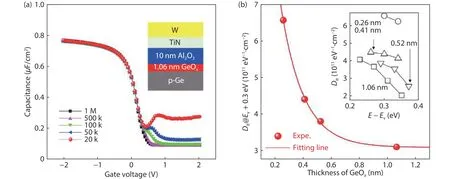
Fig.2.(Color online) (a) Capacitance–voltage curves of W/TiN/Al2O3/GeOx/Ge capacitor.(b) Dit values at 0.3 eV above Ev for different GeOx thickness and the inset shows the Dit energy distribution of W/TiN/Al2O3/GeOx/Ge capacitors with different GeOx thickness.
To understand the behavior ofDitdecreasing with an increasing GeOxthickness, the oxidation state of Ge is analyzed by X-ray photoelectron spectroscopy (XPS) technology.Fig.3 shows the XPS spectra of Ge 3d for GeOx/Ge for different GeOxthickness.In order to quantitatively evaluate each oxidation state of the Ge, the Ge 3d spectra are divided by five peaks related to the Ge substrate (Ge0), Ge suboxide (Ge1+,Ge2+, Ge3+) and GeO2(Ge4+) components.The chemical shifts of Ge1+, Ge2+, Ge3+and Ge4+relative to the Ge0are taken as 0.8, 1.8, 2.75 and 3.4 eV, respectively[40−43].It can be seen that the peak corresponding to the GeOxincreases with thicker GeOx, and the GeOxpeak energy shifts toward higher binding energy, suggesting that the oxidation state of Ge and the GeOx/Ge interfacial structure are dependent on the GeOxthickness.
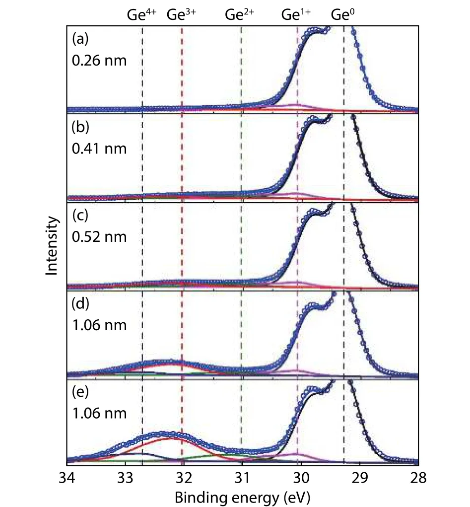
Fig.3.(Color online) XPS spectra of Ge 3d for GeOx/Ge for different GeOx thickness.The takeoff angel in (a)–(d) is 90° (normal to the sample surface) and it is 35° in (e).
The peak area intensity ratio of Ge1+, Ge2+, Ge3+, and Ge4+component to Ge0component as a function of GeOxthickness is shown in Fig.4(a).The Ge1+component has an extremely small change with GeOxthickness.The Ge2+component has a slight increase when GeOxthickness is below 0.4 nm.While it is nearly unchanged when GeOxthickness is larger than 0.4 nm.It can be seen from Fig.2(b) thatDitstill obviously decreases for GeOxthickness above 0.4 nm.At the same time, the Ge4+component is not detected for the GeOxthickness of less than 0.52 nm.The Ge3+component shows a monotonical increase with increasing GeOxthickness.Therefore, Ge1+, Ge2+, and Ge4+components are less relevant withDitpassivation.The Ge3+component increment with GeOxthickness plays a main role on passivatingDit.Fig.4(b) shows the area intensity ratio values of Ge2+/Ge1+, Ge3+/Ge1+,Ge4+/Ge1+, and Ge3+/Ge2+as a function of takeoff angle for 1.06 nm GeOx.The values of Ge2+/Ge1+, Ge3+/Ge1+and Ge4+/Ge1+decrease with an increased takeoff angle.It reflects the Ge2+, Ge3+, and Ge4+components are located in the upper of Ge1+.The value of Ge3+/Ge2+shows no variation when the takeoff angle changes from 35° to 90°, which means that the Ge3+and Ge2+are uniformly mixed.From the above discussion, it can be concluded that a suboxide of Ge composed of Ge1+, Ge2+, and Ge3+is formed.The Ge3+component is beneficial to passivate the Ge surface and decreaseDit.

Fig.4.(Color online) (a) The trend of area intensity ratio of Ge1+, Ge2+, Ge3+, and Ge4+ to Ge0 with different GeOx thickness.(b) The area intensity ratio of Ge2+/Ge1+, Ge3+/Ge1+, Ge4+/Ge1+ and Ge3+/Ge2+ at the takeoff angle of 35° and 90°.
3.Band alignment of Ge/Al2O3 stack
book=40,ebook=44
Energy band alignment at the hetero-interface has always been an attractive and intensive topic in semiconductor science and industry.To improve the injection current and further scale the supply voltage, the highk/Ge stack is very advantageous and preferable[44].One of the key parameters is the energy band alignment which is related with the gate leakage current and interfacial effect such as dipole and charges[45,46].The valence band offset (VBO) has been found to be inconsistent among different research experiments and varied in the range of 3.17–3.4 eV[47−49].The photoemission spectroscopy method measures the signals a few nanometers underneath the surface due to the exponential attenuation of photoelectrons and thus the obtained spectrum is a weighted average of the detected signals but not the signal just on the surface[50].Therefore, the peak position will be affected by the electric potential distribution across the Al2O3/Ge stack induced by surface or bulk charges.In addition, the influence of an interlayer on band alignment has been investigated at the hetero-junction such as HfO2/Si,HfO2/Ge, HfO2/GaN, and TiO2/Si etc.[51−54].For the Al2O3/Ge stack, the effect of the Al2O3and interlayer GeOxthickness on the band alignment is described by the XPS measurement technique.
3.1.Effect of Al2O3 thickness on band offset
The VBO at the Al2O3/Ge interface is described using the method proposed by Krautet al.[55].The expression of VBO is shown as follows,
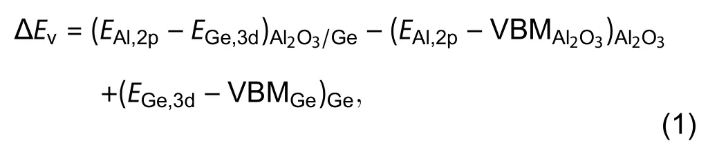
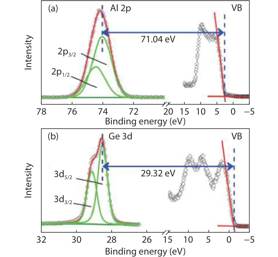
Fig.5.(Color online) The XPS measurements of the valence band and core-level spectra of (a) bulk Al2O3 and (b) Ge substrate.
The XPS measurements of core-level spectra for different Al2O3thicknesses are given in Fig.6.To compare the difference of binding energy between Ge 3d and Al 2p, the peak position of Ge 3d core-level spectra is fixed at the same binding energy.It can be seen that the Al 2p to Ge 3d separation gradually increases with larger Al2O3thickness.The VBO at Al2O3/Ge interface can be calculated based on Eq.(1).Fig.7 shows the dependence of VBO on Al2O3thickness.The measured band offset at the Al2O3/Ge interface increases with Al2O3thickness increasing.It indicates that the electrostatic potential exists across the Al2O3film and induces energy band bending.The core level spectrum, which is the weighted average of the detected photoemission, reflects the potential at a position displaced away from the center of the film toward the outer surface.
book=41,ebook=45

Fig.6.(Color online) The XPS measurements of core-level spectra for different Al2O3 thickness: (a) 2 nm, (b) 4 nm, and (c) 6 nm.
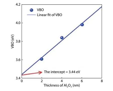
Fig.7.(Color online) The dependence of VBO of the Al2O3/Ge interface on Al2O3 thickness.
The gap state model is widely accepted to explain the physical nature of band alignment at the heterojunction[56−58].When the charge neutrality level (CNL) of the gap states in two adjacent materials is not consistent, electrons then flow from one material with higher CNL to the other with lower CNL.An electric dipole forms to align their Fermi level during the process.The effect of surface gap states on the Al2O3surface is considered to interpret the phenomenon of VBO changing with Al2O3thickness.Due to the hetero-structure at the air/Al2O3interface, the solutions of Schrödinger's equation with complex wave vectors become of physical relevance for energies within band gaps, resulting in gap states on the Al2O3surface.CNL is a defined energy level at which the characteristics of these gap states change from predominately donor- to acceptor-like closer to the valence band top and the conduction band bottom, respectively.
Fig.8 is the schematic of the energy band before and after Al2O3and Ge contact.G SAlOmeans the gap states at the Al2O3surface, and CNLs is the CNL of Al2O3.CNL1means the CNL at the Al2O3/Ge surface (G SAlO/Ge).We assume the CNLs is higher than CNL1before Al2O3and Ge contact as shown in Fig.8(a).Then electrons transfer from the G SAlOto GSAlO/Ge.Negative charges accumulate at the Al2O3/Ge surface and equal positive charges at the Al2O3surface.Fig.8(b)is the energy band diagram after Al2O3and Ge contact.Electron transfer leads to the alignment of Fermi level and band bending across the Al2O3film and at the Ge surface.Because of more influent electron to fill in the G SAlO/Ge, CNL1is not consistent with the Fermi level anymore and shows a downward shift.Similarly, due to the effluent electron from G SAlO,CNLs shows an upward shift compared with the Fermi level.Δ1andΔsrepresent the deviation values of CNL1and CNLs relative to the Fermi level, respectively.ΔBrepresents the potential drop across Al2O3.The difference between CNL1and CNLsis equal to the sum ofΔ1,Δs, andΔB.Δ1andΔsare affected by the number of transferred electrons.With an increasing Al2O3thickness, the number of transferred electrons decreases.So does theΔ1andΔs.The binding energy difference between the Al 2p near the surface and Ge 3d is equal to the sum ofΔs, andΔB, which is also equivalent to the difference between CNL1and CNLs subtractingΔ1.Δ1becomes smaller with increasing Al2O3thickness.Then the binding energy difference increases with thicker Al2O3as shown in Fig.7.The surface state model is well employed to explain the experimentally observed dependence of VBO at the Al2O3/Ge interface on Al2O3thickness.The VBO just at the Al2O3/Ge interface is obtained to be 3.44 eV by the extrapolation method.

Fig.8.The energy band sketch of Al2O3/Ge structure (a) before and (b)after contact.
3.2.Effect of GeOx thickness on band offset
The gap states model was also validated by inserting an interlayer at the hetero-junction.The different thickness GeOxis introduced to investigate the band alignment at the Al2O3/Ge interface.Al2O3thickness remain at 2 nm.GeOxthickness varied from 0.2 to 1.2 nm.Fig.9 shows the dependence of VBO at the Al2O3/Ge interface on the GeOxthickness.It is found that the VBO is unacted on GeOxthickness.As discussed in Sec.3.1, the band alignment at the Ge/Al2O3interface is driven by a matching of CNL at the adjacent materials.When introducing an interlayer, it modifies the matching of CNL by a Schottky barrier pining parametersS[59−61], which is related with the thickness, relative permittivity of GeOxand theDit.For a GeOxinterlayer with thickness of 0.2–1.2 nm,the calculated result just coincides with the experimental data as shown in Fig.9.The VBO is not affected by GeOxthickness.The gap states model is successfully employed to explain the band alignment.

Fig.9.The dependence of VBO of Al2O3/Ge structure on interlayer GeOx thickness.
4.Interface charge in Ge/GeOx/Al2O3 gate stack
4.1.Charge distribution in gate stack
book=42,ebook=46
The interfacial charges in the gate stack is one of the critical issues to enhance the performance of the Ge MOSFET.These charges significantly degrade the electrical characteristics such as threshold voltage shifts[62], reliability[63], and mobility degradation[14,17].Although the high electron and hole bulk mobility, the mobility of the Ge MOSFET still suffers severe degradation.The remote Coulomb scattering from gate charge plays a key role on mobility degradation.Therefore, it is very instructive to quantitatively characterize the charge distribution in the gate stack of Ge MOSFET.The charge distribution is obtained by employing the relationship between flatband voltage (VFB) and EOT.TheVFBand EOT relationship is measured through a Ge/GeOx/Al2O3capacitor combining different GeOxand Al2O3thickness as shown in Fig.10.Figs.10(a) and 10(b) show theVFBand EOT relationship for capacitors with varied GeOxand Al2O3thickness, respectively.The theoretic expression for structure in Fig.10(a)is shown as

Fig.10.(Color online) The relationship of VFB and EOT of Al/Al2O3/GeOx/Ge capacitors with different (a) GeOx and (b) Al2O3 thickness.
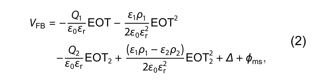
whereQ1is the areal charge at the Ge/GeOxinterface,Q2is the areal charge at the GeOx/Al2O3interface,ρ1is bulk charge density in GeOx,ρ2is bulk charge density in Al2O3,ε0is the vacuum permittivity,εris the relative permittivity of SiO2,ε1is the relative permittivity of GeOx,ε2is the relative permittivity of Al2O3, EOT is the equivalent oxide thickness of the whole gate stacks, EOT2is the equivalent oxide thickness of the Al2O3dielectric,ΔmeansVFBshift due to the electric dipole at the GeOx/Al2O3interface, andϕmsis the vacuum work function difference between the Al gate electrode and Ge substrate.
The theoretic expression for structure in Fig.10(b) is shown as
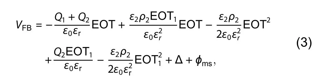
where EOT1is the equivalent oxide thickness of the GeOxdielectric.The linear fitting is obtained, as shown in Figs.10(a) and 10(b).Then the fixed chargesQ1at the Ge/GeOxinterface, fixed chargesQ2at the GeOx/Al2O3interface and dipole charge at the GeOx/Al2O3interface can be extracted from the fitting line combining the Eqs.(2) and (3).The space distribution of the interface fixed charge and dipole is shown in Fig.11(a).Fig.11(b) gives the charge density of these charges.The fixed chargeQ1at the Ge/GeOxinterface, fixed chargeQ2at the GeOx/Al2O3interface, dipole at the GeOx/Al2O3interface are estimated to be 7 × 10¹², –3.06 ×10¹², and 1.98 × 1013cm–2, respectively.The density of the dipole charge is larger than the fixed charge.
book=43,ebook=47
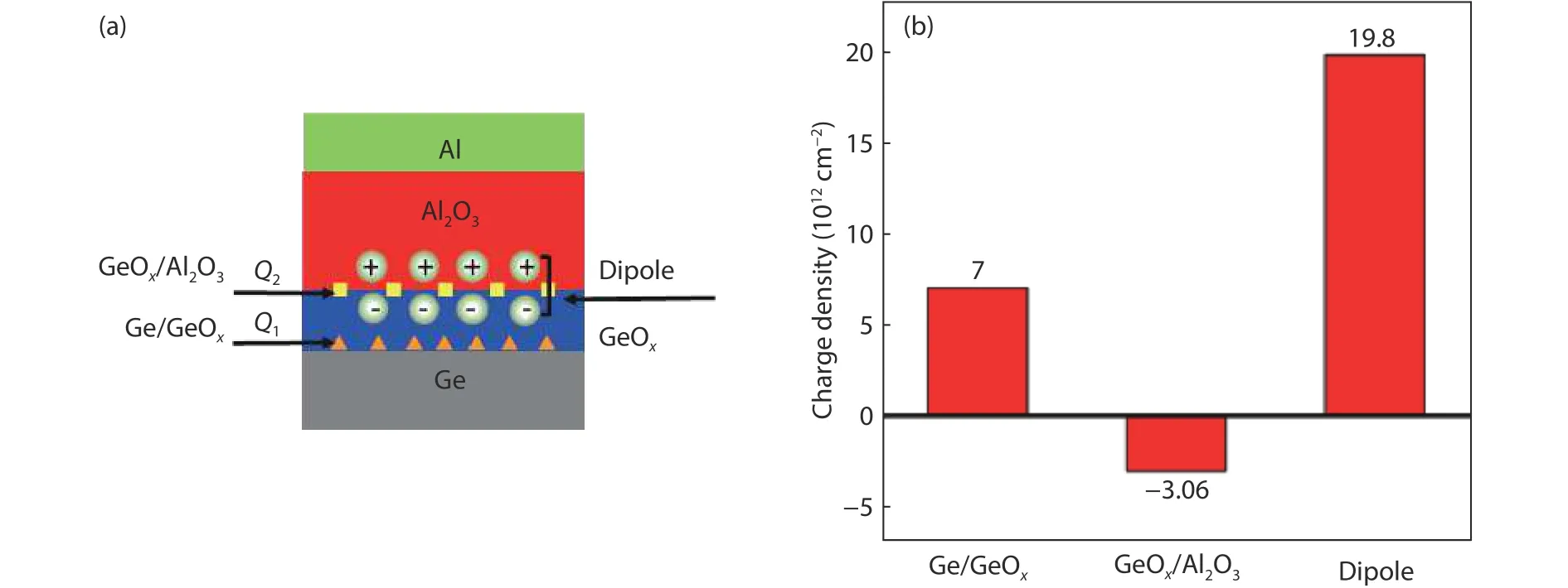
Fig.11.(Color online) (a) The charge distribution and (b) the charge density in the Al/Al2O3/GeOx/Ge structure.
4.2.Origin of gate charge
To effectively modulate the charge distribution in the gate stack, understanding the origin of interface fixed charge and dipole remains a necessity.As discussed in Sec.2, the Ge suboxide is formed at the initial stage of ozone oxidation.The Ge4+oxidation state is not detected when the GeOxthickness is less than 0.52 nm.In other words, the Ge surface is not sufficiently oxidized.In addition, we investigated the areal intensity ration of Ge and O atom in different thicknesses of GeOx.The experimental result shows that the ratio of Ge/O decreases in a thicker GeOx.It also demonstrates that oxygen is relatively deficient at the beginning of ozone oxidation and results in Ge2O formation at the Ge/GeOxinterface.Oxygen deficiency results in oxygen vacancy at the Ge/GeOxinterface.To confirm the oxygen vacancy, post-deposition annealing in oxygen atmosphere is used to investigate the interface property.Fig.12(a) compares theVFBand EOT relationship for Ge/GeOx/Al2O3capacitors with and without O2annealing.The annealing temperature is 400 °C to avoid the GeOxdecomposition.The slope of theVFB–EOT fitting line after O2annealing is smaller than that without O2annealing.The slope described as Eq.(1) represents the charge density at the Ge/GeOxinterface.The specific charge density at Ge/GeOxinterface extracted is shown as Fig.12(b).The positive charge density at Ge/GeOxinterface is 7.34 × 10¹²and 2.37 × 1012cm–2for the as-grown and O2-annealed samples, respectively.O2annealing significantly decreases the fixed charge density at the Ge/GeOxinterface.Extra oxygen is introduced to passivate the oxygen vacancy during the O2PDA.
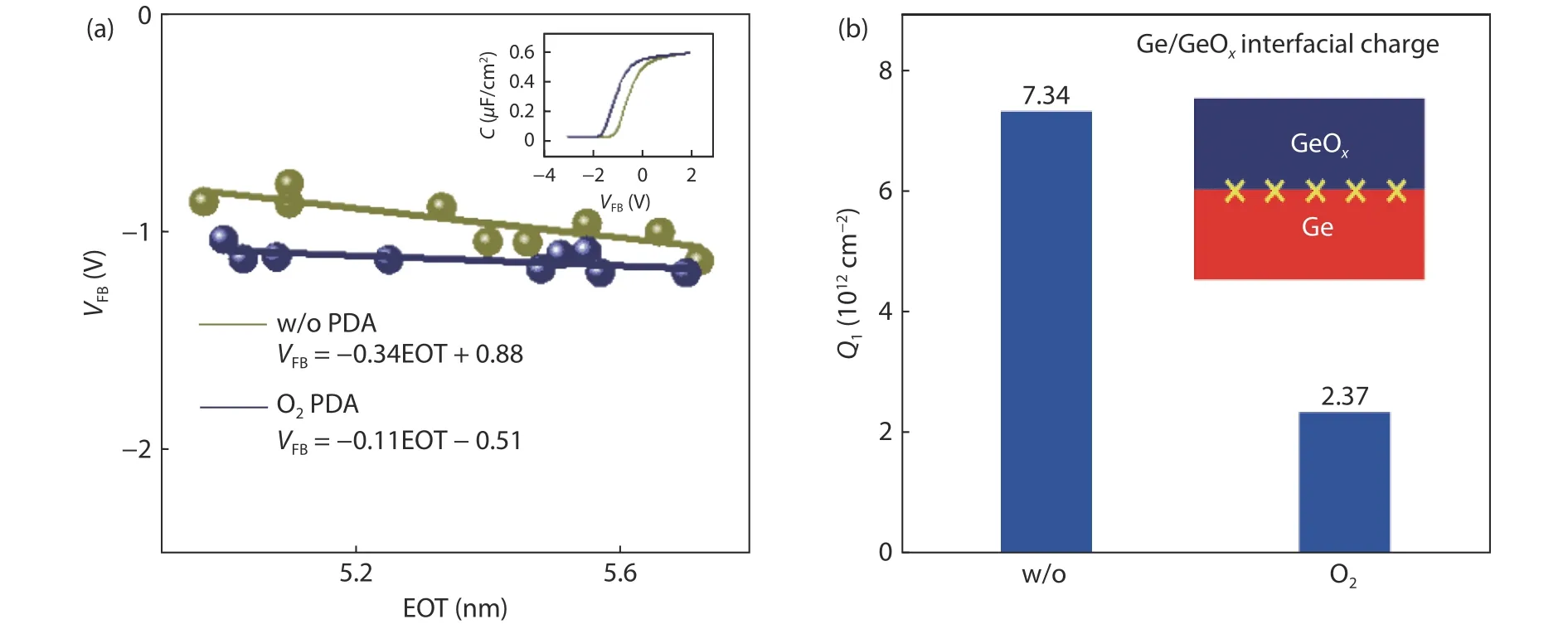
Fig.12.(Color online) (a) The relationship of VFB and EOT and (b) charge density at Ge/GeOx interface of Al/Al2O3/GeOx/Ge capacitors with and without O2 annealing.
As for the origin of fixed charges at the GeOx/Al2O3interface, the property of Al2O3with different thickness is investigated by XPS measurement.Fig.13 gives the intensity ratio of rge aluminum to oxygen for different thicknesses of Al2O3.An increasing ratio of aluminum to oxygen content is obtained with Al2O3thickness increasing.This means aluminum is relatively deficient at the initial stage of Al2O3deposition and an oxygen-rich area exists at the GeOx/Al2O3interface.The high oxygen content results in oxygen dangling bond at the GeOx/Al2O3interface.Based on a first-principles calculation,the transition level of oxygen dangling bonds is located at 0.9 eV above the valence band maximum (VBM) of Al2O3[64].The VBO between Ge and Al2O3was reported about 3.1–3.4 eV[47,48,65].The transition level of oxygen dangling bond is localized below Ge VBM and negatively charged.This is consistent with the experimental result of negative charge extracted at the GeOx/Al2O3interface.Therefore, it is rational to conclude that the oxygen dangling bond results in the negative charge at the GeOx/Al2O3interface.
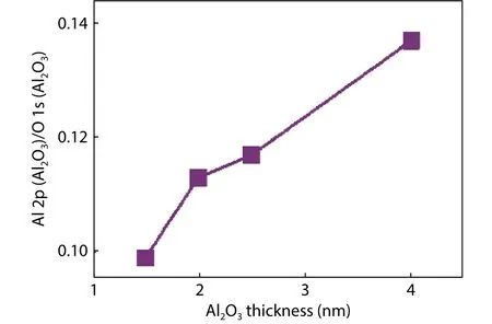
Fig.13.The area intensity ratio of Al 2p to O 1s in Al2O3 with different Al2O3 thickness.
The dangling bond can be passivated by combining other atoms and removing the transition level from the energy gap.It has been observed that oxygen annealing can passivate the oxygen vacancy or Ge dangling bond and decrease the fixed charge density at the Ge/GeOxinterface.To investigate the change of fixed charge at Ge/GeOxand GeOx/Al2O3interface, N2, O2, NH3and H2ambients are used to anneal the Ge/GeOx/Al2O3capacitor samples.Figs.14(a) and 14(b) show fixed charge density at the Ge/GeOxand GeOx/Al2O3interface for the samples without and with PDA in N2, O2, NH3,and H2ambient.It can be seen that the fixed charges at the Ge/GeOxand GeOx/Al2O3interfaces can be obviously changed by PDA in different ambients.Both the quantity and polarity of these interfacial charges can be modulated.O2and NH3PDA is beneficial to suppress the interfacial charges.Figs.14(c) and 14(d) are dipole distribution and correspond-book=44,ebook=48ing areal charge density of dipole at the GeOx/Al2O3interface for the samples with and without PDA.The results show that a positive dipole is obtained only for the as-grown sample.The polarity of the dipole changes to negative after PDA.
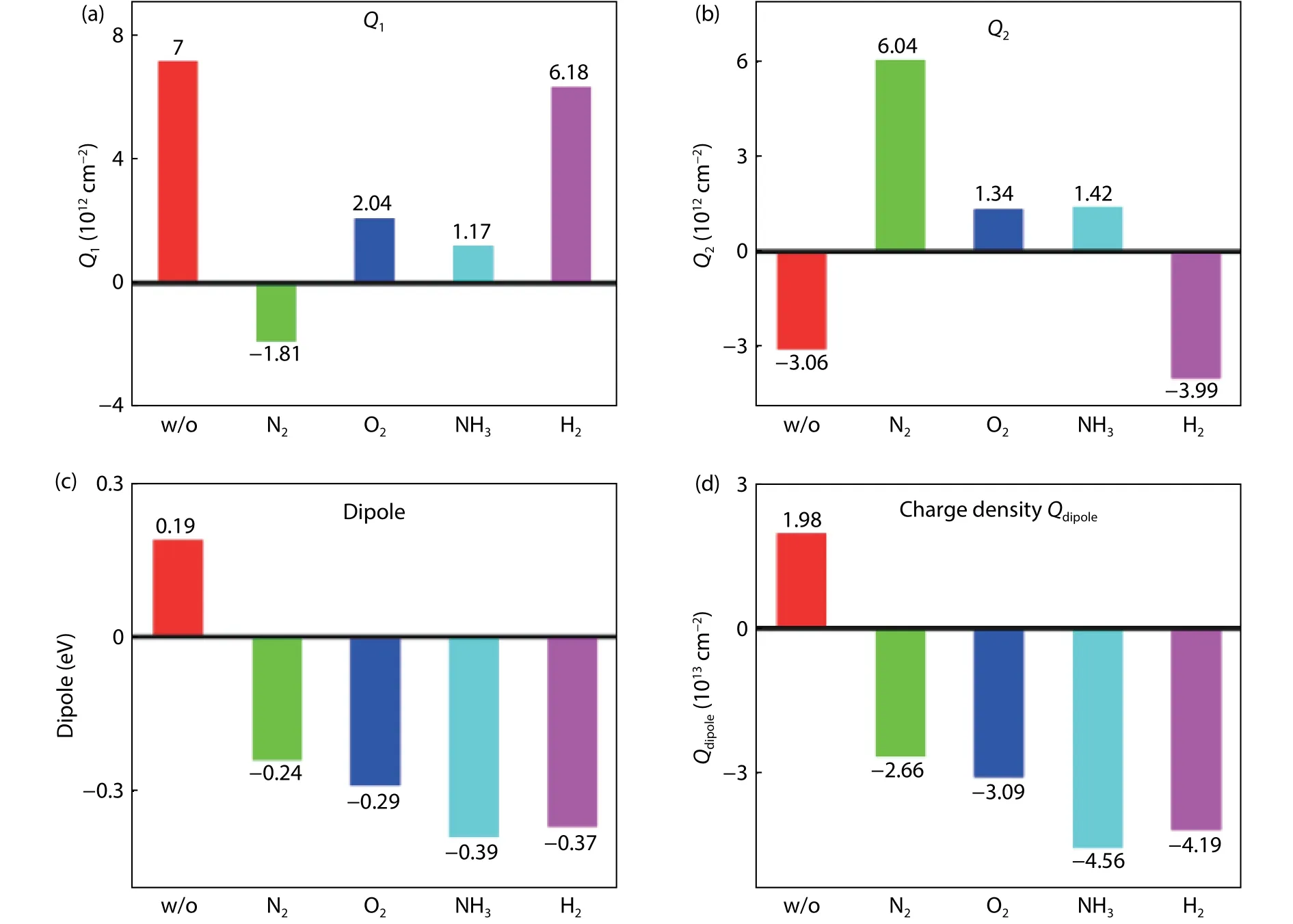
Fig.14.(Color online) The charge density at (a) the Ge/GeOx and (b) GeOx/Al2O3 interface for different ambient annealing.(c) and (d) are dipole and corresponding charge density at the GeOx/Al2O3 interface for different ambient annealing.
To understand the change origin of dipole after different ambient PDA, the XPS measurement was employed to analyse the band structure of the Ge/GeOx/Al2O3stack.Fig.15 depicts the Ge 3d and Al 2p spectra for the Ge/GeOx/Al2O3structure with and without PDA.Ge 3d has two peak positions:the higher peak position from Ge substrate is located at 29.6 eV, and the other from GeOxis near 32.6 eV.The energy scale is calibrated by setting the binding energy of the Ge substrate to be 29.6 eV.The peak position of Ge 3d from GeOxand Al 2p from Al2O3shows a left shift for the samples after PDA in N2, O2, H2, and NH3ambients.The shift extent gradually increases for the N2, O2, H2, and NH3PDA.We have observed a positive dipole for the sample without PDA and an increasing negative dipole in N2, O2, H2, and NH3PDA.The XPS measurement result and electrical dipole extraction are very consistent.Because of the dipole at the GeOx/Al2O3interface,it will lead to the band bending of GeOxand Al2O3at the interface and a shift of core level of GeOxand Al2O3.
Fig.16 is the energy structure of Ge/GeOx/Al2O3stack without a dipole, with a positive, and with a negative dipole at the GeOx/Al2O3interface.δ(G e 3dGeOx– Ge3dGesub) andδ(A l 2pAlO– G e 3dGesub) mean the distance between Ge 3d in GeOxand Ge 3d in Ge substrate and distance between Al 2p in Al2O3and Ge 3d in the Ge substrate, respectively.When no dipole is present at the GeOx/Al2O3interface, the energy band is flat.If a positive dipole at the GeOx/Al2O3interface exists, it decreases the energy band of Al2O3andδ(A l 2pAlO–Ge 3dGesub) becomes larger.At the same time, the energy band bends downward for GeOxand upward for Al2O3at the GeOx/Al2O3interface.Therefore, the value ofδ(G e 3dGeOx–Ge 3dGesub) also becomes larger.While for the negative dipole at the GeOx/Al2O3interface, the energy band level of Al2O3increases.At the same time, the energy band bends upward for GeOxand downward for Al2O3at the GeOx/Al2O3interface.The value ofδ(G e 3dGeOx– G e 3dGesub) andδ(A l 2pAlO–book=45,ebook=49Ge 3dGesub) decrease.Moreover, the value ofδ(G e 3dGeOx–Ge 3dGesub) andδ(A l 2pAlO– G e 3dGesub) becomes smaller when the dipole at the GeOx/Al2O3interface is larger.Namely, the core level peak of Ge 3d in GeOxand Al 2p in Al2O3shift left more severely as shown in Fig.15.
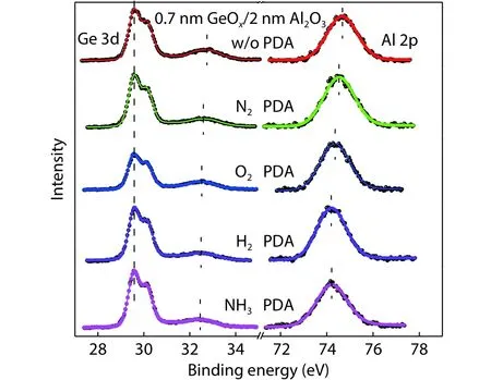
Fig.15.(Color online) The core level spectra of Ge 3d and Al 2p of Ge/GeOx/Al2O3 structure without PDA and with PDA in N2, O2, H2, and NH3 ambients.

Fig.16.The energy band schematic of the Ge/GeOx/Al2O3 structure (a) without dipole, (b) with a positive dipole, and (c) negative dipole at the GeOx/Al2O3 interface.
The CNL theory is still valid to explain the origin of the positive and negative dipole at the GeOx/Al2O3interface.The CNL plays a similar role to the Fermi level.If the CNL in two adjacent materials is not consistent, the electron will transfer from one material with higher CNL to the other and it induces an electrical dipole at the interface.The positive dipole is obtained at the GeOx/Al2O3interface for the sample without PDA.It means CNL in Al2O3is higher than that in GeOx.Electron flows from Al2O3to GeOx, causing negative charge accumulating on the GeOxside and equal positive charge on the Al2O3side.Therefore, a positive dipole forms at the GeOx/Al2O3interface.The negative dipole is obtained at the GeOx/Al2O3interface after PDA, indicating the CNL in Al2O3is lower than that in GeOx.Electron transfers from GeOxto Al2O3, which induces a negative dipole at the GeOx/Al2O3interface.The larger the CNL difference between Al2O3and GeOx, the more electrons will transfer and induce more dipole density.Therefore, the core level of Ge 3d and Al 2p shifts more with a larger dipole.
5.Remote Coulomb scattering of gate charge
We have analyzed the charge distribution in the gate stack in Sec.3.The effect of gate charges on mobility property is discussed in the following content.Fig.17 gives theId–Vgcharacteristics and hole mobility of the Ge pMOSFET with different GeOxthickness by ozone oxidation measured at 77 K.It can be seen thatIdand mobility decrease when the GeOxthickness is thinner.This phenomenon of mobility degradation will be discussed from the viewpoint of the scattering mechanism mainly including the Coulomb scattering,phonon scattering and surface roughness scattering.The root mean square (RMS) is experimentally determined to be identical (~0.09 nm) for different GeOxthickness[20].In addition, the mobility is measured at the same temperature of 77 K.The phonon scattering is sufficiently suppressed and can be ignored.Therefore, the surface roughness scattering and phonon scattering are excluded to induce the mobility degradation for a thinner GeOx.The Coulomb scattering is explored to explain the mobility dependence on GeOxthickness.

Fig.17.(Color online) (a) Id–Vg curves and (b) hole mobility versus inversion carrier density of Ge pMOSFET with different GeOx thickness measured at 77 K.
In Sec.3, we have discussed the distribution of gate charges.There are three kinds of charges in the Ge/GeOx/Al2O3gate stack, including Ge/GeOxinterface chargeQ1, GeOx/Al2O3interface chargeQ2, and interface dipole.It is found that the dipole charge at the GeOx/Al2O3interface is one order of magnitude larger than the fixed charge at the Ge/GeOxand GeOx/Al2O3interface.Fig.17 shows the mobility decreases with the GeOxthickness decreasing.The fixed charge at the Ge/GeOxinterface has the same effect on mobility of the Ge pMOSFET with different GeOxthickness.The mobility degradation is from the charges at the GeOx/Al2O3interface.The Coulomb scattering from the fixed charge and the dipole at the GeOx/Al2O3interface increases with GeOxthickness decline and induces mobility degradation.The charge density of the dipole is higher than the fixed charge at the GeOx/Al2O3interface.Therefore, the remote dipole scatteringbook=46,ebook=50plays a main role in mobility degradation dependent on the GeOxthickness.
The gate charges can be modulated in different PDA ambients.To further certify the Coulomb scattering from the gate charge, the hole mobility extracted from Ge pMOSFET in different PDA ambients is shown in Fig.18.The hole mobility shows obvious variation among different PDA ambients.N2ambient increases the hole mobility, while the NH3and H2ambients decrease the hole mobility compared to mobility without PDA.The substrate material, gate stack structure,and measurement temperature for different PDA samples are all the same as those used in this study.In addition, the highresolution transmission electron microscope (HRTEM) images shows no changes at the interface and film thickness[66].Therefore, the phonon scattering and surface roughness is excluded to affect the mobility at different PDA ambients.The Coulomb scattering is responsible for the mobility variation after PDA.Dithas been extracted and demonstrated not to be affected by different PDA ambients.All the samples have almost the same interface quality andDit[66].So, the hole mobility affected byDitis also excluded.The reason for mobility changes now points to the interface charge and dipole modulated by PDA.

Fig.18.(Color online) Hole mobility versus inversion carrier density of Ge pMOSFET for different PDA ambients measured at 300 K.
First, the Ge/GeOxinterfaceQ1is sufficiently decreased in N2, O2, and NH3PDA shown as in Fig.14(a).The Coulomb scattering fromQ1is greatly decreased.However, the mobility only shows an increase in N2ambient.NH3and O2PDA decrease the hole mobility.It demonstrates that there are other charges in the gate stack degrading the mobility more severely than the Ge/GeOxinterface chargeQ1in NH3and O2PDA.Second, we consider the fixed charges and dipole at the GeOx/Al2O3interface.The GeOx/Al2O3interface chargeQ2is significantly decreased but still does not help in enhancing the hole mobility in O2and NH3ambients.In contrast, the dipole at the GeOx/Al2O3interface increases in the O2and NH3ambients shown in Fig.14(d).The dipole is one order of magnitude larger than fixed charge at the GeOx/Al2O3interface, indicating that the dipole degrades the hole mobility much more severely than the GeOx/Al2O3interface chargeQ2.The charge density of dipole in NH3PDA is larger than that in O2shown in Fig.14(d).At the same time, we observe that the mobility degrades more severely in NH3PDA than O2PDA.N2PDA can increase the hole mobility because of the decrease of Ge/GeOxinterface charge.O2and NH3PDA decrease the hole mobility because of the joint influence of the Ge/GeOxinterface charge and the GeOx/Al2O3interface dipole.Although a decrease in fixed charge at the Ge/GeOx, the mobility still shows a decrease due to the enormous increase of the dipole in O2and NH3ambients.A sketch of the remote Coulomb from the gate charge is shown in Fig.19.The above analysis shows the mobility degradation due to remote Coulomb scattering is mainly from the Ge/GeOxinterface charge and GeOx/Al2O3interface dipole.
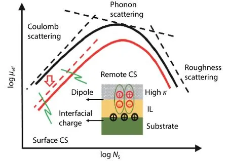
Fig.19.(Color online) A sketch of remote Coulomb scattering from charges in the gate stack.
Fig.20 shows the gate leakage current for the Ge/0.7 nm GeOx/4 nm Al2O3/Al gate stack in different PDA ambients.It can be seen that the leakage current is obviously decreased after PDA in different ambients.The leakage current reduces about one order of magnitude in N2PDA compared with the sample without PDA.NH3and O2ambients are more helpful to decrease the leakage current.This may be due to the effective passivation of the interface defect at the Ge/GeOxand GeOx/Al2O3interface.Considering the property of mobility and gate leakage current, N2PDA is more suitable for the performance improvement.
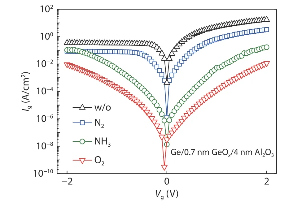
Fig.20.(Color online) Gate leakage current of Ge/0.7 nm GeOx/4 nm Al2O3/Al capacitors for different PDA ambients.
6.Conclusion
The Ge has been examined to be a very promising material with high bulk mobility to integrate into Si CMOS technology.The interface passivation, band alignment, gate charge distribution, and mobility property with Ge/GeOx/Al2O3stack by ozone oxidation are reviewed and discussed.Ozone oxidation is an effective way to obtain high Ge/GeOxinterface.Thebook=47,ebook=51band alignment of the Al2O3/Ge structure is well analyzed by gap states and CNL theory.The remote Coulomb scattering from gate charges plays a key role in mobility degradation.By extracting and modulating the charge distribution by PDA in various ambients, it is found that N2is a very proper choice to enhance the hole mobility and gate leakage current of Ge pMOSFET.The study may provide a guidance on the performance improvement of the Ge MOSFET.
Acknowledgements
This work is supported by the Natural Science Foundation of Beijing Municipality (No.4214079).
杂志排行

Journal of Semiconductors的其它文章
- High-power InAlAs/InGaAs Schottky barrier photodiodes for analog microwave signal transmission
- Twist-angle two-dimensional superlattices and their application in (opto)electronics
- A 357.9 nm GaN/AlGaN multiple quantum well ultraviolet laser diode
- All-optical switching based on self-assembled halide perovskite microwires
- Alkali metal cation engineering in organic/inorganic hybrid perovskite solar cells
- F-containing cations improve the performance of perovskite solar cells