High-threshold-voltage Normally-off Recessed MOS-gate AlGaN/GaN HEMT with Large Gate Swing
2016-09-10ZHAOYongbingZHANGYunCHENGZheHUANGYuliangZHANGLianLIUZhiqiangYIXiaoyanWANGGuohongLIJinminResearchandDevelopmentCenterforSolidStateLightingInstituteofSemiconductorsChineseAcademyofSciencesBeijing100083ChinaStateKey
ZHAO Yong-bing,ZHANG Yun,CHENG Zhe, HUANG Yu-liang,ZHANG Lian,LIU Zhi-qiang, YI Xiao-yan,WANG Guo-hong,LI Jin-min(1.Research and Development Center for Solid State Lighting,Institute of Semiconductors,Chinese Academy of Sciences,Beijing 100083,China;2.State Key Laboratory of Solid State Lighting,Beijing 100083,China;3.Beijing Engineering Research Center for The 3rd Generation Semiconductor Materials and Application,Beijing 100083,China;4.University of Chinese Academy of Sciences,Beijing 100049,China)*Corresponding Author,E-mail:yzhang34@semi.ac.cn
High-threshold-voltage Normally-off Recessed MOS-gate AlGaN/GaN HEMT with Large Gate Swing
ZHAO Yong-bing1,2,3,4,ZHANG Yun1,2,3*,CHENG Zhe1,2,3, HUANG Yu-liang1,2,3,4,ZHANG Lian1,2,3,LIU Zhi-qiang1,2,3, YI Xiao-yan1,2,3,WANG Guo-hong1,2,3,LI Jin-min1,2,3
(1.Research and Development Center for Solid State Lighting,Institute of Semiconductors,Chinese Academy of Sciences,Beijing 100083,China;2.State Key Laboratory of Solid State Lighting,Beijing 100083,China;3.Beijing Engineering Research Center for The 3rd Generation Semiconductor Materials and Application,Beijing 100083,China;4.University of Chinese Academy of Sciences,Beijing 100049,China)
*Corresponding Author,E-mail:yzhang34@semi.ac.cn
This essay has reported normally-off operation of an AlGaN/GaN recessed MOS-gate high electron mobility transistor(MOS-gate HEMT)fabricated by the inductively coupled plasma(ICP)recessed technique.A 40-nm Al2O3film was deposited by the atomic layer deposition(ALD)as the gate dielectric.The normally-off recessed MOS-gate AlGaN/GaN HEMT with a gate length of 2 μm and a gate width of 0.9 mm exhibits a high threshold voltage of +4.6 V,a specific on-resistance of 4 mΩ·cm2and a drain current density of 108 mA/mm(at a positive gate bias of 10 V).When the gate bias(Vgs)is 0 V,the breakdown voltage(BV)of 450 V has been achieved at a drain leakage current of 0.025 mA/mm for the recessed MOS-gate HEMT with a gate-drain distance of 10 μm.The on/off drain-current ratio(Ion/Ioff)is 5×10⁸for the recessed MOS-gate HEMT.Under a negative gate bias of-20 V,the gate leakage current of the recessed MOS-gate HEMT was 0.65 nA.
AlGaN/GaN;high threshold voltage;large gate swing;normally-off;specific on-resistance
1 Introduction
Owing to the outstanding properties of two-dimensional electron gases(2DEG),high electron mobility and high critical electric field[1],AlGaN/ GaN high electron mobility transistors(HEMTs)have been considered as the next-generation power semiconductor devices with high conversion efficiency,high switching frequency,and high-temperature operationcapability[2-3].However,enhancement mode operation is difficult because of normally existence of 2DEG.To achieve enhancement mode operation,many device structures have been studied,including gate recess,p-typeⅢ-nitride gate,fluorine plasma ion implantation[4-6].Many of the normallyoff AlGaN/GaN HEMTs are Schottky gate devices with relatively small threshold voltage(less than 1 V)and small gate swing.In power electronics applications,large threshold voltage(more than+3 V)and large gate swing(±10 V)are required for standard driving circuits.In order to solve these problems,a considerable AlGaN/GaN HEMT has been reported by inserting the insulating layer between the gate metal and groupⅢ-nitride surface to reduce the gate leakage current and improve the device performance[7].Metal-insulator-semiconductor(MIS)HEMT[8-10]ormetal-oxide-semiconductor(MOS)HEMT[7,11-12]with a gate dielectric has a low gate leakage current[8,13].Various dielectric materials(e.g.,A2lO[9,11],SiO2[7,12],and SiNx[8,10]) have been employed to convert Schottky gate to MIS gate or MOS gate.Additionally,the specific on-resistance(Ron)is another indispensable requirement for achieving high conversion efficiency under highvoltage switching conditions.
Atomic layer deposition(ALD)can precisely control the deposition thickness of thin films on atomic scale.The deposition of atoms is realized by the controlled saturation chemical reaction of the surface.ALD shows the advantages of good three dimensional preserving shape,100%step coverage,uniform thickness,low defect density,good adhesion,low stress,high production efficiency and low cost.Al2O3from ALD can form good Al2O3/GaN interface[9].In addition,Al2O3has wide band gap,high dielectric constant,high breakdown electric field,good thermal stability,and good chemical stability with GaN(free diffusion).
In this paper,recessed MOS-gate AlGaN/GaN HEMT with Al2O3gate dielectric is fabricated.Recessed MOS-gate AlGaN/GaN HEMT with a gatedrain distance of 10 μm delivers a high threshold voltage of+4.6 V,a drain current of 98 mA and a drain current density of 108 mA/mm at a gate bias of+10 V,a specific on-resistance of 4 mΩ·cm2and an off-state breakdown voltage of 450 V at a drain leakage current of 0.025 mA/mm with Vgs= 0 V.
2 Device Fabrication and Measurements
The AlGaN/GaN transistor structure was grown on a Si(111)substrate by metal organic chemical vapor deposition.For our sample,the barrier AlGaN layer is 26 nm thick and the Al fraction is 0.26. The Hall mobility and sheet carrier density of the 2DEG formed were 1 350 cm2/(V·s)and 0.9× 1013cm-2at room temperature,respectively.
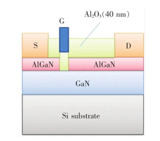
In Fig.1,the device structure of the fabricated recessed MOS-gate AlGaN/GaN HEMT is presented.TheCl2/BCl3inductivelycoupledplasma(ICP)process was used to get a electrical mesa iso-lation and gate recess.At the recessed MOS-gate region,all of AlGaN barrier layers were removed.Due to the removal of the Al0.26Ga0.74N/GaN heterostructures,the 2DEG under the gate disappears.The source-drain Ohmic metals were Ti(20 nm)/Al(40 nm)/Ti(55 nm)/Au(70 nm).These contacts were annealed at 870℃for 30 s using rapid thermal anneal in nitrogen atmosphere.The specific contact resistance was measured to be 6.5×10⁻⁵Ω·cm2by the transmission line method at room temperature. Al2O3(40 nm)film was deposited by ALD as the gate dielectric.Ni/Au(50 nm/200 nm)multilayer was e-beam evaporated as the gate metal.Si3N4film was deposited by plasma enhanced chemical vapor deposition(PECVD)for the surface passivation layer.The gate length(Lg)was 2 μm,and the gate width(Wg)was 0.9 mm(0.45 mm×2).The distance between source and gate(Lgs)was 5 μm,and the distance between gate and drain(Lgd)was 10 μm.After the device fabrication,DC characteristics of the device were measured by Keithley 4200,and the breakdown voltage(BV)was measured by Tecktronix 370A curve tracer at room temperature(300 K).

Fig.1 Cross-sectional schematic structure of recessed MOS-gate AlGaN/GaN HEMT

Fig.2 Transfer characteristics of recessed MOS-gate HEMT at Vds=0.1 V(a)and Vds=7 V(b)

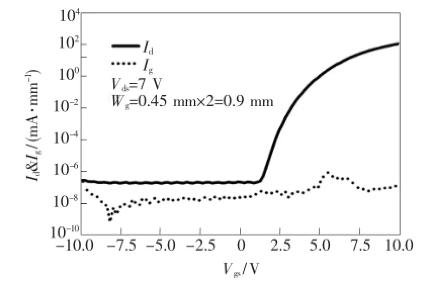
Fig.3 Transfer characteristics of recessed MOS-gate HEMT at Vds=7 V in semilog scale
3 Results and Discussion
Fig.2(a)shows the transfer I-V curve of the fabricated recessed MOS-gate HEMT at a drainsource voltage of 0.1 V.Due to the high-quality Al2O3gate dielectric and the excellent MOS interface quality in the recessed gate region,a high threshold voltage(Vth)of+4.6 V is obtained from the I-V curve.As shown in Fig.2(b),a peak transconductance of 42 mS/mm(Wg=0.9 mm)is obtained at Vgs=+10 V.
Fig.3 shows the measured off-state drain current(Ioff)at Vgs=0 V for the recessed MOS-gate HEMT at a constant drain bias of Vds=7 V.At the same time,the measured turn-on drain current(Ion)at Vgs=+10 V for the recessed MOS-gate HEMT is shown,at a constant drain bias of Vds=7 V.The on/off drain-current ratio(Ion/Ioff)is 5×10⁸for the recessed MOS-gate HEMT.
As shown in Fig.4,under a negative gate bias Vgs=-20 V,the gate leakage current of the recessed MOS-gate HEMT is 0.65 nA.The recessed MOS-gate HEMT leakage current is 225 nA at the gate bias of+12 V.Due to the good insulated property,the Al2O3dielectric film effectively suppresses the gate leakage,enabling a large gate swing from-20 V to+12 V.

Fig.4 Gate leakage current of recessed MOS-gate AlGaN/ GaN HEMT

Fig.5 On-state DC Id-Vdscharacteristics of recessed MOS-gate HEMT
The on-state DC Id-Vdscurves of the recessed MOS-gate HEMT are shown in Fig.5 with Vgsfrom 0 to+10 V.The specific on-resistance of the recessed MOS-gate HEMT is only 4 mΩ·cm2at Vgs= +10 V.Furthermore,as shown in Fig.5,at a positive gate bias of 10 V,the drain current and the drain current density of the recessed MOS-gate HEMT are 98 mA and 108 mA/mm(Wg=0.9 mm),respectively.Due to the reduced gate leakage current,much larger gate bias can be applied to the recessed MOS-gate HEMT.In order to achieve smaller specific on-resistance and larger drain current density,a relatively short gate width can be utilized.
The breakdown voltage(BV)was commonly defined when the leakage current density reaches 1 mA/mm[13].However,this criterion made the drain leakage current too high at the high operational voltage,leading to large off-state power consumption.The desired level of the leakage current was over five orders of magnitude smaller than the maximum drain current.In this work,the BV of the recessed MOS-gate HEMT was measured by a Tektronix 370A curve tracer at Vgs=0 V.As shown in Fig. 6,BV of 450 V is achieved at a drain leakage current density of 0.025 mA/mm(Peak value,bigger than the actual value significantly)for the recessed MOS-gate HEMT.

Fig.6 Off-state breakdown/leakage characteristics with Vgs=0 V.Breakdown voltage of 450 V is achieved at a drain leakage current of 0.025 mA/mm.
4 Conclusion
A normally-off recessed MOS-gate AlGaN/GaN HEMT was fabricated utilizing ICP technique.The device with Wg=0.9 mm has a high Vthof+4.6 V that is attributed to the recessed MOS-gate structure,eliminating the 2DEG under the gate region.Furthermore,a drain current of 98 mA and a drain current density of 108 mA/mm are attained at Vgs= +10 V,and the specific on-resistance is as low as 4 mΩ·cm2.The breakdown voltage is 450 V at a drain leakage current of 0.025 mA/mm with Vgs=0 V,and the gate swing is large from-20 V to+12 V.These results indicated the great potential of our fabricated normally off recessed MOS-gate AlGaN/ GaN HEMTs for power electronics applications.
References:
[1]IKEDA N,NIIYAMA Y,KAMBAYASHI H,et al..GaN power transistors on Si substrates for switching applications[J].Proc.IEEE,2010,98(7):1151-1161.
[2]CHOW T P,TYAGI R.Wide bandgap compound semiconductors for superior high-voltage unipolar power devices[J]. IEEE Trans.Electron Dev.,1994,41(8):1481-1483.
[3]TRIVEDI M,SHENAI K.Performance evaluation of high-power wide band-gap semiconductor rectifiers[J].J.Appl. Phys.,1999,85(9):6889-6897.
[4]SAITO W,TAKADA Y,KURAGUCHI M,et al..Recessed-gate structure approach toward normally off high-voltage AlGaN/GaN HEMT for power electronics applications[J].IEEE Trans.Electron Dev.,2006,53(2):356-362.
[5]CAI Y,ZHOU Y G,CHEN K J,et al..High-performance enhancement-mode AlGaN/GaN HEMTs using fluoride-based plasma treatment[J].IEEE Electron Dev.Lett.,2005,26(7):435-437.
[6]MIZUTANI T,YAMADA H,KISHIMOTO S,et al..Normally off AlGaN/GaN high electron mobility transistors with p-InGaN cap layer[J].J.Appl.Phys.,2013,113(3):034502-1-5.
[7]KHAN M A,SIMIN G,YANG J W,et al..Insulating gate III-N heterostructure field-effect transistors for high-power microwave and switching applications[J].IEEE Trans.Microw.Theory Tech.,2003,51(2):624-633.
[8]TANG Z K,JIANG Q M,LU Y Y,et al..600-V normally off SiNx/AlGaN/GaN MIS-HEMT with large gate swing and low current collapse[J].IEEE Electron Dev.Lett.,2013,34(11):1373-1375.
[9]YANG S,TANG Z K,WONG K Y,et al.High-quality interface in Al2O3/GaN/GaN/AlGaN/GaN MIS structures with in situ pre-gate plasma nitridation[J].IEEE Electron Device Lett.,2013,34(12):1497-1499.
[10]HU X,KOUDYMOV A,SIMIN G,et al..Si3N4/AlGaN/GaN-metal-insulator-semiconductor heterostructure field-effect transistors[J].Appl.Phys.Lett.,2001,79(17):2832-2834.
[11]HASHIZUME T,OOTOMO S,HASEGAWA H.Suppression of current collapse in insulated gate AlGaN/GaN heterostructure field effect transistors using ultrathin Al2O3dielectric[J].Appl.Phys.Lett.,2003,83(14):2952-2954.
[12]KHAN M A,HU X,SUMIN G,et al..AlGaN/GaN metal oxide semiconductor heterostructure field effect transistor[J]. IEEE Electron Dev.Lett.,2000,21(2):63-65.
[13]SHI J X,CHOI Y C,POPHRISTIC M,et al..High breakdown voltage AlGaN/GaN heterojunction field effect transistors on sapphire[J].Phys.Stat.Sol.(c),2008,5(6):2013-2015.

赵勇兵(1988-),男,江苏南通人,博士研究生,2011年于天津大学获得学士学位,主要从事GaN功率器件的研究。
E-mail:zhaoyongbing@semi.ac.cn

张韵(1982-),男,河北保定人,研究员,博士生导师,2011年于美国佐治亚理工学院获得博士学位,2012年入选中组部青年千人计划,主要从事GaN功率器件和GaN光电子器件的研究。
E-mail:yzhang34@semi.ac.cn
1000-7032(2016)06-0720-05
具有高阈值电压和大栅压摆幅的常关型槽栅AlGaN/GaN金属氧化物半导体高电子迁移率晶体管
赵勇兵1,2,3,4,张 韵1,2,3*,程 哲1,2,3,黄宇亮1,2,3,4,张 连1,2,3,刘志强1,2,3,伊晓燕1,2,3,王国宏1,2,3,李晋闽1,2,3
(1.中国科学院半导体研究所半导体照明研发中心,北京 100083; 2.半导体照明联合创新国家重点实验室,北京 100083;3.北京市第三代半导体材料及应用技术工程中心,北京 100083; 4.中国科学院大学,北京 100049)
介绍了一种具有高阈值电压和大栅压摆幅的常关型槽栅AlGaN/GaN金属氧化物半导体高电子迁移率晶体管。采用原子层淀积(ALD)方法实现Al2O3栅介质的沉积。槽栅常关型AlGaN/GaN MOS-HEMT的栅长(Lg)为2 μm,栅宽(Wg)为0.9 mm(0.45 mm×2),栅极和源极(Lgs)之间的距离为5 μm,栅极和漏极(Lgd)之间的距离为10 μm。在栅压为-20 V时,槽栅常关型AlGaN/GaN MOS-HEMT的栅漏电仅为0.65 nA。在栅压为+12 V时,槽栅常关型AlGaN/GaN MOS-HEMT的栅漏电为225 nA。器件的栅压摆幅为-20~+12 V。在栅压Vgs=+10 V时,槽栅常关型AlGaN/GaN MOS-HEMT电流和饱和电流密度分别达到了98 mA和108 mA/mm(Wg=0.9 mm),特征导通电阻为4 mΩ·cm2。槽栅常关型AlGaN/GaN MOS-HEMT的阈值电压为+4.6 V,开启与关断电流比达到了5×10⁸。当Vds=7 V时,器件的峰值跨导为42 mS/mm(Wg=0.9 mm,Vgs=+10 V)。在Vgs=0 V时,栅漏间距为10 μm的槽栅常关型AlGaN/GaN MOS-HEMT的关断击穿电压为450 V,关断泄露电流为0.025 mA/mm。
2016-01-21;
2016-03-07
“863”国家高技术研究发展计划(2014AA032606);国家自然科学基金(61376090,61306008)资助项目
AlGaN/GaN;高阈值电压;大栅压摆幅;常关型;特征导通电阻
10.3788/fgxb20163706.0720
TN3;TN4;TN5 Document code:A
