磁控溅射法制备ZnO:Ga薄膜的结晶质量及其应力研究
2015-12-31钟志有,兰椿,龙路等
磁控溅射法制备ZnO:Ga薄膜的结晶质量及其应力研究
钟志有1,2,兰椿1,龙路1,陆轴1
(1 中南民族大学 电子信息工程学院,武汉 430074; 2 中南民族大学 智能无线通信湖北省重点实验室, 武汉 430074)
摘要以氧化锌(ZnO)掺杂氧化镓(Ga2O3)的陶瓷靶作为溅射靶材,采用射频磁控溅射技术在玻璃衬底上制备了透明导电的掺镓氧化锌(ZnO:Ga)薄膜.通过X射线衍射仪测试研究了衬底温度对薄膜结晶性能及其残余应力的影响.研究结果表明:所有ZnO:Ga薄膜均为六角纤锌矿型的多晶结构并具有(002)方向的择优取向特性,其结晶性能和残余应力与衬底温度密切相关.随着衬底温度的升高,薄膜的(002)择优取向程度和晶粒尺寸呈现出先增大后减小的变化趋势,而薄膜的残余压应力则单调减小.当衬底温度为400℃时,ZnO:Ga薄膜具有最大的晶粒尺寸(75.1 nm)、最大的织构系数TC(002)(2.995)、较小的压应力(-0.185 GPa)和最好的结晶性能.
关键词磁控溅射;氧化锌薄膜;掺杂;结晶质量
收稿日期2014-12-26
作者简介钟志有(1965-), 男, 博士, 教授, 研究方向: 光电子材料及其器件, E-mail: zhongzhiyou@163.com
基金项目湖北省自然科学基金资助项目(2011CDB418); 中央高校基本科研业务费专项资金资助项目(CZW14019)
中图分类号TM914文献标识码A
The Crystal Quality and Residual Stress of ZnO:Ga Thin
Films Prepared by Magnetron Sputtering Method
ZhongZhiyou1,2,LanChun1,LongLu1,LuZhou1
(1 College of Electronic Information Engineering, South-Central University for Nationalities, Wuhan 430074, China;
2 Hubei Key Laboratory of Intelligent Wireless Communications,South-Central University for Nationalities,Wuhan 430074,China)
AbstractThe gallium-doped zinc oxide (ZnO:Ga) thin films were prepared on glass substrates by magnetron sputtering method using the ceramic target fabricated by sintering the mixture of ZnO and Ga2O3 nanometer powder. The substrate temperature was varied from 200 ℃ to 500 ℃ during the magnetron sputtering process. The crystal quality and residual stress of the deposited films were investigated by X-ray diffractometer. The results indicated that the crystal quality and residual stress of the samples are closely related to the substrate temperature. As the substrate temperature increasing, the degree of preferred orientation, average grain size and residual stress of the samples change nonmonotonically. The thin film deposited at the substrate temperature of 400 ℃ has the largest grain size (75.1 nm), the maximum texture coefficient TC(002) (2.995), the lower compressive stress (-0.185 GPa) and the best crystal quality.
Keywordsmagnetron sputtering; zinc oxide thin films; doping; crystal quality
透明导电氧化物(TCO)薄膜由于具有良好的可见光透过率和较低的电阻率,因而在平板显示[1-6]、传感器[7-9]、太阳能电池[10-15]、发光二极管[16-19]和声表面波器件[20,21]等领域有着广阔的应用前景.众所周知,掺锡氧化铟(In2O3:Sn)作为TCO薄膜家族中的重要成员,因其具有优越的光电性能而被人们深入研究并得到了广泛应用,但是由于该TCO薄膜中的铟为稀有金属、自然储量有限、价格昂贵且有毒性,从而限制了In2O3:Sn薄膜的使用范围,所以寻找其替代产品已经成为当前TCO薄膜领域的一个重要研究课题.与当前主流产品In2O3:Sn相比,掺镓氧化锌(ZnO:Ga)薄膜作为一种直接跃迁的宽带隙TCO半导体材料,具有资源丰富、价格低廉、性能稳定、没有毒性等特点,因此近年来深受各国研究者的青睐,被普遍认为它是值得研发的新一代TCO材料之一.当前,ZnO:Ga薄膜的主要制备技术有水热法[22]、喷雾热分解[23,24]、脉冲激光沉积[25,26]、磁控溅射[27-33]、溶胶-凝胶[34,35]和原子层沉积[36,37]等,其中磁控溅射工艺具有沉积速度快、制备薄膜致密度高、附着性能好和易于实现大面积成膜等特点[38,39],因此它是目前制备ZnO:Ga薄膜的最常用沉积技术之一.此前广大研究者围绕ZnO:Ga薄膜的生长技术、制备工艺、微观结构和光电性能等方面开展了大量的研究工作,结果表明,衬底温度是影响ZnO:Ga薄膜结构和光电性能的重要工艺参数之一,从现有文献报道来看,人们的研究重点主要集中在衬底温度对ZnO:Ga薄膜的微观结构和光电性能的影响,而对ZnO:Ga薄膜应力的研究却报道较少.事实上,薄膜应力的存在会导致薄膜的破裂、脱落或者使衬底发生形变,从而直接影响薄膜器件的光学、电学、磁学、力学和使用寿命等性能[40,41],薄膜应力是一个必须考虑而且需要最终控制的参量,因此了解和控制薄膜应力的影响对于器件设计和使用是非常重要的.本文以普通玻璃作为衬底材料,采用磁控溅射工艺制备了ZnO:Ga半导体薄膜,重点研究了衬底温度对ZnO:Ga薄膜结晶质量及其应力的影响.
1实验部分
1.1衬底处理
选用普通玻璃作为衬底材料,首先采用丙酮擦拭玻璃衬底表面,然后用清水冲洗干净,再依次使用丙酮、无水乙醇和去离子水各超声清洗约15 min,最后在无水乙醇中煮沸,吹干待用.
1.2薄膜制备
利用射频磁控溅射技术在玻璃衬底上沉积ZnO:Ga薄膜样品,所用实验设备为国产KDJ-567型高真空复合镀膜系统,所用溅射靶材的直径为5.0 cm、厚度为0.4 cm,它由ZnO(98 wt.%)和Ga2O3(3 wt.%)混合烧结而成,ZnO和Ga2O3的纯度均为99.99%.溅射气体为高纯氩气(纯度:99.99 %),在ZnO:Ga 薄膜沉积之前,先将玻璃衬底放置于镀膜系统的真空室中,待气压抽至大约5.0×10⁻⁴Pa后通入氩气,并先采用氩等离子体对衬底表面处理5 min,然后再对靶材表面预溅射10 min以去除其表面的杂质和污染物.本实验中,制备ZnO:Ga半导体薄膜的工艺参数如下:靶材表面与衬底之间的距离为0.7 cm,射频功率为170 W,工作压强为0.5 Pa,氩气流量为15 sccm,沉积时间为25 min.为了研究衬底温度对ZnO:Ga薄膜性能的影响,实验过程中调节衬底温度分别为200 ℃、300 ℃、400 ℃和500 ℃制备薄膜样品,并将它们标记为S1、S2、S3和S4.
1.3表征技术
在室温(约25 ℃)和大气条件下,通过德国Bruker公司生产的D8-ADVANCE型X射线衍射仪表征薄膜样品的晶体结构,测试时所用辐射源为CuKα(λ=0.1541 nm),采用θ-2θ连续扫描方式,扫描角度为20~60°,扫描间隔为0.0167°,扫描速度为10 °/min,工作电压为40 kV,工作电流为40 mA.
2结果与讨论
图1为不同衬底温度时所制备ZnO:Ga薄膜样品的XRD图谱,由图1可见,在20~60°的扫描范围内,所有样品都存在3个较强的衍射峰,其2θ位于31.5°、34.4°和56.2°附近,它们分别对应于ZnO的(100)、(002)和(110)特征谱线,该结果与标准ZnO(JCPDS No. 36-1451)峰位数据相吻合[42,43],另外在图1中没有观察到金属Ga、Zn及其化合物的特征衍射峰,这些结果表明:Ga替代了Zn的位置,或者存在于六角晶格之中,或者分布在晶粒间界的区域,在XRD检测范围内没有生成其它新的物相,所有薄膜样品均为单相的六角纤锌矿型ZnO多晶结构.观察图1中ZnO:Ga样品的衍射峰强度可以看出,所有薄膜的(002)衍射峰强度均远远大于其它衍射峰的强度,结果说明所制备的ZnO:Ga样品沿(002)方向均具有明显的结晶择优取向性.
表1总结了不同衬底温度下所制备ZnO:Ga薄膜样品的衍射峰强度,可以看出,衬底温度升高时,(100)和(110)衍射峰的强度变化不明显,而(002)衍射峰的强度(I(002))变化却很显著,由表1可见,当衬底温度从200 ℃升高到400 ℃时,(002)峰的衍射强度(I(002))大幅度增加,但是当衬底温度进一步从400 ℃升高至500 ℃时,(002)峰的衍射强度I(002)反而减小.当衬底温度为400 ℃时,ZnO:Ga薄膜具有最大的(002)衍射峰强,高达28303 cps.(002)晶面的衍射强度I(002)与薄膜沿c轴垂直于衬底的生长取向密切相关,这种结晶取向有利于电荷的迁移.

图1 所有ZnO:Ga样品的XRD图谱 Fig.1 XRD patterns of all the ZnO:Ga samples

样品I(100)/cpsI(002)/cpsI(110)/cpsS14122298S238271011S353283039S432907110
根据Mueller修正的Harris方法,可以采用(hkl)晶面的织构系数(TC(hkl))来衡量晶体的择优取向程度,TC(hkl)的数值越大,则说明(hkl)晶面的择优取向程度就越高.根据文献[44],TC(hkl)的计算公式定义如下:

(1)
(1)式中,h、k、l为衍射晶面指数,TC(hkl)为(hkl)晶面的织构系数,I(hkl)和I0(hkl)分别为薄膜样品与标准ZnO样品(JCPDS No. 36-1451)在(hkl)晶面的衍射峰强度,N为计算时所取的衍射峰数目.根据XRD测试数据可以计算ZnO:Ga薄膜样品各个晶面(hkl)的织构系数TC(hkl)数据.图2给出了所有ZnO:Ga样品三个晶面(100)、(002)和(110)的织构系数TC(100)、TC(002)和TC(110),由图2可知,对于这些样品,其TC(100)小于0.03、TC(110)小于0.02,而TC(002)则大于2.95,即TC(002)的数值远远大于TC(100)和TC(110),说明了本实验所制备的ZnO:Ga薄膜都具有明显的(002)晶面择优取向生长特性.从图2还可看出,衬底温度的变化对TC(002)数值也具有明显的影响,当衬底温度从200 ℃升高至500 ℃时,织构系数TC(002)的值呈现出“先增加、后减小”的变化趋势,当衬底温度为400 ℃时,ZnO:Ga薄膜具有最大的TC(002)值(2.995),其(002)晶面的择优取向程度最高.

图2 所有ZnO:Ga样品的TC (100), TC (002)和TC (110)数值 Fig.2 The values of TC (100), TC (002) and TC (110) of all the ZnO:Ga samples

图3 所有ZnO:Ga样品的2θ, B和D数值 Fig.3 The values of 2θ, B and D of all the ZnO:Ga samples
图3(a)和(b)分别给出了薄膜样品(002)峰位2θ和对应的半高宽(B)数据,随着衬底温度的升高,2θ值逐渐增大,当温度高于400 ℃时其变化不明显;而B值则是先迅速减小而后略有增大.结果表明:衬底温度为400 ℃时,ZnO:Ga样品具有合适的(002)峰位2θ值和最小的(002)峰半高宽B,所对应薄膜的结晶质量最佳.薄膜样品的平均晶粒尺寸(D)可以根据Debye-Scherrer公式[45,46]计算获得:

(2)
(2)式中,λ为X射线波长(λ=0.1541 nm),θ为最大衍射峰(002)晶面的Bragg角,B为对应的半高宽,θ和B的单位为度(°).基于(002)晶面的XRD数据,可得所有样品的平均晶粒尺寸D如图3(c)所示,由图可见,晶粒尺寸D与衬底温度密切相关,当衬底温度从300 ℃升高至400 ℃时,薄膜的晶粒尺寸D迅速增大(75.1 nm),但当衬底温度继续升高时,其晶粒尺寸D却明显减小,其原因在于:适当提高衬底温度能够使溅射出来的原子/原子团更容易形成小岛,或更进一步产生小岛并联,从而导致晶粒增大.上述结果表明:选择合适的衬底温度对于ZnO:Ga薄膜的制备是非常重要的.
薄膜样品的(002)峰的晶面间距(d)可由Bragg公式[47]计算:
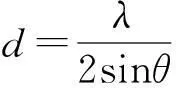
(3)
由于ZnO为六角纤锌矿结构,(hkl)晶面的晶格常数(c)可以根据方程(4)确定[47]:

(4)
对于ZnO的(002)晶面,其晶格常数c=2d.图4给出了所有薄膜样品(002)峰所对应的晶面间距d和晶格常数c,可以看到,薄膜样品的d和c均大于标准ZnO(JCPDS No. 36-1451)的数值(d0=0.2603 nm,c0=0.5206 nm)[42],并且它们随着衬底温度的升高而减小并逐渐接近于标准ZnO的数值.这是因为:衬底温度升高时,沉积粒子的能量增大,从而导致成膜时粒子更容易达到平衡位置,因此使得晶粒内部应力能够更好地被释放掉.根据Double-axis Stress模型[48],薄膜的残余应力(σf)可利用如下公式计算:

(5)

(6)
在(5)、(6)式中,Cij为标准ZnO样品的弹性模量值[48],其中C11=208.8 GPa,C12=119.7 GPa,C13=104.2 GPa,C33=213.8 GPa,ε为薄膜样品(002)方向的相对应变,c0和c分别表示标准样品与薄膜样品的晶格常数.由(5)式和(6)式可得,残余应力σf可以表示为:
σf=-232.8ε(GPa),
(7)
实际上,薄膜的残余应力σf是各种因素所引起应力分量的总和,这些应力分量包括起源于薄膜生长过程中的结构不完整性(如杂质、空位、晶粒边界、位错和层错等)、表面能态的存在和薄膜与衬底界面之间的晶格错配等诸多因素所决定的内应力(σin),以及薄膜与衬底的热膨胀系数不同所引起的热应力(σth),即有:
σf=σin+σth,
(8)
(8)式中,热应力σth由下式确定[49]:
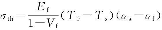
(9)
(9)式中,Ef和νf为薄膜样品杨式模量和泊松比,T0和Ts分别为样品测量时的环境温度和制备薄膜时的温度,αs和αf分别为衬底和薄膜样品的热膨胀系数.图5给出了所有薄膜样品的残余应力σf和热应力σth数据,可以看出,这些样品的σf和σth均为负值,说明了薄膜的残余应力和热应力都为压应力.随着衬底温度的升高,σf值和σth值的变化趋势相反,即σf值减小而σth值增大.例如:当衬底温度从200 ℃升高到400 ℃时,σf值由2.653 GPa减小为0.185 GPa、σth值由0.117 GPa增大为0.250 GPa,可见,当衬底温度较低时,σf值比σth值大得多,这表明残余应力σf主要决定于薄膜的内应力、而热应力σth的作用可以忽略;但是当衬底温度较高时,热应力σth对残余应力σf的贡献大大增加,其影响却不能忽略.衬底温度较低时,沉积的ZnO:Ga薄膜中存在较多的间隙锌原子和氧空位,从而导致薄膜沿c轴方向存在较大的压应力,而随着衬底温度的升高,吸附于衬底表面的原子迁移能力增强,沉积原子更容易迁移到晶格中的平衡位置并改善薄膜的结晶质量,进而减少了薄膜中的锌间隙,因此使薄膜中的压应力得以释放.

图4 所有ZnO:Ga样品的d和c数值 Fig.4 The values of d and c of all the ZnO:Ga samples

图5 所有ZnO:Ga样品的σ f和σ th数值 Fig.5 The values of σ f and σ th of all the ZnO:Ga samples
3结语
采用高密度ZnO掺杂Ga2O3的陶瓷靶作为溅射源材料,利用射频磁控溅射方法在普通玻璃衬底上沉积了ZnO:Ga半导体薄膜,研究了衬底温度对薄膜样品的结晶质量和残余应力的影响.实验结果显示:所有薄膜样品都为六角纤锌矿型的多晶结构,并具有(002)方向的择优取向生长特性.衬底温度对薄膜的结晶性能和残余应力具有显著性的影响,随着衬底温度的升高,ZnO:Ga薄膜的(002)择优取向程度和平均晶粒尺寸都呈现“先增后减”的变化趋势,而薄膜的残余压应力数值则单调减小.当衬底温度为400 ℃时薄膜具有较小的压应力、最大的织构系数TC(002)和最好的结晶性能.这些结果表明选择合适的衬底温度对于沉积ZnO:Ga半导体薄膜是至关重要的.
参考文献
[1]Burroughes J H, Bradley D D C, Brown A R, et al. Light-emitting diodes based on conjugated polymers [J]. Nature, 1990, 347 (6293): 539-541.
[2]Tang C W, VanSlyke S A. Organic electroluminescent diodes [J]. Appl Phys Lett, 1987, 51 (12): 913-915.
[3]Zhong Z Y, Jiang Y D. Surface treatments of indium-tin oxide substrates for polymer electroluminescent devices [J]. Phys Status Solidi A, 2006, 203 (15): 3882-3892.
[4]陈首部, 韦世良, 何翔, 等. 改性方法对氧化铟锡衬底表面形貌和化学组分的影响 [J]. 中南民族大学学报: 自然科学版, 2009, 28 (4): 43-46.
[5]You Z Z,Hua G J,Lou S F.Optoelectrical characteristics of organic light-emitting devices fabricated with different cathodes [J]. Int J Electron, 2011, 98 (1): 129-135.
[6]马涛, 黄毅, 马健, 等. 溶胶-凝胶法制备CuAlO2多晶的结构性能研究 [J]. 西南民族大学学报: 自然科学版, 2012, 38 (5): 819-821.
[7]Patel N G, Patel P D, Vaishnav V S. Indium tin oxide (ITO) thin film gas sensor for detection of methanol at room temperature [J]. Sensor Actuat B-Chem, 2003, 96 (1-2): 180-189.
[8]Yi I-J, Kim J-H, Choi Y J, et al. A disposable biosensor with Prussian blue deposited electrode [J]. Microelectron Eng, 2006, 83 (4-9): 1594-1597.
[9]Mitsubayashi K, Wakabayashi Y, Tanimoto S, et al. Optical-transparent and flexible glucose sensor with ITO electrode [J]. Biosens Bioelectron, 2003, 19 (1): 67-71.
[10]刘霄, 曾广根, 张静全, 等. 反应磁控溅射制备CdTe太阳电池前电极ITO薄膜的性质研究 [J]. 西南民族大学学报: 自然科学版, 2014, 40 (2): 265-270.
[11]Tang C W. Two-layer organic photovoltaic cell [J]. Appl Phys Lett, 1986, 48 (2): 183-185.
[12]Kim J Y, Lee K, Coates N E, et al. Tandem polymer solar cells fabricated by all-solution processing [J]. Science, 2007, 317 (5835): 222-225.
[13]李襄宏, 唐定国. 基于1,10-邻菲罗啉衍生物的两亲性钌配合物的合成及其光电转化性质 [J]. 中南民族大学学报: 自然科学版, 2009, 28 (3): 9-13.
[14]Sio A D, Chakanga K, Sergeev O, et al. ITO-free inverted polymer solar cells with ZnO:Al cathodes and stable top anodes [J]. Sol Energy Mater Sol Cells, 2012, 98 (1): 52-56.
[15]顾锦华,钟志有,何翔,等.真空退火处理对光敏薄膜及聚合物太阳电池性能的影响[J].中南民族大学学报:自然科学版,2009,28(3):30-33.
[16]Kim H, Horwitz J S, Kim W H, et al. Doped ZnO thin films as anode materials for organic light-emitting diodes [J]. Thin Solid Films, 2002, 420-421: 539-543.
[17]Cao H T, Sun C, Pei Z L, et al. Properties of transparent conducting ZnO:Al oxide thin films and their application for molecular organic light-emitting diodes [J]. J Mater Sci: Mater Electron, 2004, 14 (1): 169-174.
[18]Kim H, Piqué A, Horwitz J S, et al. Effect of aluminum doping on zinc oxide thin films grown by pulsed laser deposition for organic light-emitting devices [J]. Thin Solid Films, 2000, 377-378 (1): 798-802.
[19]孙奉娄, 惠述伟. 衬底温度对射频溅射沉积ZAO透明导电薄膜性能的影响 [J]. 中南民族大学学报: 自然科学版, 2009, 28 (2): 10-13.
[20]Shih W-C,Wang T-L,Pen Y-K.Enhancement of characteristics of ZnO thin film surface acoustic wave device on glass substrate by introducing an alumina film interlayer [J]. App Surf Sci, 2012, 258 (9): 5424-5428.
[21]Phan D-T, Chung G-S. Fabrication and characteristics of a surface acoustic wave UV sensor based on ZnO thin films grown on a polycrystalline 3C-SiC buffer layer [J]. Curr Appl Phys, 2012, 12 (3): 521-524.
[22]Guo J, Zheng J, Song X, et al. Synthesis and conductive properties of Ga-doped ZnO nanosheets by the hydrothermal method [J]. Mater Lett, 2013, 97 (1): 34-36.
[23]Rao T P, Kumar M C S, Hussain N S. Effects of thickness and atmospheric annealing on structural, electrical and optical properties of GZO thin films by spray pyrolysis [J]. J Alloy Compd, 2012, 541 (2): 495-504.
[24]Reddy K T R, Reddy T B S, Forbes I,et al. Highly oriented and conducting ZnO:Ga layers grown by chemical spray pyrolysis [J]. Surf Coat Technol, 2002, 151-152 (1): 110-113.
[25]Minami T, Miyata T, Ohtani Y, et al. Effect of thickness on the stability of transparent conducting impurity-doped ZnO thin films in a high humidity environment [J]. Phys Status Solidi R, 2007, 1(1): R31-R33.
[26]Kim H, Horwitz J S, Kim W H, et al. Doped ZnO thin films as anode materials for organic light-emitting diodes [J]. Thin Solid Films, 2002, 420-421 (2): 539-543.
[27]Wang L, Swensen J S, Polikarpov E, et al. Highly efficient blue organic light-emitting devices with indium-free transparent anode on flexible substrates [J]. Org Electron, 2010, 11: 1555-1560.
[28]Gorrie C W, Sigdel A K, Berry J J, et al. Effect of deposition distance and temperature on electrical, optical and structural properties of radio-frequency magnetron-sputtered gallium-doped zinc oxide [J]. Thin Solid Films, 2010, 519 (1): 190-196.
[29]Liu H, Fang L, Tian D, et al. Different magnetothermoelectric behavior in Al- and Ga-doped ZnO thin films [J]. J Alloy Compd, 2014, 588 (2): 370-373.
[30]Kim Y H, Jeong J, Lee K S, et al. Effect of composition and deposition temperature on the characteristics of Ga doped ZnO thin films [J]. Appl Surf Sci, 2010, 257 (1): 109-115.
[31]Bie X, Lu J, Wang Y, et al. Optimization of parameters for deposition of Ga-doped ZnO films by DC reactive magnetron sputtering using Taguchi method [J]. Appl Surf Sci, 2011, 257 (10): 6125-6128.
[32]Park H-K, Kang J-W, Na S-I, et al. Characteristics of indium-free GZO/Ag/GZO and AZO/Ag/AZO multilayer electrode grown by dual target DC sputtering at room temperature for low-cost organic photovoltaics [J]. Sol Energy Mater Sol Cells, 2009, 93 (7): 1994-2002.
[33]Lin Y C, Yen W T, Shen C H, et al. Surface texturing of Ga-doped ZnO thin films by pulsed direct-current magnetron sputtering for photovoltaic applications [J]. J Electron Mater, 2012, 41(3): 442-450.
[34]Tsay C-Y, Wu C-W, Lei C-M, et al. Microstructural and optical properties of Ga-doped ZnO semiconductor thin films prepared by sol-gel process [J]. Thin Solid Films, 2010, 519 (6): 1516-1520.
[35]Tsay C-Y, Fan K-S, Lei C-M. Synthesis and characterization of sol-gel derived gallium-doped zinc oxide thin films [J]. J Alloy Compd, 2012, 512 (1): 216-222.
[36]Nam T, Lee C W, Kim H J, et al. Growth characteristics and properties of Ga-doped ZnO (GZO) thin films grown by thermal and plasma-enhanced atomic layer deposition [J]. Appl Surf Sci, 2014, 295 (2): 260-265.
[37]Saito K, Hiratsuka Y, Omata A, et al. Atomic layer deposition and characterization of Ga-doped ZnO thin films [J]. Superlattice Microst, 2007, 42 (1): 172-175.
[38]You Z Z, Hua G J. Structural, optical and electrical characterization of ZnO:Ga thin films for organic photovoltaic applications [J]. Mater Lett, 2011, 65 (1): 3234-3236.
[39]林庆祥, 黄毅. P型透明导电氧化物CuAlO2的研究进展[J]. 西南民族大学学报: 自然科学版, 2014, 40 (2): 256-260.
[40]Zheng X, Li J, Zhou Y. X-ray diffraction measurement of residual stress in PZT thin films prepared by pulsed laser deposition [J]. Acta Mater, 2004, 52 (5): 3313-3322.
[41]Hsiao C C, Hu Y C, Chang R C, et al. Residual stresses and mechanical properties of a ZnO pyroelectric sensor [J]. Theor Appl Fract Mech, 2009, 52 (1): 1-6.
[42]Raoufi D, Raoufi T. The effect of heat treatment on the physical properties of sol-gel derived ZnO thin films [J]. Appl Surf Sci, 2009, 255 (7): 5812-5817.
[43]Zhong Z Y, Zhang T. Microstructure and optoelectronic properties of titanium-doped ZnO thin films prepared by magnetron sputtering [J]. Mater Lett, 2013, 96 (2): 237-239.
[44]Valle G G, Hammer P, Pulcinelli S H, et al. Transparent and conductive ZnO:Al thin films prepared by sol-gel dip-coating [J]. J Eur Ceram Soc, 2004, 24 (4): 1009-1013.
[45]Hong R, Shao J, He H, et al. ZnO:Zn phosphor thin films prepared by face-to-face annealing [J]. J Cryst Growth, 2005, 284 (3-4) 347-352.
[46]黄涛, 李灿, 吴静, 等. 四方形钯纳米片的控制合成 [J]. 中南民族大学学报: 自然科学版, 2013, 32 (3): 5-7.
[47]Zhang T, Zhong Z. Effect of working pressure on the structural, optical and electrical properties of titanium-gallium co-doped zinc oxide thin films[J]. Mater Sci-Poland, 2013, 31(3): 454-461.
[48]Swapna R, Kumar M C S, The role of substrate temperature on the properties of nanocrystalline Mo doped ZnO thin films by spray pyrolysis [J]. Ceram Int, 2012, 38 (5): 3875-3883.
[49]Conchon F, Renault P O, Bourhis E L, et al. X-ray diffraction study of thermal stress relaxation in ZnO films deposited by magnetron sputtering [J]. Thin Solid Films, 2010, 519 (6): 1563-1567.