Enhanced thermal emission from metal-free,fully epitaxial structures with epsilon-near-zero InAs layers
2024-03-02KarolisStaysAndrejusGeiutisandJanDevenson
Karolis Stašys,Andrejus Geižutis,and Jan Devenson
State Research Institute Center for Physical Sciences and Technology,Savanorių ave.231,LT-02300 Vilnius,Lithuania
Abstract: We introduce a novel method to create mid-infrared (MIR) thermal emitters using fully epitaxial,metal-free structures.Through the strategic use of epsilon-near-zero (ENZ) thin films in InAs layers,we achieve a narrow-band,wide-angle,and p-polarized thermal emission spectra.This approach,employing molecular beam epitaxy,circumvents the complexities associated with current layered structures and yields temperature-resistant emission wavelengths.Our findings contribute a promising route towards simpler,more efficient MIR optoelectronic devices.
Key words: epsilon-near-zero;thermal emitters;indium arsenide;LWIR (long wave infraRed);molecular beam epitaxy
1.Introduction
The mid-infrared (MIR) spectrum,delineated by wavelengths ranging from 2 to 15μm,is of paramount importance due to its overlap with fundamental rotational and vibrational transitions of technologically-relevant molecules[1].This overlap has catalyzed an increased demand for high-efficiency MIR radiation sources,notably those emitting between 4 and 10μm,with ramifications spanning across environmental monitoring,medical diagnostics,defense mechanisms,and advanced industrial applications.
Historically,while the potential applications of the MIR spectrum have been vast,the paucity of diverse and efficient optoelectronic devices has posed a formidable challenge.This technological void was partially addressed with the seminal introduction of the quantum cascade laser (QCL) in the mid-1990s[2].Utilizing the intrinsic properties of semiconductor heterostructures,namely InP,InAs,and GaAs,QCLs extended the operational wavelength range from 3 to beyond 10μm.Notwithstanding this advancement,the intricate heterostructural design,characterized by myriad epitaxial layers,has perpetuated the quest for more pragmatic and efficient MIR device architectures.
Contemporary research trends accentuate the potential of thermal emitters in the extended MIR spectrum.Standard thermal emitters,characterized by their broad and omnidirectional spectra,can be meticulously engineered at the nanoscale to achieve tailored emissivity profiles[3,4].Epsilonnear-zero (ENZ) thin films have emerged as frontrunners in this domain,with their idiosyncratic dispersion properties facilitating a narrowband,p-polarized thermal emission spectrum[5].Crucially,the Berreman mode in these films has demonstrated a propensity for inducing spectrally confined leaky radiation,an attribute underpinned by its intrinsic flat dispersion characteristics[6].Concurrently,recent advancements in nanophotonic material design have elucidated the potential of spatially-graded ENZ materials.Such structures,when epitaxially grown with doped Ⅲ–Ⅴ group semiconductors like InAs,have manifested a paradigm shift in controlling both the spectral and directional attributes of emitted thermal radiation[7].
In parallel to these approaches,research has ventured into the realm of plasmonic metastructures.Specifically,strategies revolving around plasmonic Brewster funneling and adiabatic plasmonic focusing have been heralded for realizing ultra-broadband omnidirectional absorbers and angularly selective coherent thermal emitters.Such designs,while pioneering,hinge on properly patterned complex metastructures and seek to amalgamate inherently non-resonant effects to achieve broadband absorption and emission across terahertz,infrared,and optical frequencies[8].Although these metastructures offer a broad spectrum,their intricacies in design and fabrication might pose challenges,especially in scaling and practical application scenarios.
Conversely,the focus of our investigation is on epitaxial architectures that provide an attractive alternative to these intricate patterned systems.We posit that our emitters,devoid of such elaborate patterning,not only simplify the design and growth processes but potentially offer advantages in terms of scalability,robustness,and application versatility.
Yet,the path to full MIR spectrum exploitation is laden with challenges.The realization of desired plasma frequencies,notably in the vicinity of 6µm,remains elusive.InSbbased materials,albeit promising due to their low effective electron mass,grapple with challenges inherent to epitaxial growth,especially when interfaced with substrates like GaSb and InAs[9].Compounding this complexity are recent observations alluding to the violation of Kirchhoff's law in ultrathin magnetized InAs films operating at ENZ frequencies,a discovery that could revolutionize our foundational understanding of thermoradiative processes[10].
Positioned within this intricate scientific landscape,our investigation harnesses the unique electronic properties of InAs.Characterized by a low electron effective mass and an intrinsic compatibility with GaSb and InAs substrates,InAs,especially in its low-temperature-grown form (LT-InAs),exhibits a remarkable free carrier density even in the absence of extrinsic doping[11].This research elucidates the spectral properties of novel MIR emitters,each architecturally defined by two heavily doped epitaxial layers separated by a spacer,grown by molecular beam epitaxy (MBE).
2.Molecular beam epitaxy grown samples
Leveraging the distinctive properties of epsilon-near-zero(ENZ) thin films,the samples used in this study were designed to capitalize on the unique dispersion characteristics of leaky plasmon polaritons,thereby generating a narrowband,wide-angle,p-polarized thermal emission spectrum.The central structure of these samples involves two heavily doped epitaxial layers separated by a spacer layer.Through meticulous control of the doping levels,the plasma resonance frequency was manipulated,determining the emission wavelength.These samples were grown on n-InAs (100)and p-GaSb (100) substrates using a Veeco GENxplor MBE reactor,enabling the production of mid-infrared light sources that can emit at variable wavelengths.The variability in the emission wavelength is contingent on the free electron density in the InAs layers,thereby introducing a novel technique in designing light sources for different mid-infrared emission wavelengths.
Two unique types of samples were grown on n-InAs(100) and p-GaSb (100) substrates via a Veeco GENxplor MBE reactor.This reactor was furnished with conventional Al,In,and Ga group Ⅲ lemental sources and As and Sb crackers for group V elemental sources.The growth temperature was controlled using thek-space associates BandiT temperature monitoring system,based on pyrometry and absorption edge spectroscopic measurements.Surface reconstructions,which occurred during the thermal oxide removal process and the epitaxial layer growth,were monitored using a Staib RHEED system.
The sample VGS0055,grown on a GaSb substrate,comprised a 100 nm undoped GaSb buffer layer,grown at a temperature of 520 °C.It was topped with a 100 nm AlSb layer and a 1µm n-doped (N=5 × 1019cm-3) InAs layer,both grown at 505 °C.This was followed by a 500 nm undoped AlSb layer and a second 1µm thick n-doped (N=5 ×1019cm-3) InAs layer,both grown at a reduced temperature of 450 °C to prevent interdiffusion at the interfaces.
The sample VIA0027,grown on an InAs substrate,exhibited a structure comparable to that on GaSb.It featured an initial 100 nm undoped InAs layer,followed by a 1µm n-doped(N=6.5 × 1019cm-3) InAs layer,a 500 nm AlAsSb layer,and a second 1µm n-doped (N=6.5 × 1019cm-3) InAs layer.Mirroring the GaSb-based structure,the growth temperatures for both the AlAsSb layer and the second n-InAs layer were reduced to 450 °C.In contrast,the initial InAs layer was grown at a higher temperature of 505 °C.Extra arsenic was added into AlSb to match the crystal lattice period to the InAs substrate,enhancing the crystalline quality.
The oxide removal process for GaSb and InAs substrates necessitated temperatures of 545 and 525 °C,respectively.An Sb beam equivalent pressure (BEP) of 6.5 × 10⁻⁶Torr was maintained for the GaSb oxide removal,while an As BEP of 1.2 ×10⁻⁵Torr was employed for the InAs substrates.Different doping levels were assigned to the n-InAs layers,regulated by adjusting the Si source temperatures.The achieved doping levels were subsequently confirmed through Hall measurements.The designs of the grown sample structure are revealed in Fig.1.

Fig.1.(Color online) Structure of samples grown using molecular beam epitaxy.
3.Experiment setup
Samples crystal quality and uniformity of layers was determined from measured X-ray diffraction (XRD) spectra.XRD curves were measured by Smartlab (Rigaku) diffractometer equipped with Ge (400) 2-bounce monochromator (for Cu Kα1 X-ray wavelength of 1.5406 Å) and scintillation detector SC-70 (for 2D measurements linear D/tex Ultra detector was used).Surface morphology and defects were investigated from differential interference contrast microscopy (Nomarski microscopy) images.These images were taken using BX53m(Olympus) microscopy system with digital camera.
In the preliminary investigations,emission from the prepared samples was measured using a conventional photoluminescence (PL) setup.The sample surfaces were illuminated with a 3 W diode-pumped solid-state (DPSS) laser,modulated at 1 kHz and emitting at 808 nm.A parabolic mirror was employed to collect the emitted light and collimate the beam towards the spectrometer.The emission spectra were examined with a BRUKER vertex V80 Fourier transform infrared (FTIR) spectrometer operating in amplitude modulation step-scan mode,with a liquid nitrogen-cooled mercury cadmium telluride (MCT) detector in place.The measurement of thermal emission necessitated the attachment of the sample to a PID-controlled heater,a screen plate with a 5 mm aperture was placed in front of the epi-side of the wafer,and a light chopper was utilized to modulate the emission.The experimental setup scheme is presented in Fig.2.

Fig.2.(Color online) Experimental setup for powering-up the epitaxial structures and measuring thermal emission.
Plasma resonance was evaluated using the 10° reflection measurement accessory of the Bruker spectrometer.For these reflection measurements,a thermal Globar light source and a Deuterated Triglycine Sulphate (DTGS) detector were used.
4.Results and discussion
High-resolution X-ray diffraction (XRD) rocking curves for samples VGS0055 and VIA0027 are depicted in Fig.3.The blue curves represent actual measurements,while the red ones correspond to simulation results.Notably,the sample VGS0055 displays significant relaxation,approximately 5% for the InAs layer and around 30% for the AlSb layer.Conversely,the introduction of some amount of As during the growth of the AlSb layer in sample VIA0027 mitigated the lattice mismatch between InAs and AlSb layers.X-ray diffraction simulations indicate that roughly 10% of As was incorporated into the AlSb layer,and all layers were grown without relaxation.As a result,the surface of sample VIA0027 was notably smoother compared to sample VGS0055.

Fig.3.(Color online) High-resolution X-ray diffraction rocking curves from samples VGS0055 (a) (grown on a GaSb substrate) and VIA0027 (b)(grown on an InAs substrate).
Surface morphology was examined using Nomarski microscopy,with the captured images showcased in Fig.4.Observations from the Nomarski images reveal that both samples have grid-like structures,with rows aligned to the [011]and [01] directions.Consistent with the X-ray diffraction findings,the pronounced relaxation in sample VGS0055 resulted in more pronounced dislocation rows.A clear predominance of dislocations along the [011] direction is evident in both samples.
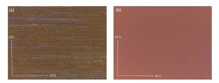
Fig.4.(Color online) Nomarski microscopy surface images of the samples VGS0055 (a) and VIA0027 (b).The scale bar at the bottom right represents 20 µm.

Fig.5.(Color online) Reflectance (black) and thermal emission (red) spectra measured on samples VGS0055 (a) and VIA0027 (b).
The doping levels of both samples were confirmed using Hall effect measurements.Sample VIA0027’s InAs layer is ndoped with a concentration ofN=6.5 × 1019cm-3and electron mobility ofµ=1135 cm2/(V∙s) Meanwhile,sample VGS0055 is also n-doped,but with a concentration ofN=5 ×1019cm-3.And electron mobility ofµ=1450 cm2/(V∙s).In both instances,the doping levels align with the structural design.
Figs.5(a) and 5(b) depict the emission and reflectance spectra obtained from samples VGS0055 and VIA0027,respectively.The peak position of the emission wavelength distinctly matches the plasma resonance frequency in both samples,underscoring the plasmonic nature of the emitted light.According to the Drude model,the plasma frequency is influenced by both the free carrier concentration and the electron effective mass:
Here,ωpis the plasma frequency,Nis the density of free carriers,eis the electron charge,m* is an electron effective mass (0.023m0for InAs),andε∞is the dielectric permittivity.In full agreement with this model,the layers with higher doping levels show a higher plasma resonance frequency,resulting in a shorter reflectance cut-off wavelength.Consistent with this model,layers with a higher doping concentration exhibit a higher plasma resonance frequency,leading to a shorter reflectance cut-off wavelength.Thus,the emission wavelength heavily relies on the free electron density in the InAs layers.This relationship is crucial when designing light sources to achieve specific mid-infrared emission wavelengths.
The data in Fig.6,derived from samples VIA0027 and VGS0055,indicates a marked dominance of p-polarization in the emitted light intensity along the [011] direction.This polarization pattern seems non-random and aligns with the structural characteristics of the samples,especially the preferential alignment of defects and strains along the [011] direction.This observation isn’t based on speculation but is backed by Nomarski microscopy findings,which confirmed a similar directional bias in defect distribution.Such insights highlight the deep connection between the material’s microstructure and its optoelectronic behaviors.The way defects and strains are aligned can affect light emission,underscoring the significance of precise epitaxial growth techniques in shaping both structural and emission characteristics.

Fig.6.P-polarised emission intensity dependence on the sample orientation.0 degrees position corresponds to the polarisation plate p-orientation along [001] direction.(a) Sample VIA0027,(b) sample VGS0055.
The emission spectra at different temperatures,as presented in Fig.7,revealing two key features.Firstly,the emission intensity shows a clear dependence on temperature,signifying that thermal fluctuations impact the emission behavior.Secondly,an intriguingly weak temperature dependence of the emission wavelength peak position is observed.Despite the wide range of temperature variations,the emission wavelength remains relatively stable,subtly shifting its peak position.This stability in emission wavelength can be attributed to the epsilon-near-zero (ENZ) properties of the heavily doped InAs layers.ENZ materials,due to their near-zero permittivity,can confine and slow down light,leading to heightened control over light-matter interactions[12].This ability to manipulate permittivity,in turn,enables the stabilization of emission wavelength,insulating it from thermal fluctuations to a significant extent.This observation underscores the central role of ENZ properties in the development and performance of these materials.The inherent control over light-matter interactions offered by ENZ properties can be harnessed to maintain wavelength stability across different operating temperatures,a significant feature for applications that require reliable and consistent light emission characteristics despite environmental or operational thermal variations.

Fig.7.(Color online) Thermal emission spectra measured of both samples at different excitation temperatures.(a) Sample VIA0027,(b) sample VGS0055.
This investigation has made important strides in the realm of mid-infrared (MIR) radiation sources,exploring the development of narrow-band mid-IR radiation emitters that leverage the unique properties of epsilon-near-zero (ENZ)thin films.The study has revealed a number of critical findings that have a potential transformative impact on our approach towards the design and production of MIR radiation sources.
Primarily,the study demonstrated that the free carrier density in heavily doped InAs layers could effectively manipulate the plasma resonance frequency,thereby enabling control of the emission wavelength.This discovery represents a considerable leap forward in the design of light sources for different mid-infrared emission wavelengths.By integrating this approach into the current fabrication methods,we can potentially expand the versatility and practicality of MIR sources,enabling their customization according to the specific requirements of various applications,ranging from environmental monitoring to medical diagnostics and security systems.
Additionally,our research emphasized the pronounced dominance of p-polarization along the [011] direction and its intriguing connection to the microstructural characteristics of the material.Specifically,it was observed that defects and strains preferentially aligned along this direction,echoing the polarization behavior.This observation signifies the interplay between the microstructure of the material and its optoelectronic properties,thereby underlining the importance of meticulous control during the epitaxial growth process.
Furthermore,the study shed light on the temperature dependence of the emission intensity and the emission wavelength peak position.Despite wide-ranging temperature variations,the emission wavelength exhibited remarkable stability,which can be attributed to the ENZ properties of the heavily doped InAs layers.This revelation underscores the central role of ENZ materials in controlling light-matter interactions,with potential implications for applications demanding consistent light emission characteristics across different operating temperatures.
5.Conclusion
The results of this investigation have wide-ranging implications for the field of MIR radiation sources and beyond.A notable highlight of our research is the simplicity of the developed devices,achieved through a full epitaxial technology,which signifies an important stride towards efficient and streamlined fabrication of MIR radiation sources.
However,as with any burgeoning field of research,there are further avenues to explore.Future investigations could extend the present work by delving deeper into how varying doping levels and carefully engineering defects and strains impact the polarization,intensity,and stability of emitted light.Moreover,a deeper understanding of the thermal properties of the heavily doped InAs layers could be explored to refine temperature control over the emission characteristics further.This exploration,combined with the simplicity of our full epitaxial technology,could open new doors for the creation of more refined,robust,and efficient light sources,thereby marking a major advance in the field of MIR radiation sources.
Finally,integrating the findings from this study into the design and development of next-generation optoelectronic devices could open new horizons for these technologies.For instance,combining the ability to control the emission wavelength with the polarization behavior could allow for the development of highly customizable MIR sources,suited for specific applications.
杂志排行

Journal of Semiconductors的其它文章
- Efficient flexible dye-sensitized solar cells from rear illumination based on different morphologies of titanium dioxide photoanode
- An advanced theoretical approach to study super-multiperiod superlattices: theory vs experiments
- Two-step growth of β-Ga2O3on c-plane sapphire using MOCVD forsolar-blind photodetector
- Controllable step-flow growth of GaN on patterned freestanding substrate
- Controllable thermal rectification design for buildings based on phase change composites
- Research progress of alkaline earth metal iron-based oxides as anodes for lithium-ion batteries