Controllable step-flow growth of GaN on patterned freestanding substrate
2024-03-02PengWuJianpingLiuLeiHuXiaoyuRenAiqinTianWeiZhouFanZhangXuanLiMasaoIkedaandHuiYang
Peng Wu ,Jianping Liu ,Lei Hu,Xiaoyu Ren,Aiqin Tian,Wei Zhou,Fan Zhang,2,Xuan Li,Masao Ikeda,and Hui Yang,2,†
1Key Laboratory of Nanodevices and Applications,Suzhou Institute of Nano-tech and Nano-Bionics,Chinese Academy of Sciences,Suzhou 215123,China
2School of Physical Science and Technology,ShanghaiTech University,Shanghai 201210,China
3Shanghai Advanced Research Institute,Chinese Academy of Sciences,Shanghai 201210,China
4University of Chinese Academy of Sciences,Beijing 100049,China
Abstract: A new kind of step-flow growth mode is proposed,which adopts sidewall as step source on patterned GaN substrate.The terrace width of steps originated from the sidewall was found to change with the growth temperature and ammonia flux.The growth mechanism is explained and simulated based on step motion model.This work helps better understand the behaviors of step advancement and puts forward a method of precisely modulating atomic steps.
Key words: step-flow growth;GaN;terrace width;step motion
1.Introduction
Due to their outstanding characteristics,Ⅲ-nitrides are widely used in optoelectronic and electronic devices.Flat surfaces and sharp interfaces are crucial for devices such as quantum-well based laser diodes (LDs)[1]and high electron mobility transistors (HEMTs)[2].Hence,stable step-flow growth mode must be applied to accomplish smooth films at the nanoscale[3].Atomic terrace width is the most important feature for step-flow morphology with uniformly-arrayed steps[4].On one hand,it decides whether step-flow growth can proceed steadily together with atomic diffusion length[5-7];on the other hand,many researchers have found it closely related to the incorporation of indium[8]or aluminum atoms[9-14]and impurities such as carbon[15],magnesium[16]and oxygen[17].Moreover,etch-then-regrow method has shown great prospects for LDs grown on stripes of silicon substrates[18],normally-off HEMTs[19].The device performance is hugely affected by the smoothness of the shape of sidewalls on vertical trench-gate MOSFETs[20].Therefore,it is important to regulate the terrace width of atomic steps and study growth kinetics of GaN on patterned substrates.In the conventional step-flow growth,the average terrace width is decided by miscut angle and keeps fixed unless instabilities such as step bunching or step meandering occur[21-23].In our previous work,we had found it impossible to sustain stepflow growth on the edge of stripe due to the lack of step sources[24].In this letter,we proposed a new kind of step-flow growth mode applying sidewall as step source on patterned GaN substrate.Moreover,we demonstrated possibility to adjust the terrace width of steps originated from the sidewall by changing growth temperature and NH3flux.The growth mechanism was explained by introducing critical adatom density for the creation of steps from the sidewall and was simulated based on step motion model[25].
2.Experimental section
GaN substrates with threading dislocation density of about 106-107cm-2were processed to form stripe-trench patterns shown in Fig.1.Stripes alonga-direction [ 110] were etched to be 0.5μm high by using inductively coupled plasma (ICP).Afterwards,these patterned substrates were put in metalorganic chemical vapor deposition (MOCVD) reactor for regrowth.Trimethylgallium (TMGa) and ammonia were sources of gallium and nitrogen,respectively,while hydrogen was used as carrier gas.Surface morphology was studied by atomic force microscope (AFM,Bruker Dimension ICON) in tapping mode.AFM amplitude images were used to clearly show atomic step features even on tens of microns large surface with huge height differences[26].The miscut information was obtained by the analysis of peak positions of Xray rocking curves (XRD,Bruker D8 Discover) by rotating the samples around the surface normal.Un-intentionally doped GaN layers were regrown on samples A,B and C,the detailed information about these three samples are shown in Table 1.

Fig.1.(Color online) Schematic top view of the patterns after processing,in which the trench width (g) is 20 μm,the stripe width (w) varies from 2 to 50 μm,the stripe length (l) is 210 μm and the height of the stripe is 0.5 μm,respectively.

Table 1.The substrate information and growth conditions at different stages.
3.Results and discussions
As Fig.2 shows,by applying sidewall (perpendicular to the direction of steps advancing) as step source on the trench area,a new kind of step-flow growth mode may proceed as follows: (a) initially uniform steps induced by miscut exist on the trench area;(b) the sidewall is rough in nanoscale with high-density kinks resulting in the formation of new steps;(c) miscut-induced steps disappear accompanied by steps originated from etching sidewall covering the surface.

Fig.2.(Color online) Schematic diagram of the step-flow growth mode originated from sidewall on patterned substrate.The black steps denote miscut-induced steps while orange steps denote new steps from the sidewall.
Using the method of regrowth-AFM analysis-regrowth,the morphological evolution on the trench of sample A was shown in Figs.3(a) and 3(b).Fig.3(a) shows that steps on the trench after 1stregrowth,which can be divided into three parts separated by blue and green dashed lines.Uniform steps with width of about 37 nm at the right side of green dashed are verified to be miscut-induced steps.Steps at the left side of the blue lines are new steps from the sidewall,which is non-uniform and composed of steps perpendicular to m-direction or [ 110] direction and arched steps.Between blue and green dashed lines there are disordered steps which might be buffer zone between new steps and miscutinduced steps due to different advancing rate of those two kinds of steps or due to latency time for sidewall recovery to create enough kinks.As is shown in Fig.3(b),new steps from the sidewall cover the whole trench area after 2ndregrowth without changing growth conditions.The terraces of the new steps are quite uniform and straight and calculated to be 57 nm wide.A channel of about 0.5μm wide and 1 nm deep forms near the -m-plane sidewall.

Fig.3.(Color online) 20 × 10 μm2 AFM amplitude images of sample A after 1st regrowth (a) and 2nd regrowth (b) and sample B after 1st regrowth (c) on the trench.

Fig.4.18 × 9 μm2 AFM amplitude images of sample B after 2nd regrowth (a) and 3rd regrowth (c).(b) is 2 × 2 μm2 image close to mplane sidewall in (a),(d) is 1 × 1 μm2 image close to m-plane sidewall in (c),respectively.The white dashed lines denote channels of about 1 nm deep.

Fig.5.20 × 10 μm2 AFM amplitude images of sample C after 2nd regrowth (a) and 3rd regrowth (c).(b) and (d) are 2 × 2 μm2 image close to m-plane sidewall in (a) and (c),respectively.The white dashed lines denote channels of about 1 nm deep.
Both the meandering steps perpendicular to [ 110] direction and arched steps originate from the sidewall.Hence,it might be related to some etching defects or residuals on the sidewall which disturb step movements[27-29].To smoothen the sidewall,we adopted the method proposed by Heet al.and put sample B into a solution of 25% tetramethyl ammonium hydroxide (TMAH) at 85 °C for 20 min[30].Fig.3(c) shows the morphology within the trench of sample B after regrowth under the same growth condition as sample A.Compared with Fig.3(a),the edge of the m-plane sidewall become much smoother.The terraces of the new steps from the sidewall are much more uniform,while meandering and arched steps almost disappear.Therefore,we applied the same method to smoothen the sidewall on the following samples.
In order to study the effect of growth conditions on the step-flow growth originated from the sidewall,we changed the growth temperature and Ⅴ/Ⅲ ratio (ammonia flux) for samples B and C,respectively.Fig.4 and Fig.5 show morphologies within the trench after each regrowth and amplification images of new steps near the m-plane sidewall.According to the amplification images,the terraces of the new steps from the sidewall narrow and become uniform and straight due to reduced growth temperature or Ⅴ/Ⅲ ratio.For sample A,the terraces of the steps from the sidewall are 57 nm wide grown at 993 °C with a Ⅴ/Ⅲ ratio of 1122.When the growth temperature was reduced to 940 °C for the 2ndregrowth and further to 888 °C for the 3rdregrowth on sample B,the terrace width of the steps from the sidewall reduces to 34 and 27 nm,respectively.For sample C,the terrace width of steps reduces to 43 nm when the Ⅴ/Ⅲ ratio was reduced to 967 and keeps unchanged (42 nm) when it was further reduced to 812 for 3rdregrowth.
As for the morphological change,the morphology of sample B after 2ndregrowth is almost the same as that after 3rdregrowth,both shows channel at the middle and steps flowing towards m-direction and -m-direction on two sides.It is easy to speculate that steps on two sides are new steps from the m-plane sidewall and -m-plane sidewall.AFM amplification images (not shown here) verify that the terrace width of those steps are equal.Fig.5(a) shows uniform and straight steps at the left side of the black dashed lines and much wider steps perpendicular to m-direction and [ 110] direction at the right side of the black dashed lines.Because the growth time in the 2ndregrowth on sample C is half of that on sample A and B,steps on two sides of black dashed lines are new steps after the 2ndregrowth and the 1stregrowth respectively.There are a channel and a few steps flowing towards -m-direction near the -m-plane sidewall.Compared with Fig.3(c) and Fig.5(a),channel forms after the disappearance of the miscut-induced steps and before steps from the m-plane sidewall after 1stregrowth reaching to the -mplane sidewall.Hence,it is due to faster growth rate of the wide steps in buffer zone when reaching to the -m-plane sidewall.After 3rdregrowth,steps from the m-plane sidewall after 1stregrowth disappear and steps from the -m-plane sidewall extend towards -m-direction.There is no boundary between steps from the m-plane sidewall after 2ndand 3rdregrowth because the terrace width doesn’t change.When the steps from the m-plane sidewall become narrower due to growth condition change,none of meandering or arched steps can be seen.Narrow steps are possibly more stable free from disruption by defects on the sidewall.
The growth mechanism of steps originated from the sidewall is discussed in the following.Generally,the diffusion length of adatoms is considered to be large enough under the growth condition for our samples.Therefore,when the width of the terrace nearest to m-plane sidewall (ds) becomes larger and larger with miscut-induced steps advancing forwards,the adatom density near sidewall on the topmost terrace (ns) keeps increasing under a positive Ehrlich-Schowoebel (E-S) barrier[31,32].Therefore,nsis positively associated withdsas Fig.6 shows.Whenns(ds) reaches a critical valuenc(dc),the sidewall recovers from etching damage and provides plenty of kinks for new steps to grow.According to many reports,the cross-section shape of the window is affected by growth conditions in the epitaxial lateral overgrowth (ELOG) of GaN[33-35].Under the condition of high growth temperature and large Ⅴ/Ⅲ ratio,lateral growth is enhanced and vertical growth is suppressed.The trench narrows after each regrowth as seen in the figures above,and the narrowing rate is slow at low growth temperature and small Ⅴ/Ⅲ ratio.Therefore,lateral growth is suppressed and adatoms on the terraces are increased,the relation curve ofnsanddschanged from black into red line shown in Fig.6.Steps from the sidewall form at a smallerdcwhen growth temperature or Ⅴ/Ⅲ ratio was reduced.According to the above assumptions,simulated results with differentdcbased on step motion model are shown in Fig.7,detailed information about the simulation can be found in our previous paper[24].The situation that steps extend from -m-plane sidewall is similar and thus is not taken into consideration.Figs.7(a) and 7(b) show the simulated morphological changes at a large and smalldc,while the black,red and blue lines denote different stages.It is obvious thatdcdirectly determines the width of steps from the sidewall,namely,largerdcleads to wider terrace of steps from the sidewall.Different E-S barrier of adjacent steps is considered,so alternate wide and narrow terraces occur in the simulated results[36].It is worth noting that the steps from sidewall close to miscut-induced steps are narrower and narrower under the effect of positive E-S barrier[37].Because of the existence of buffer zone,this phenomenon doesn’t arise in our experiment.The steps near the sidewall keep unaffected nevertheless.

Fig.6.(Color online) The sketch map of relations between the adatom density ns and terrace width ds of steps close to the m-plane sidewall.The red line denotes the condition of high temperature or large Ⅴ/Ⅲratio while black line denotes the condition of low temperature or small Ⅴ/Ⅲ ratio.nc is the critical adatom density for the occurrence of new steps from the sidewall,the terrace width is dc at the moment.
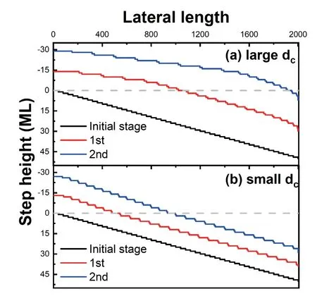
Fig.7.(Color online) The simulated results of morphological change on the trench at a large dc (a) and a small dc (b).The black,red and blue lines denote the morphology at initial stage,after 1st regrowth and after 2nd regrowth,respectively.The steps above the grey dashed lines are new steps from the sidewall.
4.Conclusions
In summary,a new kind of step-flow growth mode applying sidewall as step source is proposed.Terrace width of the steps originated from the etching sidewall can be modified by growth temperature and Ⅴ/Ⅲ ratio.By putting forward a critical terrace width of the step nearest to the sidewall for the creation of new steps,the growth mechanism and relations between the terrace width of new steps and growth conditions are elucidated.The simulated results based on the step motion model show thatdcdirectly determines the terrace width of the steps from the sidewall.These findings provide a deep understanding about step motions of GaN and a novel method of controlling the terrace width that is even applicable to other materials.
Acknowledgments
This work was supported by the National Key Research and Development Program of China (2022YFB2802801),the National Natural Science Foundation of China (61834008,U21A20493),the Key Research and Development Program of Jiangsu Province (BE2020004,BE2021008-1),and the Suzhou Key Laboratory of New-type Laser Display Technology(SZS2022007).
The authors are grateful for the technical support for Nano-X from Suzhou Institute of Nano-Tech and Nano-Bionics,Chinese Academy of Sciences (SINANO).The authors are grateful for the technical support for the Nano Fabrication Facility from Suzhou Institute of Nano-Tech and Nano-Bionics,Chinese Academy of Sciences (SINANO).
杂志排行

Journal of Semiconductors的其它文章
- Efficient flexible dye-sensitized solar cells from rear illumination based on different morphologies of titanium dioxide photoanode
- An advanced theoretical approach to study super-multiperiod superlattices: theory vs experiments
- Two-step growth of β-Ga2O3on c-plane sapphire using MOCVD forsolar-blind photodetector
- Controllable thermal rectification design for buildings based on phase change composites
- Enhanced thermal emission from metal-free,fully epitaxial structures with epsilon-near-zero InAs layers
- Research progress of alkaline earth metal iron-based oxides as anodes for lithium-ion batteries