An advanced theoretical approach to study super-multiperiod superlattices: theory vs experiments
2024-03-02AlexanderSergeevichDashkovSemyonAndreevichKhakhulinDmitriiAlekseevichShapranGennadiiFedorovichGlinskiiNikitaAndreevichKostrominAlexanderLeonidovichVasilievSergeyNikolayevichYakuninOlegSergeevichKomkovEvgeniyViktorovichPirogovMax
Alexander Sergeevich Dashkov ,Semyon Andreevich Khakhulin ,Dmitrii Alekseevich Shapran ,Gennadii Fedorovich Glinskii ,Nikita Andreevich Kostromin,3,Alexander Leonidovich Vasiliev,Sergey Nikolayevich Yakunin,Oleg Sergeevich Komkov,Evgeniy Viktorovich Pirogov,Maxim Sergeevich Sobolev,Leonid Ivanovich Goray,,6,7,and Alexei Dmitrievich Bouravleuv,6,7,8
1Saint-Petersburg Electrotechnical University "LETI",Saint Petersburg,197022,Russian Federation
2Alferov Saint-Petersburg National Research Academic University of the Russian Academy of Sciences,Saint Petersburg,194021,Russian Federation
3Saint Petersburg Polytechnic University of Peter the Great,Saint Petersburg,195251,Russian Federation
4Shubnikov Institute of Crystallography of Federal Scientific Research Centre “Crystallography and Photonics”,Russian Academy of Sciences,Moscow,119333,Russian Federation
5National Research Center ‘Kurchatov Institute’,Moscow,123182,Russian Federation
6University associated with IA EAEC,Saint Petersburg,194044,Russian Federation
7Institute for Analytical Instrumentation,Saint Petersburg,198095,Russian Federation
8Ioffe Institute,Saint Petersburg,194021,Russian Federation
Abstract: A new theoretical method to study super-multiperiod superlattices has been developed.The method combines the precision of the 8-band kp-method with the flexibility of the shooting method and the Monte Carlo approach.This method was applied to examine the finest quality samples of super-multiperiod Al0.3Ga0.7As/GaAs superlattices grown by molecular beam epitaxy.The express photoreflectance spectroscopy method was utilized to validate the proposed theoretical method.For the first time,the accurate theoretical analysis of the energy band diagram of super-multiperiod superlattices with experimental verification has been conducted.The proposed approach highly accurately determines transition peak positions and enables the calculation of the energy band diagram,transition energies,relaxation rates,and gain estimation.It has achieved a remarkably low 5% error compared to the commonly used method,which typically results in a 25% error,and allowed to recover the superlattice parameters.The retrieved intrinsic parameters of the samples aligned with XRD data and growth parameters.The proposed method also accurately predicted the escape of the second energy level for quantum well thicknesses less than 5 nm,as was observed in photoreflectance experiments.The new designs of THz light-emitting devices operating at room temperature were suggested by the developed method.
Key words: super-multiperiod superlattice;photoreflectance spectroscopy;Kane model;kp-method;energy band diagram;light amplifiers
1.Introduction
Semiconductor superlattices (SLs) are semiconductor materials that incorporate a one-dimensional periodic potential with a period larger than the crystal lattice[1].In these materials,the motion of charge carriers is confined along one of the dimensions,resulting in unique quantum properties and modification of the band structure of the host semiconductors.Even several decades after the first study of SL was published,scientific groups still discover new applications[2,3]and curious properties[4,5]of these quantum structures.
One of their most promising applications is the creation of THz-emitting devices.The THz radiation has a variety of essential applications in medicine,astronomy,and telecommunications[6,7],which indicates the need to produce new cutting-edge tunable THz sources operating at room temperature.Multiperiod SLs are the prime candidates for this job because they have all the components required for light amplification and their designs seems to be simpler and more reliable,than designs of quantum cascade lasers (QCLs)[8,9].The ongoing simplification of designs of QCLs towards the SLs[10,11]confirms this conclusion.
Experimental studies and fabrication of SLs have become possible in the last several decades due to significant progress in growth technologies.The most valuable contribution to this research field was made by molecular beam epitaxy (MBE),which brought to life more and more devices with ultra-thin layers.Moreover,a new type of SL,super-multiperiod (SMP) structures,i.e.,SLs with a number of layers from several hundred up to few thousands have been recently implemented by MBE[9,12-16].
In both cases (ordinary or SMP SLs),researchers need to solve the Schrödinger equation with the given periodic electronic potential.The introduction of such potential leads to the transformation of the initial electronic Bloch states and minibands formation.Currently,there are plenty of numerical methods to get this information qualitatively and quantitatively.But they all incorporate a variety of assumptions,limitations,and approximations.For instance,kp-methods consider states in the vicinity of the selected point of the Brillouin zone,whereas the density functional theory calculations require a complex and intense computation procedure[17].At the same time,all these methods are the most appropriate ways to tackle the problem of determination of the electronic properties of SL.However,in more intriguing cases,the theory is yet to be solidified,e.g.,SMP SLs under external electric fields.One of the vivid examples of this fact is the problem of predicted low gain values in SLs[11].It was suggested,that in similar SL structures,the gain is strongly affected by elastic scattering for a higher temperature.To the best of our knowledge,such comprehensive investigations,which considers combination of both experimental and theoretical approaches,have not been conducted yet.
In this work,a new theoretical approach for the modelling of SMP SL parameters is developed.Our method combines theoretical and numerical models,including 8 band kpand shooting methods,as well as Monte Carlo (MC) simulations.The developed approach was proved by the study of the properties of AlxGa1-xAs/GaAs SMP SL samples of the finest quality obtained by MBE.These samples were also examined by the express method of photoreflectance spectroscopy (PRS) and high-resolution transmission electron microscopy (HR TEM).Conducted research establishes the accuracy,applicability,and versatility of the developed approach.
2.Experimental methods and structures
The AlxGa1-xAs/GaAs SMP SLs of high quality were grown on one-sided semi-insulating GaAs (100) substrates using the Riber 49 MBE setup.The reflection high-energy electron diffraction system was used to control the growth processesin situ.The thickness of the GaAs layers in the synthesized SMP SL structures differs across the samples,while the barrier AlxGa1-xAs thickness remains constant.The Al mole fractionxin the barrier layers was equal to 30%.The grown SMP SL structures were doped identically in barriers and wells with silicon as an n-type dopant.All samples had the same concentrations of n-type donor dopant (n=1016cm-3).Table 1 contains all the essential parameters for the samples.

Table 1.Parameters of the AlxGa1-xAs/GaAs superlattices samples under study.
Obtained samples exhibit the excellent quality of the SMP SLs which was confirmed by different methods.The detailed metrology of the grown doped and undoped SMP SL AlxGa1-xAs/GaAs structures with period numbers of 100–400 was carried out by high-resolution X-ray reflectometric (HRXRR),deep X-ray reflectometric (DXRR) and high-resolution diffractometric (HRXRD) studies,in particular,using a synchrotron radiation source[12,13,15,16].The difference in the thicknesses of the grown layers,estimated by three methods and over the entire depth of the optimized SL structures,was no more than 0.5–2.0 percent,the interface root mean square(RMS) roughness was a few Å,and the composition inaccuracy was~0.5 atomic percent.The high sharpness of SLs’ interfaces was also demonstrated by high-resolution transmission electron microscopy (HR TEM) (see Fig.A1 and Supplementary materials)[13,18].
One of the main methods used for precise energy spectrum retrieving was PRS[19,20].PRS is the non-contact,nondestructive,and highly sensitive express method for diagnosing nanostructures.It allowed us to determine the energies of interband optical transitions in nanostructures not only at low[21],but also at room temperature ranges[22,23].One can also obtain information about higher-order optical transitions in different nanostructures[24,25],including type-ⅡSLs[26].The high quality of the grown samples makes this method applicable for the precise examination of optical properties of SMP SLs even at room temperatures.PRS is based on the application of both the probe laser beam,which varies in a wide energy range,and the periodic modulated laser beam.The electron-hole pairs photoinduced as a result of laser exposure are separated by the near-surface built-in electric field.At the frequency of the periodic laser perturbation,a change in the reflectance coefficient is synchronously detected,which underlies the recorded signal[19].During the study of low-dimensional semiconductor structures,the formation of a signal can occur due to a change in the position of quantum-dimensional levels under the action of a change in the built-in electric field due to the Stark effect[27].In case of SLs,the quantum-dimensional levels can be transformed into several energy minibands of finite width.Therefore,singularities in the photoreflectance (PR) spectra can be observed at energies corresponding to the maximum and minimum energies of possible transitions between minibands (near theГandПpoints of the Brillouin zone of the SL)[28-30].
The PR spectra were measured using an experimental setup assembled on the basis of an IKS-31 diffraction spectrometer.The source of modulating radiation was a highly stable SSP-DHS-405 violet laser with an operating wavelength of λ=405 nm.The laser beam was aimed at the exact area of the sample where the spectrometer's monochromatic light was directed to.Modulation signal was recorded using a silicon photodiode,a preamplifier,and a lock-in amplifier (SR830,Stanford Research).The measured PR spectra represent a series of differential signals,the inflection points of which determine the energy values of optical transitions[19].To get accurate energy values and characterize spectral features,PR spectra were transformed using the Kramers–Kronig relations (Kramers–Kronig method,KKM)[31].The Appendix B provides a detailed explanation of this transformation.The extrema of transformed signals determine the precise energy values of the observed optical transitions.
3.Results and discussion
The presented SMP SL structures in Table 1 were initially designed for the light amplifiers’ implementation.The geometry of these SLs was inspired by the structures proposed in Ref.[8] and underwent a few modifications for output characteristics improvement,including estimated gain[9].When the electric field is applied to such SLs,light amplification becomes possible due to the emergence of optical intersubband transitions.Since these transitions occur between energy minibands of SL,their relative position,i.e.,the emitting wavelength,can be tuned with the applied field.In this case,all output characteristics of the SLs depend on their parameters (layer thicknesses,composition,and doping concentrations).For instance,thinner Al0.3Ga0.7As barriers maintain higher dipole matrix element values for optical transitions,resulting in higher gain values.Such qualitative considerations provide a general idea of the structure design but do not define it completely.Therefore,to fully define the structure,i.e.,to choose structure parameters suitable for the task,it is necessary to carry out numerical simulations of the SL energy spectrum.
3.1.Initial design and simulation approaches
The initial designing process was based entirely on the results of the classical shooting method (CSM) simulations[32].Applied CSM utilizes the approximation of the single-bandkp-model,an easily-implementable computation scheme which showed a good agreement with experimental results for a single quantum well,multiple quantum well structures,and ordinary SLs[33,34-37].This method has been also selected because it is frequently utilized to address similar QCL simulation tasks[10,38].CSM retrieves the electronic eigenstates,which define the electronic energy spectrum for a given SL periodic potential.A boundary value problem for the Schrödinger equation in CSM is reduced to the Cauchy problem,i.e.,an initial value problem[32].The electronic eigenstates are determined by 'shooting' solutions from one boundary condition with different initial conditions until the other boundary condition is met.Once the eigenvalues are found,one can employ a transfer matrix approach to retrieve wavefunctions via the propagation procedure.The transition energies are defined as the difference between the values of the corresponding eigenenergies (minibands' boundaries).The electronic energetic spectrum is then utilized in a stochastic MC approach to gather information about the kinetics of the SLs,such as transition rates and gain estimations.The Fermi golden rule is applied to calculate the scattering rates used in MC,including phonon and impurity scattering rates.For example,to calculate the impurity scattering rate the following formula can be employed:
To estimate gain based on dipole matrix elementDand doping concentratingne,the following formula,obtained from two level model was used[32]:
whereDulis the dipole matrix element for transition between upper and lower levels,τulis the inverse transition rate between upper and lower levels.
During the design phase,we varied the thicknesses of all the layers and layer composition to maximize both the figure of merit and gain estimation while preserving the emitting wavelength in the THz range.In order to check the calculated design,a series of SMP SL Al0.3Ga0.7As/GaAs structures were grown (Table 1).SMP SL structures had sharp interfaces,their thicknesses and composition deviations were minimal(see Fig.A1 and Supplementary materials).The creation of such high-quality SMP SLs with required layer thicknesses and acceptable interface widths became possible due to laboratory and synchrotron studies[12],as it was mentioned in the previous section.
The optical properties of the samples were examined by PRS to determine the electronic energy spectrum.The PR examination is a suitable verification tool because the electronic energy spectrum and the optical output features of the structures are closely interconnected.Therefore,for all the grown SMP SL structures,PR spectra were measured and transformed according to the method described in the previous section and Supplementary materials.The data obtained were compared with CSM results.For instance,the e1-hh1 transition energy,i.e.,the difference between the first electronic(e1) and the first heavy hole (hh1) energy levels,was compared with the position of the first peak in the transformed spectrum.
We anticipated only minor deviations between experimental and simulated values since CSM is widely applied in similar QCL design tasks[32].However,the PR analysis (Fig.1) of sample no.1 showed a significant deviation from the expected band structure: simulated energy values (green arrows in Fig.1) and experimental values (black dotted arrows in Fig.1) differed for e1-hh1 and e1-lh1 transitions by 15 meV and 23 meV,respectively.That results in a total error of about 25% and makes CSM inapplicable for the proper and complete electronic energy spectra analysis of SMP SLs.

Fig.1.(Color online) The transformed PR spectrum of sample no.1 measured at T=300 K.Black dotted arrows indicate the experimental transition energy peaks and green solid arrows indicate the transition energy positions computed by CSM.
As CSM was not suitable for the analysis of the transformed PR spectrum,we had to find an alternative simulation approach.The first idea was to test more advanced purely numerical methods: the finite elements method (FEM),which numerically solves the Schrödinger equation for an infinite SL on the specified grid[32];the transfer matrix approach with the Airy functions and immense modifications of the shooting method,which also provides the numerical procedure to obtain the minibands position of SL[32,37].We reduced the error to 10%,but the accuracy of these methods was still insufficient for an unambiguous analysis of experimental data.Therefore,we changed our simulation approach to a more elaborate one.
It is well known that the theoretical study of semiconductor heterostructures and SLs can be done in various ways: the empirical pseudopotential method (EPM)[33,45-48],the tight binding (TB) method[33,48],and thekp-method[33-36].All of the mentioned methods allow to simulate SLs with a large number of periods (here,SMP SLs).However,there are few works only[8,11]that include the experimental study of such SLs combined with theoretical and numerical analysis.Some of these methods even assume that the SL under consideration is infinite[33-36,46-52].This is also an approximation to be verified with the experimental data.Taking into account all of these facts,it was not clear which method to choose.The EPM has an advantage over TB,since EPM requires fewer adjustable parameters and a suitable basis for the solving of the Schrödinger equation can always be chosen.The EPM makes it possible to obtain results those are in good agreement with the experiment[33,45,46],since it can account any number of bands contributing to the formation of energy states.However,such many band EPM considerations impose additional computational requirements even for the structures whose dimensions are just a few nanometers.Although there are ways to get around these difficulties[33],the computers used have not allowed one to study SMP SLs with a supercell of more than~2–3 nm in size by this method.Thekpmethod is suitable for investigation of nanostructures larger than a few nanometers,including SMP SLs,as it was demonstrated in Refs.[36,50].This method is also among the most appropriate methods for analyzing experimental data.The complexity of thekp-method increases with the number of bands considered in the calculation[34-36,53].The initial simulation approach included only an approximation of the single bandkp-method,which probably was the reason for poor accuracy.Thus,we selected the below-described 8-bandkpmethod,also known as the Kane model,for the appropriate theoretical study of the SMP SLs.
3.2.Theoretical study of SMP SLs: the Kane model
The 8-band Kane model was previously used to calculate the energy spectrum and interband matrix elements of similar heterostructures and SLs[49].One of the key advantages of the Kane model is that it allows to consider the nonparabolicity of the charge carriers' dispersion law.Another bonus is the insignificant computational burden of the model,even in our case of SMP SLs[35].The model can be formulated as an eigenenergy problem for the Schrödinger equation with the following Hamiltonian:
According to Refs.[35,49],this Hamiltonian matrix includes the effective Hamiltonians,where k,k′are the wave vector of an electron in the Brillouin zone of the crystal,α,α′are the indexes of the considered bands (are the centers of the Brillouin zone of a bulk crystal for the conduction,valence,and spin-split bands,respectively,with spin momentum projections(c=±1/2),(v=±3/2,±1/2) and(v=±1/2),K is the wave vector of an electron in the Brillouin zone of SL.The main diagonal elements are the one-band effective Hamiltonians,and the off-diagonal elements describe the effects of the interbandkp-interaction.Both types of Hamiltonians include the difference in the interband parameters of the materials when passing through the interface.When solving this problem,one can prevent false solutions in the multiband model by the k–representation method since the considered region of k–space can be limited based on the estimated width of the wave functions compared to the size of the Brillouin zone.
The primary method to solve the Schrödinger equation involved a periodical continuation of a single quantum well[35,51,52].The periodicity condition leads to the fact that the wave vector k of an electron in a crystal becomes discrete,and the Schrödinger equation itself turns into a system of algebraic equations
To interpret the experimental data presented in Fig.1,the calculation of the energy spectrum of charge carriers by Eq.(6) is not enough,since the experimental data reflect only the optical transition probabilities.The optical transition probabilities can be obtained from analyses of interband matrix elements,which are calculated with the following formula(neglecting thekp-interaction of electrons and holes):
where Pcvis the matrix element of the momentum operator.For transitions of charge carriers from the valence bandto the conduction bandFor transitions from the spin-split bandto the conduction bandits projections have the form
For the energy spectrum of charge carriers and interband matrix elements calculations the parameters of initial materials from Table 2 were used[54].The Kane parameters required for the calculation were determined through the constants presented in Table 2 as follows:

Table 2.The band structure parameters used in the Kane model calculations at T=300 K.
wherem0is the electron mass.
The band offset parameters were obtained from Ref.[50]and corresponded to the following relationship ΔEc/ΔEv=0.67/0.33.The band offset of spin-split bands was defined asIt was also assumed that neglected deformation effects are insignificant since the relative difference between the constant lattices of the well and barrier materials is ∣ε⊥∣=0.097%.Therefore,the lattice period in the superlattice was taken as the AlxGa1-xAs period.We computed the transition energies for considered SMP SL structures using the above-described formulae.The resulting values are demonstrated in Table 3 and they were used for further PR spectra analysis.

Table 3.Values of the optical transition energies (eV) calculated with the Kane model.
3.3.Theoretical calculations results vs experimental spectra
The above-mentioned results can be also illustrated as the electronic minibands in the conduction band in Fig.2.Figs.2(a) and 2(b) show the relevantE(K) dependences for the electronic states,whereKvaries within the Brillouin zone of the SL ((Kz≠0,Kx,Ky=0)).The sizes along thez-dimension of the unit cell of the SLs in the model areD=12.4 andD=9.05 nm,respectively.From these figures,one can conclude that the third electronic subband e3 for SL no.1 is partially localized within the well.As a result,its PR spectrum has optical transitions involving e3 not only at pointГbut also at pointП(edge of Brillouin zone of the SL) with above-barrier energy levels (see Fig.2(c)).

Fig.2.(Color online) The electronic energy-band structure calculated by Kane model corresponding to sample no.1 and 2 from Table 1.(a)Electronic energy-band structure of the SMP SL no.1.(b) Electronic energy-band structure of the SMP SL no.2.(c) Electronic subband energies and bandwidth of the SMP SL no.1.(d) Electronic subband energies and bandwidth of the SMP SL no.2.
Within the scope of the considered,it was assumed that the profile of quantum wells in the superlattice is rectangular (trapezoidal–under electric fields) with abrupt interfaces.The distortions of the conduction/valence bands profiles were neglected due to the insignificant magnitude for the considered doping concentrations.The presence of sharp interfaces was shown by the results of HR HAADF STEM,HRXRR,DXRR,HRXRD investigations.To compensate the minor distortions of the potential profile,the size of a single SL period for the first sample (with period 12 nm) was increased by one GaAs monolayer to obtain better convergence.
Electronic energy spectra calculated by the Kane model(Table 3,Fig.2) were consistent with transformed PR spectra of the synthesized Al0.3Ga0.7As/GaAs SMP SLs (Fig.3).The comparison between experimental and theoretical data allowed us to interpret transformed PR spectra in detail.All the simulated transitions are presented on obtained spectra in Fig.3 with colored solid arrows.The small broadening of spectral lines shown in Fig.3(a) confirms the high quality of SMP SL samples.The most intensive and narrow spectral line at 1.449 eV corresponds to the main optical interband transition e1-hh1 at theГpoint (center of the Brillouin zone of the SL).The next less intensive peak at 1.461 eV corresponds to the e1-lh1 transition at theГpoint.The high quality of the SL has led to a small broadening of spectral lines and these two peaks with extrema position difference of 12 meV turned out to be resolved even at room temperature.Their position,as well as the position of other marked peaks,is in good agreement with the Kane model calculations.

Fig.3.(Color online) Transformed PR spectra of samples no.1 (a) and no.2 (b) from Table 1 measured at T=300 K.
Fig.3 also compares the transformed PR spectra of the superlattices samples no.1 (Fig.3(a)) and no.2 (Fig.3(b))with periodsD=12.0 nm and 8.99 nm,respectively.A decrease in the superlattice period from 12.0 to 9 nm led to a significant increase in the same optical transition energies observed in the spectrum (Fig.3(b)).The main optical transition in sample no.2 increased in energy up to 1.483 eV.The left shoulder of the main optical transition peak in the transformed spectrum is assumed to be associated with the impurity exciton state.According to Kane model calculations with such SL configuration,two electron subbands are formed,while the second subband is only partially localized within the well (see Fig.2(c)).As a result,relatively intense transitions are observed in the spectrum with the participation of the e2 subband at theПpoint around 1.63-1.68 eV and less intense transitions at theГpoint with above-barrier transitions.
The difference between experimentally obtained and computed transition energies does not exceed several meV.The proposed Kane model allowed us to significantly reduce the error of the peak positions from 25% to 1%-5%.Also,using the Kane model,it became possible to obtain the precise position of minibands in the range of SL designs (Fig.4).Obtained results show smooth dependence from the width of the well.It is also worth mentioning that there is a threshold width value of 5 nm.For more narrow quantum wells,the expectation is that the second eigenstate won’t be observable in PR analysis.
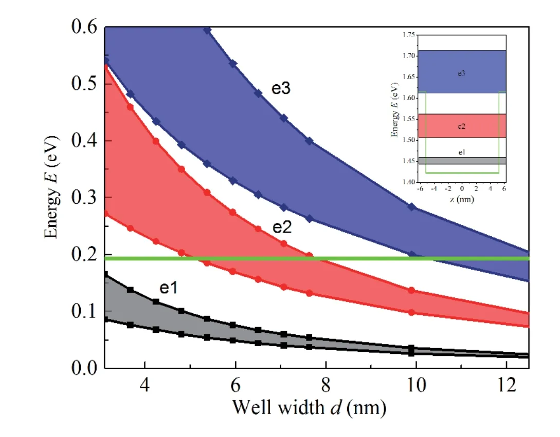
Fig.4.(Color online) Electronic subband energies and bandwidth calculated by the Kane model as a function of well thickness,with a fixed barrier thickness of 2 nm.The energy zero coincides with the GaAs conduction band edge.The graph exhibits the positions for both Γ andΠ point in the Brillouin zone of the SLs.The solid light green horizontal line represents the position of the Al0.3Ga0.7As (barrier layers) conduction band edge.The inset contains the energy-band diagram demonstrated in Fig.2(c).
The Kane model described above is highly accurate,but it can simulate the band diagram and electronic energy spectrum only.This model is not intended to calculate electronic transition rates between corresponding energy states.Therefore,other methods,that consider electronic transitions,should be used to estimate scattering rates and gain.Since CSM,described earlier,can calculate these characteristics,we decided to combine the 8-bandkp-model with the “shooting approach”.The simulation process of our method can be divided into the following steps:
(1) initially,energy level positions (their vicinity),effective masses,theoretical period of SL,etc.were computed with the Kane model;
(2) computed parameters were fed to CSM to obtain the accurate solution of the Schrödinger equation,i.e.,the eigenvalues and eigenvectors for the given Hamiltonian;
(3) the figures of merit,transition rates,and gain estimates were calculated by MC approach and Eqs.(1)-(4) with eigenvalues and eigenvectors,obtained in the previous step.This sequence of steps preserves the accuracy of the Kane model and allows to estimate gain.Thus,this method has all the prerequisites to become a new and more reliable alternative to commonly used approaches.
To get the highest gain estimate and maintain the frequency of amplified light in the THz range,we have varied the thickness of the quantum well between 7 and 10 nm.The results obtained by our new method are presented in Fig.5-Fig.7.All of the below-mentioned computations were performed for the temperature of 300 K.Fig.5 demonstrates the frequency dependence of the estimated gain for different quantum well thicknesses.The graph illustrates that wider quantum wells provide higher gain values,but the radiation frequency is blue-shifted towards 2.5 THz.Presumably,the higher gain values are achieved due to the increased wave function localization in wider wells.

Fig.5.(Color online) Simulated gain vs.radiation frequency for SMP SL with quantum well thicknesses between 7 and 10 nm and a fixed barrier thickness of 2 nm.
Fig.6 shows the figure of merit dependence on the quantum well thickness.The plot confirms that wider quantum wells result in higher gain,as shown by the figure of merit dependence on quantum well width.According to this graph,the most suitable width values,where the highestFMcan be obtained,are between 8.5 and 9.5 nm.The maximum position is expected to be at 8.8 nm.

Fig.6.The computed figure of merit values vs.quantum well width for SLs with a fixed barrier thickness of 2 nm.
Scattering rates for LO-phonon and impurity mechanisms were also calculated during simulations,and their dependency on quantum well width is shown in Fig.7.Shorter scattering times result in faster depopulation of the level,i.e.,designs with longer scattering times for the upper level and shorter times for the lower level are the most convenient for the population inversion maintenance.Therefore,the most suitable region in Fig.7 is between 8.5 and 10 nm:

Fig.7.(Color online) Simulated scattering times of upper and lower level for two mechanisms: LO-phonon (LO),impurity scattering (imp)vs.quantum well width for SLs with a fixed barrier thickness of 2 nm.
• scattering times for the lower level at their minima(they do not exceed 1.5 ps);
• scattering times for the upper level are relatively high(approximately 5 ps).To summarize all the mentioned results,the most promising structure for a THz source implementation is a considered SMP SL with an 8.5 nm thick quantum well.This geometry provides a higher gain estimate and allows to maintain population inversion with small broadening valuesγ.
The described combination of PR and Kane model can be used in a more self-contained manner.To show that,the authors also enhanced this method with the process of naïve optimization,where all the following ranges of SL parameters are brute-forced: mole fraction of Al in barrier layers between 10% and 40%,well thickness from 4 to 15 nm.Achieved minimum deviation met expectations,and its position was in good agreement with XRD data and growth parameters.By changing the thickness of the well,one can also control the number of eigenstates inside the SL.As was previously shown,wider quantum wells contain a third undesirable energy level[9].The proposed method predicted the escape of the second energy level when reducing quantum well thickness,which is illustrated in Fig.2.
To minimize the adverse impact of elastic scattering,it is suggested to increase the number of periods and decrease the doping concentration of the layers.According to the estimations (Fig.5),this must significantly decrease (down to several magnitudes) the influence of the elastic scattering,while maintaining high gain values.With the above-described adjusted energy values from the Kane model,the dipole matrix element,relaxation times,and the estimation of the gain coefficient were calculated (Fig.5-Fig.7).Obtained values showed a gain slightly above 40 cm-1for the proposed SL with a quantum well layer thickness of 8 nm.We assume that the gain values (see Fig.5) are significant enough to produce light emission,as the total expected losses are estimated to be below 15 cm-1.To estimate the waveguide loss,we considered the double metal waveguide from Ref.[55].It should be also mentioned that this structure is the best for light amplification due to the electron transport estimations that exhibit a positive differential conductivity region near the operating point[9,11].
4.Conclusion
In conclusion,this paper presents the first and unique comprehensive theoretical analysis of the energy band diagram for super-multiperiod superlattices,verified by experimental data.The authors have developed a new combined method for the theoretical study of multiperiod superlattices.It fuses the precision of the Kane model and the flexibility of the shooting method with the Monte Carlo technique,which results in a more refined and versatile approach.This method was applied to analyze state-of-the-art samples of super-multiperiod superlattices grown by molecular beam epitaxy.The express room-temperature method of photoreflectance was used for experimental approbation.The proposed method diminished the error in the identification of the transition energy peaks to just 5%,presenting a substantial improvement compared to the typical 25% error obtained with conventional approaches.The photoreflectance experiments validated the accuracy and reliability of the combined method.The approach successfully predicted the escape of the second energy level in structures with quantum well thicknesses below 5 nm.The authors reinforced the method with naïve optimization to restore the intrinsic superlattice parameters.The recovered parameters correlated well with X-ray diffractometric data and growth parameters.
The refined method is also suitable for calculating transition rates and estimating gain.Therefore,it was used to design a new light-amplifying super-multiperiod superlattice.Additionally,the authors revealed ways to reduce the impact of elastic scattering in these constructions.The scheme developed in the research boosts the creation of both efficient light amplification and adjustable sources of terahertz and infrared radiation.
Acknowledgements
The work was supported by the Ministry of Education and Science of the Russian Federation in the framework of experimental research (Nos.075-01438-22-06 and FSEE-2022-0018) and the Russian Science Foundation in theoretical research (No.RSF 23-29-00216).
Appendixes A and B.Supplementary materials
Supplementary materials to this article can be found online at https://doi.org/10.1088/1674-4926/45/2/022701.
杂志排行

Journal of Semiconductors的其它文章
- Efficient flexible dye-sensitized solar cells from rear illumination based on different morphologies of titanium dioxide photoanode
- Two-step growth of β-Ga2O3on c-plane sapphire using MOCVD forsolar-blind photodetector
- Controllable step-flow growth of GaN on patterned freestanding substrate
- Controllable thermal rectification design for buildings based on phase change composites
- Enhanced thermal emission from metal-free,fully epitaxial structures with epsilon-near-zero InAs layers
- Research progress of alkaline earth metal iron-based oxides as anodes for lithium-ion batteries