金刚石薄膜在第一壁材料表面的应力研究
2022-11-08耿传文赵鹏张晓东曾梅花MiroljubVilotijevic
耿传文,赵鹏,张晓东,曾梅花,Miroljub Vilotijevic
金刚石薄膜在第一壁材料表面的应力研究
耿传文1,2,赵鹏1,张晓东1,曾梅花1,Miroljub Vilotijevic1
(1.中国科学院合肥物质科学研究院,安徽 合肥 230031;2.中国科学技术大学,安徽 合肥 230026)
提出在第一壁材料(钨穿管部件)表面沉积金刚石薄膜,并系统研究金刚石薄膜厚度对应力的影响。采用数值模拟和实验表征方法。利用ANSYS workbench模拟软件,在建立钨穿管部件表面金刚石薄膜有限元模型及模型方程的基础上,对影响金刚石薄膜热残余应力的厚度因素进行探讨;采用微波等离子体化学气相沉积法(MPCVD),在钨穿管部件表面沉积不同厚度的金刚石薄膜,并利用拉曼光谱法和洛氏硬度计压痕法对薄膜的应力进行表征。模拟显示,随着金刚石薄膜厚度增加,薄膜最大主应力值和最大剪应力值均呈现出先减少后增加趋势,在薄膜厚度为75~100 μm时处于最低,小于金刚石薄膜通常的断裂强度(700 MPa),同时最大应力落差区域出现在薄膜边缘处。通过实验表征得到金刚石薄膜表面呈现出拉应力,在薄膜厚度为(103.56±0.5)μm时,金刚石薄膜中间区域应力值最低,与VDI3198标准对比,压痕坑达到HF1和HF2效果。钨穿管部件表面金刚石薄膜厚度为(103.56±0.5)μm时,不容易出现裂纹和与基底的剥离现象,具有较好的附着性。
金刚石薄膜;第一壁材料;应力;等离子体;钨穿管部件
核聚变能是解决人类能源问题的重要途径,利用磁约束热核聚变反应装置(托卡马克,TOKAMAK)是最有希望实现聚变能发电的装置[1-2]。在托卡马克装置中,第一壁材料(穿管部件)由于直接面向高温等离子体并与之相互作用(PMI),使得材料需要经受超500 ℃的高温、10 MW/m2的高热通量、14 MeV的高强度中子辐照等极端服役环境,不仅轰击产生的杂质造成聚变堆能量损失,还会引起材料自身辐照损伤、热腐蚀和溅射腐蚀[3-5]。钨和碳基材料(石墨、碳纤维复合材料)是目前被认为第一壁材料最理想的2种材料,已经广泛应用于世界上大多数托卡马克装置中[6-7]。但钨是高原子序数材料,在等离子体高约束模式运行条件下容易聚芯,影响高温等离子体稳定运行[8],而石墨与碳纤维复合材料由于高溅射产额也难以满足第一壁材料的要求[9]。金刚石最密排的结构使其成为自然界硬度最高和导热性能最好的材料,同时具有良好的抗物理溅射及化学腐蚀的性能,耐热冲击性好,且可以抑制氢同位素的渗透,这些已经在聚变堆中得到认证[10-13]。目前,制备金刚石最常见的方法为化学气相沉积法(CVD),而对比热丝法(HFCVD)、直流法(DCPCVD)、燃烧火焰法(CFCVD)等方法,微波法(MPCVD)采用无极放电,所制备的材料杂质低、纯度高,在托卡马克装置应用中具有更大优势。使用MPCVD方法在钨穿管部件的面对等离子体方向表面制备金刚石薄膜,有望成为第一壁材料的新选择。
在金刚石薄膜制备过程中不可避免会有应力产生,应力的大小及分布直接决定薄膜的性能与使用稳定性。应力又可分为本征应力与热残余应力,本征应力主要与在制备过程中杂质的引入及自身的结构特征有关,热残余应力由于受薄膜与基底热膨胀系数不匹配和薄膜厚度的影响,使得在高温制备完毕后的冷却过程中产生不均匀塑性变形。在MPCVD法制备金刚石薄膜中,热残余应力的影响往往远大于本征应力,这是导致金刚石薄膜产生开裂破坏、与基底剥离等现象的主要因素[14-15]。而目前对于热残余应力的研究途径大多集中在采用基片曲率法[16]和XRD[17]等方法,这些方法受限于基底或者薄膜厚度的影响,难以得到薄膜冷却过程中热残余应力的瞬态变化。为此,首先采用有限元软件ANSYS workbench对钨表面金刚石薄膜的热残余应力进行模拟,研究膜厚对热残余应力大小及分布的影响,确定金刚石薄膜的最佳沉积厚度范围;其次,使用MPCVD法在钨穿管部件表面制备与模拟结果厚度相匹配的金刚石薄膜,通过拉曼光谱法和压痕法研究薄膜厚度对其总应力和与基底附着力大小的影响。
1 有限元分析膜厚对金刚石薄膜热残余应力的影响
薄膜厚度是影响热残余应力最主要的因素之一[18-19],采用ANSYS workbench软件对钨穿管部件表面厚度为25~300 μm的金刚石薄膜进行模拟,研究厚度对薄膜残余应力大小及分布的影响,对膜内危险位置和失效方式进行初步分析,为金刚石薄膜的最佳制备参数的选择提供依据。
1.1 研究方法
1.1.1 模型建立及假设
钨穿管部件(××, 26 mm×13 mm×26 mm)及金刚石薄膜有限元网格模型见图1,网格采用自由划分方式(见图1a),同时为了模拟的准确性,对薄膜及周围区域进行局部网格加密(见图1b)。冷却方式设置为钨穿管部件底部固定水冷,对流传热系数根据实验结果设定为500 W/(m2·K)。钨穿管部件及金刚石薄膜初始温度均设置为800 ℃,这也是最适合金刚石薄膜生长的温度[20],冷却后的温度为22 ℃。材料性能参数设置为:金刚石和钨的弹性模量分别为1 000 GPa和410 GPa,泊松比分别为0.07和0.28,考虑到热膨胀系数随温度的改变而变化,取值参考GA slack等[21]的研究结果。
模型假设:
1)金刚石薄膜与钨穿管部件表面之间无外力和缺陷影响。
2)金刚石薄膜初始状态处于均匀温度且无应力状态。
3)金刚石薄膜与钨基底物理性质为各向同性。
4)MPCVD腔体内为低气压与低气体流量,不考虑气体热传导对结果的影响。
5)金刚石薄膜的厚度远小于其他两个方向尺度,
故把金刚石薄膜视为表面平整模型。
1.1.2 模型方程
热传导的三维瞬态温度场公式见式(1)—(2)[22]。
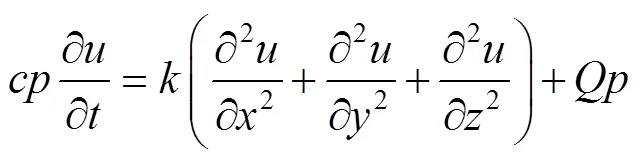
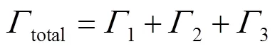
1,2,3三者的边界条件分别见式(3)—(5)。
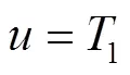


式(1)—(5)中:为比热容;为材料密度;为热扩散率;是在(,,,)的场变量;为热源密度;为物体的边界,1为1边界温度;为各方向外法线余弦;为定流热量;为换热系数;2为环境温度。
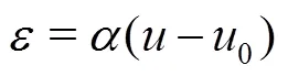
热应力中的热应变是由温度引起[22],公式见式(6)。
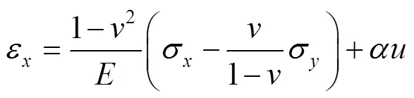
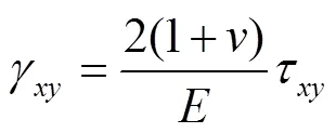
考虑到薄膜与基底之间的相互约束,其场变量的形变分量见式(7)—(9)。

在薄膜某一点的总形变分量见式(10)—(11)。
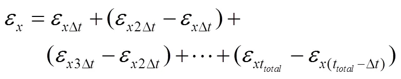
式(6)—(11)中:为弹性模量;为正应变;为正应力;为剪切应变;为剪切应力;为比例系数
图1 钨穿管部件及金刚石薄膜有限元网格模型
1.2 模拟结果与讨论
由于金刚石薄膜属于脆性材料,采用第一强度理论,最大主应力(1)是金刚石薄膜破坏的主要因素[23]。在不改变其他参数的前提下,仅改变金刚石薄膜的厚度,不同厚度下金刚石薄膜整体、上表面和与基底接触底面三者区域中1最高值(max)的变化趋势见图2,可以看出max均呈现出先降低后上升的趋势。当厚度为25~35 μm时,由于金刚石薄膜较薄,三者区域中1具有相近的max值;在厚度为75 μm时,三者区域中1的max均达到最低值,且薄膜上表面的max低于其他区域。随着薄膜厚度的继续增加,max也随之上升,同时max的最小值逐渐由金刚石薄膜的上表面转移到与基底的接触面。由于金刚石具有较高的导热率,当厚度较薄时,金刚石薄膜具有均匀的温度分布与变化趋势,产生的应力无差异;随着薄膜厚度的增加,由于金刚石和钨的热膨胀系数与导热率的差异,薄膜不同部位的温度下降逐渐具有差异性,表面下降的变化速率最快,应力增长的趋势也相应最快。与此同时,5~100 μm厚度的max小于700 MPa,低于金刚石薄膜通常的断裂强度范围[24],避免了热残余应力引起的薄膜断裂现象。
图3所示为厚度75 μm的金刚石薄膜上表面的1分布。从图3可以看出,金刚石薄膜表面1以拉应力为主,仅仅在角落处为压应力,且整个表面的1最高值与最低值都集中在角落处,可以看出,钨穿管部件表面的金刚石薄膜在降温时的角落处可能最容易产生破裂。
图2 金刚石薄膜各部位最大主应力σmax随厚度变化趋势
图3 厚度75 μm的金刚石薄膜上表面σ1分布
薄膜与基体之间的剪切应力是薄膜剥落的主要原因,图4所示为不同厚度下金刚石薄膜整体、上表面和与基底接触底面三者最大剪切应力的最高值(max)变化趋势。从图4可以看出,max变化趋势和max相同,呈现出先降低后上升的趋势,且在薄膜厚度为100 μm时最低,位于金刚石薄膜与基底接触底面,有利于金刚石薄膜在钨上的附着。结合max模拟数据,当膜厚为75~100 μm时,钨穿管部件表面的金刚石薄膜适合在第一壁材料上应用。
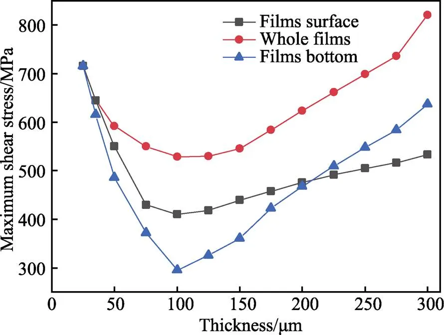
图4 金刚石薄膜各部位最大剪切应力τmax随厚度变化趋势
2 膜厚对钨穿管部件表面金刚石薄膜应力影响的实验研究
高性能的第一壁材料对聚变堆运行尤为重要。有限元模拟结果得到具有低热残余应力值的金刚石薄膜厚度范围,通过MPCVD法在钨穿管部件表面制备与模拟结果厚度相匹配的金刚石薄膜,对薄膜总的应力大小及与基底附着力的表征,是考察金刚石薄膜在第一壁材料表面能否实际应用的关键所在。
2.1 样品制备及测试
采用双基片台压缩波导式MPCVD装置制备金刚石薄膜(见图5),其工作频率为2.45 GHz,最大输出功率3 kW,工作中可产生高密度的等离子体[25],同时等离子体可以均匀覆盖钨穿管部件表面,可高效地制备金刚石薄膜[26]。螺旋测微仪用于测量金刚石薄膜厚度。将反复用酒精超声清理后的钨穿管部件放入微波腔体,通入甲烷(纯度为99.9999%)与氢气(纯度为99.999%),微波激发产生等离子体。甲烷提供金刚石生长的碳源,氢气可以激发甲烷和刻蚀生成的石墨相,减少本征应力。其反应公式见式(12)—(15)。


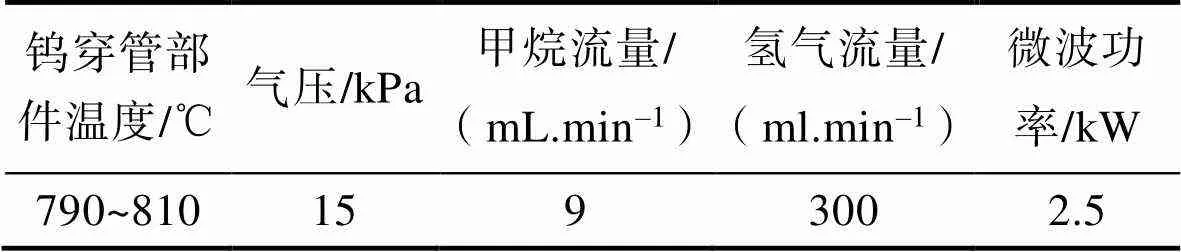
在钨穿管部件表面分别经过8、9.5、11、12 h化学气相沉积,沉积参数见表1,得到厚度分别为(55.48± 0.5)、(80.86±0.5)、(103.56±0.5)、(123.84±0.5)μm等4个金刚石薄膜,沉积后金刚石薄膜照片如图5b所示。采用532 nm激发波长的显微共焦拉曼光谱仪(LabRAM HR Evolution)对金刚石薄膜的应力进行测试与分析,应力大小计算公式见式(16)[27]。

式中:为测试位置的拉曼峰位;0为金刚石标准一阶拉曼峰位(1 332 cm–1);= –0.567 GPa/cm–1。
同时,采用洛氏硬度计压痕法与VDI3198标准对比研究,对样品基底和金刚石薄膜之间的结合性能进行表征,压痕载荷为1 470 N,每次加载时间为15 s。
表1 MPCVD制备样品实验参数
Tab.1 Experimental parameters of samples prepared by MPCVD
2.2 表征结果与讨论
图6为不同厚度金刚石薄膜表面4个采集点位置的Raman峰值,采集点位置如图5b所示。与标准金刚石一阶特征峰1 332 cm–1比较可以看出,所有采集点Raman峰位均向低波段偏移,呈现出拉应力。其中,膜厚为(103.56±0.5)μm的金刚石薄膜Raman峰位偏移最小,具有最小的拉应力。一般认为,CVD金刚石薄膜的晶界处产生拉应力[28]。在金刚石异质外延生长初始阶段,含碳前驱物形成三维岛状晶核单独生长,然后彼此连接形成大量晶界,增加了薄膜的本征应力[29-31]。随着含碳前驱物继续沉积,金刚石晶粒体积增大并相互合并,晶界数量的降低使得薄膜本征应力得到缓解[32-33]。之后薄膜厚度持续增加,晶粒合并得到制约转为纵向生长[34],热残余应力在总应力中占据绝对地位,结合前述的模拟结果,随着薄膜厚度的继续增加总应力随之增大。同时,在膜厚为(103.56± 0.5)μm的金刚石薄膜4个采集点的Raman峰位中,薄膜正中间区域的Raman峰位为1 331.75 cm–1,更接近1 332 cm–1,将其代入Raman应力公式(12)中,得到拉应力为141.75 MPa,而相应边角处拉应力最大为635.04 MPa。因此,边角处过高的拉应力会导致裂纹的出现。
洛氏硬度计对材料处理后的压痕坑可以反映薄膜性能及与基底之间的附着力[28]。将4个厚度的金刚石薄膜的4号采集点位置进行洛氏硬度计压痕,压痕坑见图7。由图7a可以看出,厚度为(55.48±0.5)μm的金刚石薄膜压痕坑边缘出现不规则破损和与基底之间的剥离痕迹;由图7b可以看出,厚度为(80.86±0.5)μm的金刚石薄膜压痕坑完整性优于图7a;由图7c可以看出,厚度为(103.56±0.5)μm的金刚石薄膜与图7d厚度为(123.84±0.5)μm的金刚石薄膜的压痕坑呈现出几乎标准圆形图案,表明薄膜性能最好,完全没有剥离迹象。可见,压痕测试结果与Raman光谱表征结果相互验证,厚度为(103.56±0.5)μm的金刚石薄膜不容易被损坏,体现出最好的性能。将图7c与VDI3198标准进行对照,可以得到压痕坑达到HF1和HF2等级,说明(103.56± 0.5)μm厚度金刚石薄膜与基底具有较高的附着力。

图5 双基片台压缩波导式MPCVD装置制备金刚石薄膜

图6 不同厚度金刚石薄膜4个采集点位置的Raman峰位

图7 不同厚度下金刚石薄膜表面4号采集点位置的洛氏压痕坑SEM图
3 结论
提出在钨穿管部件表面制备金刚石薄膜的技术方案,可作为托卡马克装置第一壁材料的选择。采用ANSYS workbench模拟软件,对不同厚度金刚石薄膜制备完成后冷却产生的热残余应力进行有限元模拟,结果表明:随着金刚石膜厚的增加,金刚石薄膜整体的max与max呈现出先降低后上升的趋势,最低值在膜厚为75~100 μm处,同时,薄膜边角处具有应力较大的变化趋势,容易出现破裂现象;使用MPCVD法在钨穿管部件表面分别制备出厚度为(55.48±0.5)、(80.86±0.5)、(103.56±0.5)、(123.84±0.5)μm等4个金刚石薄膜,通过拉曼光谱法及洛氏硬度计压痕法对比研究发现,(103.56±0.5)μm厚度的金刚石薄膜具有最小的总应力及与基底最好的附着性,满足托卡马克装置第一壁材料的应力要求最好。
[1] Venema L, Verberck B, Georgescu I, et al. The quasiparticle zoo[J]. Nature Physics, 2016, 12(12): 1085- 1089.
[2] Budnitz R J. Nuclear power: Status report and future prospects[J]. Energy Policy, 2016, 96: 735-739.
[3] Spilker B, Linke J, Pintsuk G, et al. Impact of the surface quality on the thermal shock performance of beryllium armor tiles for first wall applications[J]. Fusion Engineering & Design, 2016, 109/110/111(PT.b): 1692- 1696.
[4] Fan H, Tao S, Wu Z. Morphology and crystalline evolution of tungsten induced by low-energy helium ions irradiation[J]. Journal of Radioanalytical and Nuclear Chemistry, 2019, 319, 75-81.
[5] Joffrin E, Pau A. Overview of the JET preparation for Deuterium-Tritium Operation with the ITER Like-Wall [J]. Nuclear fusion, 2019, 59(11): 112021.
[6] Lemahieu N, Greuner H, Linke J, et al. Synergistic effects of ELMs and steady state H and H/He irradiation on tungsten[J]. Fusion Engineering and Design, 2015, 98/99: 2020-2024.
[7] Roth J, Tsitrone E, Loarer T, et al. Tritium inventory in ITER plasma-facing materials and tritium removalprocedures[J]. Plasma Physics & Controlled Fusion, 2008, 50(10): 103001.
[8] Sun F, Nakata M, Lee S E, et al. Synergistic effects of high energy helium irradiation and damage introduction at high temperature on hydrogen isotope retention in plasma facing materials[J]. Journal of Nuclear Materials, 2020, 533: 152122.
[9] 龙海川, 邱长军, 郑鹏飞, 等. 面向等离子体壁材料的腐蚀行为与涂层防护综述[J]. 表面技术, 2021, 50(2): 123-133.
LONG Hai-chuan,QIU Chang-jun,ZHENG Peng-fei, et al. Review on the corrosion behavior and coating protection of plasma facing materials[J]. Surface Technology, 2021, 50(2): 123-133.
[10] Deslandes A, Guenette M C, Corr C S, et al. Deuterium retention and near-surface modification of ion-irradiated diamond exposed to fusion-relevant plasma[J]. Nuclear Fusion, 2014, 54(7): 073003.
[11] Guenette M C, Deslandes A, Thomsen L, et al. D and D/He plasma interactions with diamond: Surface modification and D retention[J]. Diamond & Related Materials, 2014, 49: 103-110.
[12] Porro S, Temmerman G D, Lisgo S, et al. Nanocrystalline diamond coating of fusion plasma facing components[J]. Diamond & Related Materials, 2009, 18(5): 740-744.
[13] Dunn A R, Duffy D M, Stoneham A M. A molecular dynamics study of diamond exposed to tritium bombardment for fusion applications[J]. Nuclear Inst & Methods in Physics Research B, 2011, 269(14): 1724-1726.
[14] Liu J, Wang Y, Costil S, et al. Numerical and experimental analysis of molten pool dimensions and residual stresses of NiCrBSi coating treated by laser post- remelting[J]. Surface and Coatings Technology, 2017, 318(25): 341-348.
[15] Yu Q M, Cen L. Residual stress distribution along interfaces in thermal barrier coating system under thermal cycles[J]. Ceramics International, 2016, 43(3): 3089-3100.
[16] FENG Z B, CHAYAHARA A, YAMADA H, et al. Surface stress measurement with interference microscopy of thickhomoepitaxial single-crystal diamond layers[J]. Diamond and Related Materials, 2010, 19(12): 1453-1456.
[17] Chiu K A, Wu P H, Peng C Y, et al. Homoepitaxial growth and stress analysis of (111) diamond films with embedded gold islands[J]. Vacuum, 2015, 118: 104-108.
[18] 肖来荣, 聂艳春, 赵小军,等. MoSi2涂层残余应力和结合强度的有限元分析[J]. 表面技术, 2020, 49(8): 7.
XIAO Lai-rong, NIE Yan-chuna, ZHAO Xiao-jun, et al. Finite Element analysis of residual Stress and bonding strength of MoSi2coating[J]. Surface Technology, 2020, 49(8): 7.
[19] Seidl W M, Bartosik M, Kolozsvári S, et al. Influence of coating thickness and substrate on stresses and mechanical properties of (Ti,Al,Ta)N/(Al,Cr)N multilayers[J]. Surface & Coatings Technology, 2018, 347: 92-98.
[20] 耿传文, 夏禹豪, 赵洪阳,等. 单晶金刚石边缘表面倾斜角度对同质外延生长的影响[J]. 物理学报, 2018, 67(24): 245-251.
GENG Chuan-wen, XIA Yu-hao, ZHAO Hong-yang, et al. Effect of edge inclination of single crystal diamond on homoepitaxial growth[J]. Acta Phys. Sin, 2018, 67(24): 245-251.
[21] Slack G A, Bartram S F. Thermal expansion of Some Diamondlike Crystals[J]. Journal of Applied Physics, 1975, 46(1): 89-98.
[22] 严宗达, 王洪礼. 热应力[M]. 北京: 高等教育出版社, 1993: 78-89.
YAN Zong-da, WANG Hong-li. Thermal stress[M]. Beijing: Higher Education Press, 1993: 78-89.
[23] 唐达培. 直流电弧等离子体喷射金刚石膜残余应力及开裂破坏研究[D]. 成都: 西南交通大学, 2009: 60-62.
TANG Da-pei. Study on the residual stresses and cracking of diamond film produced by DC arc plasma jet[D]. Chengdu: Southwest Jiaotong University, 2009: 60-62.
[24] Zhang H, Tian J, Tang W, et al. Correlationbetween fracture strength and crystal orientation of freestanding diamond films[J]. Carbon, 2003, 41(3): 603-606.
[25] Ma Z, Chao W, Wang J, et al. Development of a plate- to-plate MPCVD reactor configuration for diamondsynthesis[J]. Diamond and Related Materials, 2016, 66: 135- 140.
[26] Geng C, Zhao P, Zeng M, et al. Synthesis of diamond films on W mono-blocks by MWCVD for modification of fusion materials[J]. Surface and Coatings Technology, 2021, 421: 127392.
[27] Gruen D M, Liu S, Krauss A R, et al. Buckyball microwave plasmas: Fragmentation and diamond-films growth[J]. Journal of Applied Physics, 1994, 75(3): 1758- 1763.
[28] Fan Q H , Grácio J, Pereira E . Residual stresses in chemical vapour deposited diamond films[J]. Diamond & Related Materials, 2000, 9(9/10): 1739-1743.
[29] 龙芬. Mo箔基体上金刚石薄膜的制备及残余应力的研究[D]. 长沙: 中南大学, 2014:38-45.
LONG Fen. Study of preparation and residual stress of diamond films on Mo foil [D]. Changsha:Central South University, 2014: 38-45.
[30] 卢文壮. CVD金刚石涂层刀具的制备及其切削性能研究[D]. 南京: 南京航空航天大学, 2008: 23-26.
LU Wen-zhuang. Deposition techniques and dry machining properties of CVD diamond coated cutting tool on WC- Co cemented carbide[D]. Nanjing: Nanjing University of Aeronautics and Astronautics, 2008: 23-26.
[31] 任瑛. 热丝化学气相沉积法制备纳米金刚石薄膜[D]. 大连: 大连理工大学, 2009: 44-45.
REN Ying. Nanocrystalline diamond films deposited by hot filament CVD[D]. Dalian: Dalian University of technology, 2009: 44-45.
[32] Freund L B , Suresh S. Thin film materials: stress, defect formation, and surface evolution[J]. Cambridge University Press, 2005, 43: 922-923.
[33] Woehrl N, Buck V. Influence of hydrogen on the residual stress in nanocrystalline diamond films[J]. Diamond & Related Materials, 2007, 16/(4/5/6/7): 748-752.
[34] 王启亮. MPCVD法制备多晶和单晶金刚石及性质研究[D]. 长春: 吉林大学, 2009: 15.
WANG Qi-liang. Preparation and properties of polycrystalline and single-crystal diamond by MPCVD[D]. Changchun: Jilin University, 2009: 15.
[35] Vidakis N, Antoniadis A, Bilalis N. The VDI 3198 indentation test evaluation of a reliable qualitative control for layered compounds[J]. Journal of Materials Processing Technology, 2003, 143/144(1): 481-485.
The Stress of Diamond Films on the Surface of the First Wall Material
1,2,1,1,11
(1. Hefei Institutes of Physical Science, Chinese Academy of Sciences, AnHui Hefei 230031, China;2. University of Science and Technology of China, AnHui Hefei 230026, China)
This paper proposes to deposit a diamond films on the surface of the first wall material (W mono-blocks), and through numerical simulation and experimental characterization, the effect of diamond films thickness on stress is systematically studied. In this paper, the finite element software ANSYS workbench is first used to simulate the thermal residual stress of the diamond films on the tungsten surface, and the influence of the films thickness on the size and distribution of the thermal residual stress is studied, and the optimal deposition thickness range of the diamond films is confirmed. High-performance first wall materials are particularly important for the operation of fusion reactors. The finite element simulation results obtained the diamond films thickness range with low thermal residual stress value. The diamond films was prepared on the surface of the tungsten pipe through the microwave plasma chemical vapor deposition (MPCVD) method to match the thickness of the simulation result. The total stress of the films and the adhesion to the substrate are characterized the key to investigating whether the diamond films can be applied on the surface of the first wall material is the key. A MPCVD method was used to prepare a diamond films with a thickness matching the simulation result on the surface of the tungsten pipe component. Raman spectroscopy and indentation were used to study the thickness of the films and its total stress and its correlation with the simulation results. The influence of substrate adhesion.
The simulation results show that as the thickness of the diamond films increases, the maximum principal stress and maximum shear stress of the films first decrease and then increase, from 75-100 μm to the lowest, which is less than the normal fracture strength of the diamond films, and the maximum stress reduction area appears at the edge of the films. Diamond films with thicknesses of (55.48±0.5), (80.86±0.5), (103.56±0.5) μm, and (123.84±0.5) μm were prepared on the surface of the substrate by the MPCVD method. Through Raman characterization, the first-order characteristic peaks of the four samples were all lower than 1 332 cm–1, the surface has tensile stress. At the same time, among the Raman peak positions of the four collection points of the diamond films with a films thickness of (103.56 ±0.5) μm, the Raman peak position in the middle region of the films is 1 331.75 cm–1, which is closer to 1 332 cm–1, which is substituted into the Raman stress formula. The tensile stress is 141.75 MPa, and the maximum tensile stress at the corresponding corners is 635.04 MPa, so excessively high tensile stress at the corners will cause cracks to appear. The center positions of the four thickness diamond films were indented by Rockwell hardness tester. It can be seen that the indentation test results and the Raman spectrum characterization results are mutually verified. Therefore, the diamond films with a thickness of (103.56±0.5) μm is not easy to be damaged, showing the best performance. Comparing with the VDI3198 standard, the indentation pits can reach the HF1and HF2level, indicating that the diamond films with a thickness of (103.56±0.5) μm has a high adhesion to the substrate, which provides a theoretical basis for the application of the diamond films on the surface of the first wall material.
diamond films; the first wall material; stress; plasma; W mono-blocks
O343.6; O484.1
A
1001-3660(2022)10-0243-07
10.16490/j.cnki.issn.1001-3660.2022.10.025
2021–10–10;
2022–01–11
2021-10-10;
2022-01-11
国家自然科学基金(11775271)
National Natural Science Foundation of China (11775271)
耿传文(1992—)男,博士,主要研究方向为微波等离子体物理及金刚石制备。
GENG Chuanwen (1992-), male, postdoctoral, research interests are microwave plasma physics and diamond preparation.
赵鹏(1978—),女,博士,副研究员,主要研究方向为低温等离子体物理及相关材料制备。
ZHAO Peng (1978-), female, doctor, associate researcher, research direction is low-temperature plasma physics and related material preparation.
耿传文, 赵鹏, 张晓东, 等.金刚石薄膜在第一壁材料表面的应力研究[J]. 表面技术, 2022, 51(10): 243-249.
GENG Chuan-wen, ZHAO Peng, ZHANG Xiao-dong, et al. The Stress of Diamond Films on the Surface of the First Wall Material[J]. Surface Technology, 2022, 51(10): 243-249.
责任编辑: