Enhancing the fluorescence emission by flexible metal-dielectric-metal structures
2022-03-08CAOWenjingSUNLizetongGUOFuzhouSONGJiantongLIUXiaoCHENZhihuiYANGYibiaoSUNFei
CAO Wen-jing,SUN Li-ze-tong,GUO Fu-zhou,SONG Jian-tong,LIU Xiao,CHEN Zhi-hui ,YANG Yi-biao,SUN Fei
(1. Key Laboratory of Advanced Transducer and Intelligent Control System, Ministry of Education and Shanxi Province, Taiyuan 030024, China;2. College of Physics and Optoelectronics, Taiyuan University of Technology, Taiyuan 030024, China)
Abstract: The technology of enhancing fluorescence emission can increase the sensitivity of fluorescence detection and the brightness of Light Emitting Diodes (LEDs), and is of great significance in improving the performance of light-emitting devices. Since the metal structure has a good effect in enhancing the local field and fluorescence emission, and the flexible dielectric material has flexible bendability characteristics, on the basis of above, we propose a flexible structure composed of Metal-Dielectric-Metal (MDM) to enhance the fluorescence emission. The influence of the structure on the directional emission enhancement of quantum dots is systematically studied by using the finite difference time domain method. Theoretical calculations show that the local undulations and arcs of the flexible MDM structure can promote fluorescence enhancement and increase the quantum efficiency of the quantum dots located at the center of the structure by about 7 times. They can alao change the refractive index and thickness of the dielectric to achieve the tunability of the target wavelength. At the same time, the experimental results shows that the flexible MDM structure does have a positive effect on the fluorescence enhancement. This discovery is valuable for future display technologies and flexible light-emitting devices. It is of certain guiding significance for the development and application of high-efficiency flexible devices.
Key words: fluorescence enhancement; flexible structure; directional emission; tunable wavelength
1 Introduction
With the well-known advantages such as high sensitivity and adjustable spectrum, fluorescence emission has made rapid development in optical imaging, biosensing, LED display and other fields.In particular, flexible LED has been widely used in display devices (such as foldable mobile phones,curved televisions and flexible e-books), flexible light sources and wearable devices due to its bendability, low structural cost, light weight, convenience and good performance. For example, in 2011,Wang et al. proposed an efficient OLED based on a flexible substrate, achieving an external quantum efficiency of up to 60% for green fluorescence[1]. In 2013, Kim et al. proposed an OLED that could be used in wearable displays and could still have certain stability even with a bending radius of 5 mm after 1 000 bending cycles[2]. In 2020, Shan et al.proposed a wearable and tonable perovskite luminescence/detection fiber with the narrowest luminescence spectrum of ~19 nm, which could simultaneously transmit and receive signals[3].
However, traditional fluorescence emission still has some limitations. For example, the fluorescence dependent on spontaneous photon emission is isotropic in all directions, which means that the fluorescence property is basically independent of the observation direction, resulting in a low quantum yield of fluorescence emission. For the fluorophore with low quantum yield, further enhancing the fluorescence emission can significantly improve the performance of relevant optical system (such as sensing sensitivity, imaging quality, luminance and stability)[4-8]. Therefore, in order to improve the fluorescence emission efficiency in practical applications and meet the miniaturization requirement for modern fluorescence devices, it is very important to control the emission direction in a cost-effective way and convert the original isotropic emission into directional emission. This research has also attracted considerable attention in recent years and is of great value to optical sensors, displays and light-emitting devices[9].
Previous work has proved that the fluorescence coupled with metal nanostructures[10], metal films[4]and photonic crystals[11-12]can enhance directional fluorescence emission. The fluorescence coupled with plasma substrate is enhanced by strong local field enhancement and surface plasmon resonance. The fluorescence coupled with photonic crystals is enhanced due to photonic band structure effect. The radiation of a fluorophore coupled with surface plasma resonance can be enhanced by applying a grating or fishnet structure on the metal layer or using a metal bilayer (silver-gold). In 2014,Jiang et al.[13]designed a subwavelength Ag-PMMA-Ag cavity structure with a 1D-period Ag grating at the top. By using the coupling effect in the structure and changing the dielectric thickness,grating period, groove width and depth and other structural parameters, the Full Width at Half Maximum (FWHM) of the fluorescence emission spectrum of the dye molecule became the narrowest and the fluorescence intensity became the maximum. In 2018, Ren et al.[14]designed and studied the fluorescence emission process of metal-dielectric-metal(MDM) fishnet metasurface structure, using the magnetic plasmons generated by the coupling effect between metal elements and arrays at the nanometer scale to control the wavelength of enhanced fluorescence and achieve the color-controlled wavelength tunability. However, the fabrication process of these structures is more complicated. It is still worth further research to obtain high directional fluorescence emission enhancement based on a simple fabrication process.
The MDM structure can effectively change the fluorescence emission characteristics by changing the quantum yield and directivity of fluorescence emission[15]. For a specific dielectric layer thickness,the coupling of fluorescence with Fabry-Perot cavity can cause fluorescence to be emitted in a direction perpendicular to the MDM structure[4,16]. In 2016, Shiekh et al.[17]proposed a planar MDM structure that used Surface Plasmon Coupled Emission(SPCE) to enhance single-molecule luminescence and increased the peak intensity and power of SPCE. In 2015, Sharmistha et al.[18]designed a planar MDM structure to control the fluorescence wavelength, angle dependence and emission polarization by changing the thickness of metal layer and dielectric medium. However, these structures are planar structures and are not applicable to flexible displays or light-emitting devices. Based on this, it is of great significance to proposing a relatively simple structure that can be applied to flexible displays or light-emitting devices.
Since the planar MDM structure can obtain the fluorescence emission perpendicular to its surface,this paper proposes a flexible MDM structure, in which the interaction between Fabry-Perot cavity and fluorescence can also produce the beam emission perpendicular to the structural surface to enhance the directional transmission of flexible lightemitting devices. In this work, the effects of different structural parameters on the fluorescence emission of quantum dots were studied to obtain the structural parameters that could achieve good coupling. Then, the structural parameters were compared with those of metal-dielectric structure and monolayer metal film structure. The results show that the local undulations and arcs of MDM structure can promote fluorescence enhancement in two ways, namely enhancing the quantum efficiency and obtaining highly directional fluorescence emission.Finally, the applicability of the structure in flexible fluorescence enhancement was verified by experiments.
2 Model and methodology
In order to verify the applicability of flexible MDM structure in flexible light-emitting devices,we proposed a flexible MDM structure, whose 3D front view is shown in Figure 1 (Color online). The minimum internal radius of the structure is defined asR, the thicknesses of the silver film in the upper and lower layers are bothd1, the thickness of the dielectric in the middle layer isd2, and the central angle corresponding to the structure isθ. The complex refractive index of silver comes from Palik Handbook[19], and the fixed refractive index of polyvinyl alcohol (PVA) material is set as 1.52. The geometric center of the dielectric layer in the structure is set as the originO, through which the horizontal axis isxand the vertical axis isy. The whole structure is placed in an air background (n=1).
The Finite Difference Time Domain (FDTD)method was used to simulate the MDM structure and calculate the fluorescence enhancement when the structure was coupled with a dipole light source(which could represent fluorescent molecules or quantum dots). The dipole light source is located at the originO, the simulation region is [x,y]=[−2.1∶2.1,−1.6∶5.0] μm, and the boundary conditions in bothxandydirections are Perfect Matching Layers (PML). One of the important factors affecting the quantum efficiency of fluorescent substances is radiation attenuation rate, which is positively correlated with the quantum efficiency of fluorescent molecules. The higher the radiation attenuation rate is, the higher the quantum yield of fluorescent molecules will be. In order to analyze the influence of MDM structure on fluorescence emission, the Purcell factor F is introduced to quantitatively represent the radiation attenuation rate of fluorescent molecules. Its mathematical definition is shown in Formula (1)[20-21]:

where Γradrepresents the radiation attenuation rate in the presence of the Hexible MDM structure,Pradrepresents the power radiated to the far field in the presence of the Hexible MDM structure, andandrepresent the radiation attenuation rate and the power radiated to the far field respectively in the absence of flexible MDM structure.
3 Results and discussion
3.1 Enhancement of quantum dot emission in different oscillation directions by MDM structure
In a uniform medium, the luminescence of quantum dots is isotropic. Several typical polarization states are usually selected for theoretical analysis. In this paper, we first studied the effect of quantum dots in three polarization states (x,yandz)on the fluorescence emission enhancement of quantum dots in a MDM structure. The minimum internal radius of the MDM structure isR=450 nm,the thickness of Ag film isd1=50 nm, the thickness of dielectric PVA layer is 120 nm, and the central angle corresponding to the structure isθ=60°. The fluorescence enhancement curves of the MDM structure coupled with the quantum dots in different polarization states were obtained by simulation calculation. As can be seen from the power curves shown in Fig. 2(a), the far-field fluorescence emission power of quantum dots in they-polarization state is small and its curve has no significant change, indicating that this structure has little influence on the fluorescence emission of quantum dots in they-polarization state. At the same time, compared with the oscillation of quantum dots in theydirection, the oscillation in thexandzdirections can achieve higher fluorescence enhancement and an obvious fluorescence emission peak. And when the quantum dots are in thex-polarization state, the fluorescence emission peak is the maximum. Because the fluorescence radiation distribution is perpendicular to the MDM structure when the oscilation in thexandzdirections, the interaction between fluorescence and the structure is enhanced. The coupling between fluorescence and structure model has increased the fluorescence power in the far field.In order to more intuitively analyze the physical mechanism of the interaction between the structure and the quantum dots in different polarization states,we obtained the electric field profiles of thex-yplane at 515 nm wavelength in three polarization states, as shown in Figure 2 (b−d) (Color online).
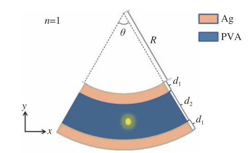
Fig. 1 Schematic diagram of the MDM structure model composed of silver and PVA, in which: the orange area represents the silver film with a thickness of d1;the blue area represents the dielectric PVA with a thickness of d2, the inner radius of the upper silver film is R, and the central angle corresponding to the structure is θ图1 银和PVA组成的MDM结构模型示意图,其中橙色区域代表银膜,其厚度为d1;蓝色区域代表电介质PVA,其厚度为d2,上层银膜内半径为R,结构所对应圆心角为θ
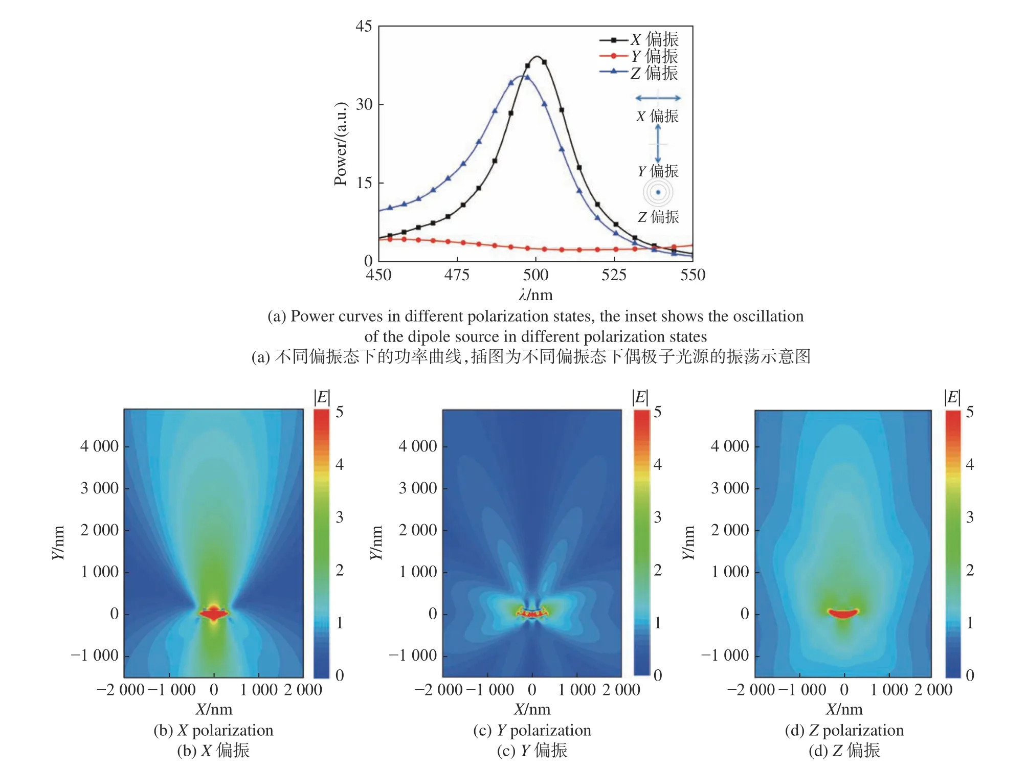
Fig. 2 (a) Power curves of quantum dots in different polarization states; (b−d) electric field profiles of quantum dots in different polarization states at 515 nm wavelength图2 (a)不同偏振态下量子点的功率曲线;(b−d)不同偏振态的量子点在波长515 nm处的电场分布图

Fig. 3 Power curves and Purcell factors of quantum dots for the MDM structures with different center angles图3 在MDM不同圆心角下量子点的功率曲线及珀塞尔因子
It can be seen from the electric field profiles that the far-field electric field can be enhanced by the polarization of the dipole light source in thexandzdirections. Therefore, it can be concluded that when the radiation direction of quantum dots is perpendicular to the MDM structure, the MDM structure will be coupled with fluorescence emission to enhance the directional emission of the quantum dots, and a more obvious fluorescence enhancement effect will be yielded in thex-polarization state.Therefore, in the following research, we will select the quantum dots in thex-polarization state for research and analysis.
3.2 Effects of the MDM structure with different central angles on fluorescence emission
Based on the above study, we know that the MDM structure will produce different fluorescence enhancement effects when coupled with the quantum dots in different polarization states. Next,we study the effect of different arc lengths corresponding to the changing central angle on fluorescence emission. Here, we compared and analyzed the MDM structures with the central angleθranging from 0° to 180°. Seven values were selected with 30° as the step size, and other parameters remained unchanged. The power curves and radiation attenuation rate curves were obtained through numerical simulation, as shown in Figure 3 (Color online). As can be seen from Figure 3(a), compared with the fluorescence emission of quantum dots in the bare light source (corresponding to the central angle of 0°) and in the flexible PVA substrate, the MDM structure demonstrates good far-field fluorescence enhancement effect at different central angles.This finding indicates that the non-planar flexible structure has stable performance in enhancing the fluorescence emission. In addition, when the central angle corresponding to the structure is 60°, the farfield fluorescence peak is the maximum so that the optimal luminescence enhancement effect can be achieved. As can be seen from Figure 3(b), the radiation attenuation rate (Purcell factor) of the MDM structure coupled with fluorescent QDs has a significant peak in the wavelength range of 450−550 nm,indicating that the fluorescence emitted by the dipole light source resonates in the FP cavity of the MDM structure and achieves about 5.3 times of fluorescence enhancement.

3.3 Effects of the MDM structures with different radius on fluorescence emission
Then we analyzed the effect of radius on fluorescence enhancement, which is another factor affecting the arc length. The central angle corresponding to the structure wasθ=60°. The MDM structures with the minimum internal radiusRranging from 350 nm to 750 nm were compared and analyzed. Five values were selected with the step size of 100 nm, and other parameters remained unchanged. The obtained power curves and radiation attenuation rate curves are shown in Fig. 4 (Color online). As can be seen from the power curves in Figure 4(a), compared with the quantum dot emission in the flexible PVA substrate, all the MDM structures have an emission peak in the waveband of 450−550 nm. Compared with the planar structure with an infinite radius, the flexible MDM structure will enhance the far-field fluorescence intensity.When the internal radius of the structure is 450 nm,the power peak value reach the maximum. With the increase of the internal radius, the fluorescence emission peak will be slightly red-shifted, because the structure with a smaller size can be easily coupled with short-wavelength fluorescence emission to achieve fluorescence enhancement. This also indicates that the different bending radians of the MDM structures used in flexible light-emitting devices will slightly affect the wavelength of fluorescence enhancement. This result provides theoretical guidance for the research and development of flexible light-emitting devices based on MDM structures. As can be seen from the radiation attenuation rate curves in Figure 4(b), when the MDM structure is coupled with fluorescent quantum dots, the radiation attenuation rate has an obvious peak; when the structure radius is 450 nm, the radiation attenuation rate reach its maximum.

Fig. 4 Power curves and Purcell factors of quantum dots for the MDM structures with different radii图4 MDM半径不同时,量子点的功率曲线及珀塞尔因子
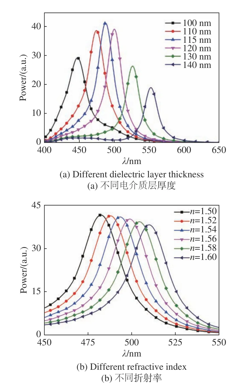
Fig. 5 Luminous power curves of quantum dots for the MDM structures with different dielectric layer thicknesses and refractive indexes图5 MDM电介质层厚度及折射率不同时量子点发光功率曲线
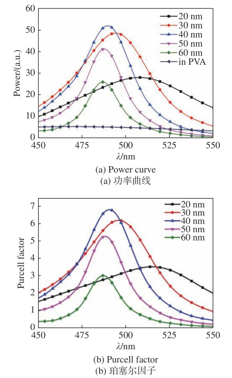
Fig. 6 Luminous power curves and Purcell factors of quantum dots for the MDM structures with different upper and lower silver film thicknesses图6 MDM不同上下层银膜厚度时量子点发光功率曲线和珀塞尔因子
3.4 Effects of the MDM structures with different dielectric thicknesses and refractive indexes on fluorescence emission
Through the above study, it can be concluded that when the internal radius of the structure is 450 nm, FP cavity mode can be best coupled with quantum dot fluorescence to increase the fluorescence enhancement factor of quantum dots. To explore the specific influence of intermediate dielectric thickness and refractive index variation on the tunability of fluorescence emission wavelength,we first compared and analyzed the MDM structures with intermediate dielectric thicknessd2varying from 100 nm to 140 nm. Six values were selected with 10 nm as the step size. The central angle corresponding to the structure wasθ=60°, and the internal radius of the structure was 450 nm. Other parameters remained the same. As shown in Figure 5(a) (Color online), the fluorescence emission peak of the structure will be red-shifted with the increase of intermediate dielectric layer thickness. The far-field fluorescence emission peak reach its maximum when the dielectric layer thickness is 115 nm.
By using this characteristic, the MDM structures with different dielectric thicknesses can be coupled with different fluorescence emission wavelengths of quantum dots to achieve the flexible tunability of directional emission enhancement of the fluorescence in different target colors. Secondly,we studied the fluorescence emission power when the MDM structures with different dielectric refractive indexes were coupled with quantum dots. The obtained results are shown in Figure 5(b) (Color online). It can be seen that, the change of refractive index of intermediate dielectric layer in the MDM structure has little influence on fluorescence enhancement effect. With the increase of refractive index of the intermediate layer, the fluorescence peak is continuously red-shifted and reduced slightly.
3.5 Effects of the MDM structures with different silver-film thicknesses on fluorescence emission
Through the study of the influence of the above multiple structural parameters on fluorescence emission, it can be concluded that the central angle and internal radius of the structure have a certain influence on the value of fluorescence emission peak,whose position, however, mainly depends on the refractive index and thickness of intermediate dielectric layer of the structure. Next, we studied the effects of different upper and lower silver film thicknesses on fluorescence emission. We compared and analyzed the MDM structures with silver film thicknessd1changing from 20 nm to 60 nm. Five values were selected with the step size of 10 nm, the central angle corresponding to the structure wasθ=60°,the minimum internal radius of the structure was 450 nm, and the thickness of intermediate dielectric layer was 115 nm. Other parameters remained unchanged. The results are shown in Figure 6(Color online). When the thickness of upper and lower silver films is 40 nm and the wavelength is 490 nm, the far-field fluorescence peak reach the maximum.
3.6 Effects of metal and metal-dielectric structures on fluorescence emission
In order to receive highly directional outgoing light from quantum dots, we designed an MDM arc structure with an internal radiusR=450 nm, a central angle 60°, an upper/lower silver film thicknessd1=40 nm and a dielectric layer thicknessd2=115 nm. In order to study the directional fluorescence emission effect of this structure, we comparatively studied the far-field fluorescence-induced electric field distribution of M, MD and MDM are structures at the central wavelength of 490 nm, and obtained the results as shown in Figure 7(a)−7(c)(Color online). It can be found that compared with M and MD nanostructures, the flexible MDM structure can achieve stronger far-field fluorescence enhancement and highly directional emission. The farfield power curves and Purcell enhancement curves of flexible M, MD and MDM structures are shown in Fig. 7(d)−7(e) (Color online). It can be found that compared with flexible M and MD structures, the far-field power of flexible MDM structure is significantly enhanced. As can be seen from Figure 7e,the radiation attenuation rate of MDM structure at 490 nm wavelength increases by a factor of about 7,indicating that the use of this structure can enhance the fluorescence quantum efficiency by a factor of about 7. Compared with M and MD structures, the MDM structure can effectively enhance and directionally modulate the fluorescence emission due to the excellent characteristics of its FP cavity.

Fig. 7 The electric field distribution diagrams, power curves and Purcell factors for quantum dots in metal-dielectric-metal structure, metal-dielectric structure and metal structure at 490 nm wavelength图7 490 nm波长下,金属-电介质-金属结构、金属-电介质结构、金属结构中量子点发光的电场分布图、功率曲线和珀塞尔因子
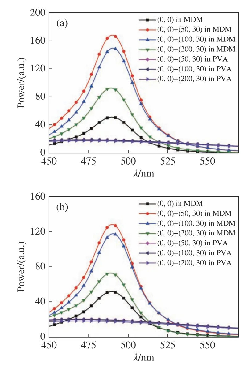
Fig. 8 Far-field fluorescence power curves of (a) two coherent dipole sources and (b) two incoherent dipole sources located at different positions in the MDM structure and flexible PVA substrate图8 位于MDM结构和柔性PVA基底中不同位置的(a)两相干光源和(b)两非相干光源的远场荧光功率曲线
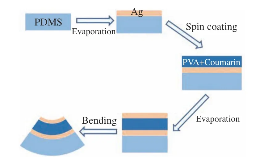
Fig. 9 Preparation process flow chart of MDM structure图9 MDM结构制备工艺流程图
3.7 Effects of adjacent dipole light sources on fluorescence emission
Due to the relatively large structural size of the actual flexible light-emitting devices and the large number of light sources, we considered the influence of two adjacent dipoles on fluorescence emission. By analyzing the influence of the relative position between the two dipole sources in the flexible MDM structure and the flexible PVA substrate on far-field fluorescence emission, their far-field fluorescence power curves were obtained, as shown in Figure 8 (Color online). The power curves of two coherent and two incoherent dipole sources are given in Figure 8(a) and Figure 8(b) respectively. It can be seen that the emission of two dipole sources,either coherent or incoherent, is stronger than that of a single dipole source. With the decrease of the relative position between the two dipole sources, the value of fluorescence emission peak will increase gradually, but its position will remain unchanged.This is because when two adjacent dipole sources are close to each other, the emitted light from the sources will interact with each other in the near field to increase the emission intensity. Secondly, in a flexible PVA substrate, the far-field fluorescence emission of two dipole sources is not affected by their relative position. Compared with the doubledipole emission in a flexible PVA substrate, the double-dipole or single-dipole emission of flexible MDM structure can achieve far-field fluorescence enhancement. This finding is of certain guiding significance to applying the proposed MDM structure in flexible light-emitting devices.
4 Experiment and results analysis
In order to verify that the flexible MDM structure can enhance the luminescence of fluorescent substances, coumarin 6 is selected here as the fluorescent substance for experimental verification. The process for preparing the MDM structure is shown in Figure 9 (Color online). The glass slide was cleaned with alcohol in an ultrasonic cleaner for 15 min. After air-drying, a layer of polydimethylsiloxane (PDMS), which was a transparent flexible medium, was placed on the glass slide. A silver film with a thickness of 40 nm (99.999% purity)was prepared by depositing a silver layer on PDMS through LN-1084SC organometallic vapor deposition system and adjusting the deposition rate(~1.0 nm/min). Then, 100 μm coumarin 6(C20H18N2O2S, MW=350; the central wavelength is 515 nm after the dissolution in alcohol) was mixed with 3% aqueous PVA solution (MW=44.05). The required PVA dielectric layer thickness of 115 nm could be obtained by spin-coating the solution on silver layer at the set speed of 3 000 r/min[22]. Subsequently, a second silver layer (40 nm) was evaporated by vapor deposition on the PVA layer to obtain the MDM structure, as shown in Figure 10.
The sample was placed on the optical microscope platform. The bent MDM structure was observed with an optical microscope. Its bright field image and dark field image under 375 nm laser irradiation are shown in Figure 11 (Color online). It can be seen that the bent MDM has a certain radian, and that the fluorescent material at the focal point emits blue and green light under 375 nm laser irradiation,as observed from the designed MDM structure. The existence of irregular texture on the surface of MDM structure indicates that the evaporation process has a certain influence on the final morphology of MDM structure. Subsequently, a continuous laser with a wavelength of 488 nm was used to irradiate the sample, and the PL of the sample was collected by spectrometer. The collection process of structural PL is shown in Fig. 12.
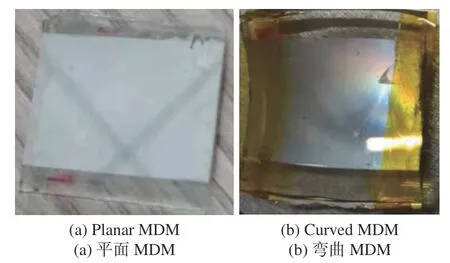
Fig. 10 MDM structures. (a) planar; (b) curved (top view)图10 MDM结构。(a)平面;(b)弯曲(俯视图)
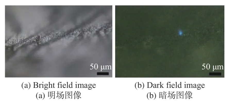
Fig. 11 (a) Bright field image of MDM structure under optical microscope; (b) dark field luminescence image under 375nm laser irradiation图11 光学显微镜下MDM结构的(a)明场图像;(b)375nm激光照射下的暗场发光图像

Fig. 12 PL collection process图12 PL收集过程
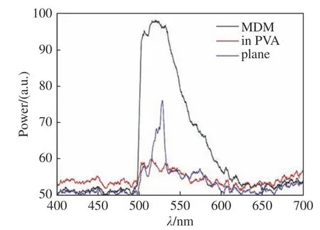
Fig. 13 PL curve obtained from the experiment图13 实验所得PL曲线
The PL of coumarin in PVA on PDMS substrate and that of the obtained planar MDM structure and the bent MDM structure were detected. The collected PL curves are shown in Figure 13 (Color online). It can be seen that compared with the quantum dot emission in PVA and planar MDM structure, the flexible curved MDM structure can further enhance the fluorescence emission of quantum dots, which is consistent with theoretical analysis results. In addition, this structure has a relatively wide fluorescence emission spectrum.However, in the experimental process, the mixingratio error of PVA solution will affect the thickness of dielectric layer after spin-coating, and then affect the position of fluorescence emission peak. In addition, the thickness, homogeneity and bending angle of the evaporated Ag film have certain influence on fluorescence enhancement factor.
5 Conclusion
In this paper, a flexible curved MDM structure is proposed. The simulation and experimental results show that this structure can achieve the directional emission enhancement of far-field fluorescence. By using the FDTD method, we systematically studied the effects of different radius central angles, dielectric thicknesses, dielectric refractive indexes and silver film thicknesses on fluorescence enhancement as well as the effects of adjacent dipole sources on fluorescence emission. The results show that the local undulations and arcs of the MDM structure can promote fluorescence enhancement in that they can not only highly modulate the directionality of the outgoing light of quantum dots,but also improve the radiation attenuation rate of quantum dots. In addition, different structure radius and central angles can enhance the far-field fluorescence emission of flexible curved MDM structure and achieve good directionality. The tunability of target wavelength can be achieved by changing the refractive index and thickness of the dielectric layer.Compared with metal structure and metal-dielectric structure, the curved MDM structure has the most significant fluorescence enhancement effect. When the quantum dots are located in the middle of the MDM structure, the high directionality of far-field fluorescence emission can be achieved, and the farfield power enhancement factor can reach about 7.This study verifies the applicability of flexible MDM structure in flexible devices, demonstrating that this structure can be used to enhance the luminescence intensity of flexible light-emitting devices and achieve high-sensitivity fluorescence sensing.
——中文对照版——
1 引 言
荧光发射具有高灵敏、光谱可调等众多优势,已经在光学成像、生物传感、LED显示等领域取得了飞速发展。特别是柔性LED由于具有可弯曲、结构成本低、轻薄便捷、性能优良等特点,使得其在折叠手机、曲屏电视、柔性电子书等显示器件、柔性光源和可穿戴设备等方面具有广泛的应用。例如:2011年,Wang等人提出了一种基于柔性基底的高效OLED,对于绿色荧光实现了高达60%的外量子效率[1]。2013年,Kim等人提出了一种可用于可穿戴显示器的OLED,在弯曲半径为5 mm的1 000次循环弯曲后依然具有一定的稳定性[2]。2020年,Shan等人提出了一种可穿戴和可调色的钙钛矿发光/检测双功能光纤,具有最窄的~19 nm的发光光谱,可以同时发射和接收信号[3]。
但传统荧光发射仍存在一些局限性,比如依赖于光子自发发射的荧光在所有方向上均是各向同性的,这也就意味着荧光性质基本上与观测方向无关,使得荧光发射的量子产率较低。而对于低量子产率的荧光团,进一步增强荧光发射可以显著改善相关光学系统的性能(例如,传感灵敏度,成像质量和发光亮度、稳定性等)[4-8]。因此为了提高实际应用中的荧光发射效率,满足现代荧光器件小型化的要求,以一种经济有效的方式控制发射方向,将原始的各向同性发射转化为定向发射是非常重要的。这一研究近年来也引起了相当大的关注,对于光学传感器、显示器和发光器件有很大的价值[9]。
之前的工作已经证明了荧光与金属纳米结构[10]、金属薄膜[4]、光子晶体[11-12]耦合可使得荧光定向发射增强。等离子体衬底由于强局域场增强和表面等离子体激元共振而增强荧光;光子晶体则由于光子带结构效应而增强荧光;通过在金属层上使用光栅、渔网结构或使用银和金的金属双层,可以实现荧光团与表面等离子体共振耦合的辐射增强。例如:2014年,Jiang等人[13]设计了顶部是1D周期Ag光栅的亚波长Ag-PMMA-Ag腔结构,利用结构中的耦合效应,并通过改变介电层厚度、光栅周期、沟槽宽度和深度等结构参数使得染料分子的荧光发射光谱的半峰全宽变得最窄、荧光强度最大。2018年,Ren等人[14]设计研究了金属-介质-金属(MDM)渔网超表面结构的荧光发射过程,利用纳米尺度的金属元素与阵列之间的耦合效应产生的磁等离子体激元模式来控制增强荧光的波长,实现颜色可控的波长可调谐性。但这些结构制作工艺都比较复杂。基于简单的制作工艺,得到高的荧光定向发射增强仍是一个值得继续研究的课题。
MDM结构通过改变荧光发射的量子产率和方向性,可以有效地改变荧光发射特性[15]。而对于特定的电介质层厚度,荧光与法布里-珀罗腔模式的耦合可以使荧光向垂直于MDM结构的方向发射[4,16]。2016年,Shiekh等人[17]提出了一种MDM平面结构,其使用表面等离子体耦合发射(SPCE)来增强单分子发光,提高了SPCE的峰值强度和功率。2015年,Sharmistha等人[18]设计了MDM平面结构,通过改变金属层和介质厚度来控制荧光波长、角度依赖性和发射极化。但这些结构都是平面结构,不适合用于柔性显示或发光器件。
本文基于平面MDM结构可以使荧光向垂直于其表面发射的特性,在柔性结构的基础上,提出了一种MDM柔性结构,该结构中的法布里-珀罗腔模式与荧光相互作用也可以产生垂直于结构表面的光束发射,有望用于增强柔性发光器件中的定向发射。本工作首先研究了不同结构参数对量子点荧光发射的影响,得到可实现良好耦合的结构参数。然后,在此结构参数下,将其与金属-电介质结构、单层金属薄膜结构进行了对比。计算结果表明,MDM结构的局部起伏和弧度对荧光增强起促进作用,不但可以实现量子效率的增强,同时还可以得到高度定向的荧光出射。最后,通过实验验证了结构在柔性荧光增强方面的适用性。
2 模型和方法
为了验证MDM柔性结构在柔性发光器件中的适用性。本文提出了金属-电介质-金属(MDM)柔性结构,其三维模型主视图如图1(彩图见期刊电子版)所示。结构的最小内半径定义为R,上下层银膜厚度均为d1,中间层电介质厚度为d2,结构所对应的圆心角大小为θ,银的复折射率参数来自于Palik手册[19],聚乙烯醇(PVA)材料设为固定折射率1.52。设定该结构中电介质层的几何中心为原点O,通过原点O沿着水平方向为x轴、竖直方向为y轴。整个结构置于空气背景(n=1)中。利用时域有限差分方法(FDTD)对该MDM结构进行仿真计算,分析计算了结构和偶极子光源(可代表荧光分子或量子点)耦合时的荧光增强。偶极子光源位于原点O处,仿真区域为[x,y]=[−2.1∶2.1,−1.6∶5.0] μm,x和y方向的边界条件都是完美匹配层(PML)。影响荧光物质量子效率的重要因素之一是辐射衰减率,而辐射衰减率与荧光分子的量子效率呈正相关关系,辐射衰减率越大,荧光分子的量子产率也就越高。为了分析MDM结构对荧光发射的影响,引入珀塞尔因子F来定量表示荧光分子的辐射衰减率,其数学定义式如公式(1)所示[20-21]:

式中 Γrad表示柔性MDM结构存在时的辐射衰减率,Prad表示柔性MDM结构存在情况下辐射到远场的功率,相应地,和分别表示柔性MDM结构不存在时的辐射衰减率和辐射到远场的功率。
3 结果和讨论
3.1 MDM结构对不同振荡方向量子点发射的增强
在均匀介质中,量子点的发光是各向同性的。而在理论分析时通常选取几个典型的偏振态进行研究。本文中首先研究了量子点处于x,y,z3种不同偏振态对MDM结构中量子点荧光发射增强的影响。MDM结构最小内半径R=450 nm,Ag膜厚度d1=50 nm,电介质PVA层厚度为120 nm,结构所对应的圆心角θ=60°。通过仿真计算得到了MDM结构与不同偏振态的量子点耦合时的荧光增强曲线。从图2(a)所示的功率曲线可以发现:y偏振态下的量子点的远场荧光发射功率较小且其曲线无明显变化,表明该结构对y偏振态下的量子点荧光发射影响不大。同时,相比于量子点在y方向上的振荡,在x和z方向振荡时,可以实现较高的荧光增强,并且在x和z方向振荡时可以观察到一个明显的荧光发射峰。且当量子点处在x偏振态时,荧光发射峰值最大。因为在x和z方向振荡时,荧光辐射分布垂直于MDM结构,荧光与结构的相互作用增强,荧光通过和结构模式的耦合使得远场荧光功率增强。为了更直观地分析结构与不同偏振态下量子点的相互作用物理机制,得到了515 nm波长处x-y平面在3种偏振态下的电场分布图,结果如图2(b)~2(d)所示。从其电场图可以看出,偶极子光源在x和z方向偏振下,可使远场电场得到增强。因此可以得到:当量子点的辐射方向垂直于MDM结构时,MDM结构与荧光发射耦合,使得量子点的定向发射得到增强,并且在x偏振态下得到了更为明显的荧光增强效果。因此,在接下来的研究中,选择x偏振的量子点进行分析。
3.2 不同圆心角的MDM结构对荧光发射的影响
通过上面的研究得知,MDM结构与不同偏振态量子点耦合时会产生不同的荧光增强效果。接下来将研究圆心角变化所对应的不同弧长结构对荧光发射的影响。这里比较分析了圆心角θ从0°到180°变化的MDM结构,以30°为步长选取了7个值,其他参数保持不变。通过数值模拟计算得到了如图3所示的功率曲线和辐射衰减速率变化曲线。从图3(a)可以看出,相比于裸光源(对应圆心角为0°)和PVA柔性基底中的量子点荧光发射,MDM结构在不同的圆心角下都有很好的远场荧光增强效果。这一发现表明该非平面柔性结构具有稳定的荧光发射增强效果。此外,当结构所对应的圆心角大小为60°时,远场荧光峰值最大,可以达到最优的发光增强效果。从图3(b)中可以看到,MDM结构和荧光量子点耦合时的辐射衰减率(即珀塞尔因子)在450~550 nm波长范围内有一个明显的峰值,这表明在MDM结构的FP腔模式下偶极子光源发射的荧光产生共振,并且实现了约为5.3倍的荧光增强。
3.3 不同半径的MDM结构对荧光发射的影响
接着分析了影响弧长的另一因素—半径,对荧光增强的影响,结构所对应的圆心角θ=60°。比较分析了结构最小内半径大小R从350 nm到750 nm变化时的MDM结构,以100 nm为步长选取了5个值,其他参数保持不变。所得功率曲线和辐射衰减速率如图4所示。由图4(a)的功率曲线可以发现:相对于PVA柔性基底中的量子点发射,该MDM结构在450~550 nm波段内均有一个发射峰,并且相对于半径无限大的平面结构,该柔性MDM结构会使得远场荧光强度增强。当结构内半径为450 nm时,功率峰值最大。随着结构内半径的增大,荧光发射峰位有略微红移,这是因为尺寸较小的结构容易与短波长荧光发射耦合使荧光增强。这也表明MDM结构在实际应用于柔性发光器件时,不同的弯曲程度会对荧光增强的波长略有影响,为基于MDM结构的柔性发光器件的研发提供了一定的理论指导。从图4(b)辐射衰减率变化曲线可以得到,MDM结构和荧光量子点耦合时,辐射衰减率对应出现一个明显的峰值且当结构半径为450 nm时辐射衰减率最大。
3.4 不同电介质厚度及折射率的MDM结构对荧光发射的影响
通过以上研究可以得到:当结构内半径为450 nm时,FP腔模式和量子点荧光耦合效果最好,使得量子点的荧光增强倍数得到提高。为了探究结构中间层电介质厚度及折射率变化对荧光发射波长可调的具体影响,首先,比较分析了结构中间层电介质厚度d2变化的MDM结构,从100 nm到140 nm以10 nm为步长选取了6个值,结构所对应圆心角θ=60°,内半径为450 nm,其它参数保持不变。从图5(a)所示结果可以得到:随着中间电介质层厚度的增加,该结构荧光发射峰红移,且当电介质层厚度为115 nm时,远场荧光发射峰值最大。根据这一特性,可以利用不同中间层电介质厚度的MDM结构与量子点的不同荧光发射波长耦合,达到不同目标颜色荧光定向发射增强的灵活可调谐性。其次,研究了不同电介质折射率的MDM结构和量子点耦合时的荧光发射功率,结果如图5(b)所示,MDM结构中间电介质层折射率发生变化对荧光增强效果影响不大。随着结构中间层介质折射率的增加,荧光峰值不断红移且略有减小。
3.5 不同银膜厚度的MDM结构对荧光发射的影响
通过以上多个结构参数对荧光发射影响的研究得到:结构所对应圆心角大小、内半径这些因素对结构的发射峰值有一定的影响,而荧光发射峰位主要取决于结构中间层电介质折射率及厚度。接下来研究了不同上下层银膜厚度的MDM结构对荧光发射的影响。比较分析了结构上下层银膜厚度大小d1从20 nm到60 nm变化的MDM结构,以10 nm为步长选取了5个值,结构所对应圆心角θ=60°,结构最小内半径为450 nm,中间电介质层厚度为115 nm,其他参数保持不变。所得结果如图6所示,当上下层银膜厚度为40 nm,波长490 nm处远场荧光峰值最大。
3.6 金属、金属-电介质结构对荧光发射的影响
为了实现量子点高定向的出射光,设计了内半径R=450 nm、圆心角为60°、上下层银膜厚度d1=40 nm、电介质层厚度d2=115 nm的MDM有弧度结构。为了研究该结构的荧光定向发射效果,对比研究了有弧度的M、MD、MDM结构中心波长490 nm下的远场荧光电场分布,所得结果如图7(a)~7(c)所示。可以发现相比于M和MD纳米结构,MDM柔性结构可以实现较强的远场荧光增强和高度定向发射。M、MD和MDM柔性结构的远场功率曲线和珀塞尔增强曲线如图7(d)~7(e)所示。可以发现相比M和MD柔性结构,MDM柔性结构远场功率明显增强。从图7(e)可以看出,MDM柔性结构在波长490 nm处的辐射衰减率约为7倍,即表明该结构使得荧光量子效率增强倍数达到7倍左右。相比于M和MD结构,MDM柔性结构由于其FP腔的优异特性,可以对荧光的出射进行有效增强和定向调制。
3.7 相邻偶极子光源对荧光发射的影响
由于实际的柔性发光器件结构尺寸相对较大,所包含发光源的数量较多,因此考虑两个相邻偶极子对荧光发射的影响。通过分析位于柔性MDM结构中和柔性PVA基底中的两个偶极子光源之间的相对位置对远场荧光发射的影响,得到了其远场荧光功率曲线,如图8所示。其中图8(a)和图8(b)分别为两相干偶极子光源和两非相干偶极子光源的功率曲线,从中可以看到,无论是两相干光源还是非相干光源,两个偶极子光源的发射均比单个偶极子光源的发射强,并且,随着两个偶极子光源相对位置的减小荧光发射峰值逐渐增大,但是荧光发射峰位保持不变。这是因为当两相邻偶极子源之间距离较近时,光源的发射光会在近场相互作用使得发射强度得到增强。其次,在PVA柔性基底中,两偶极子光源的远场荧光发射不受其相对位置的影响。相对PVA柔性基底中的双偶极子光源发射,柔性MDM结构在双偶极子光源发射和单偶极子光源发射的情况下均可实现远场荧光增强。这一发现使得本文提出的MDM结构对应用于柔性发光器件有一定的指导意义。
4 实验制备及结果分析
为了验证柔性MDM结构可使得荧光物质的发光增强,这里选取香豆素6作为荧光物质进行实验验证。制备MDM结构的工艺流程如图9所示,将玻璃载玻片用酒精在超声波清洗器中清洗15 min,风干后在玻璃载玻片上放置一层透明柔性介质聚二甲基硅氧烷(PDMS)。用LN-1084SC型有机金属气相沉积系统在PDMS上沉积银薄膜,通过调节沉积速率(~1.0 nm/min)制备了厚度为40 nm的银膜(纯度99.999%)。然后用100 μM香豆素6(C20H18N2O2S,MW=350,溶于酒精后的中心波长约为515 nm)与浓度约为3%的聚乙烯醇PVA(MW=44.05)水溶液混合,在金属银膜表面进行旋涂,设置转速为3 000 r/min可以获得所需的约115 nm厚时PVA电介质层[22]。随后在PVA层继续使用气相沉积蒸镀第二层金属银层(40 nm),制备得到的MDM结构如图10所示。
将样品置于光学显微镜平台。采用光学显微镜观察弯折后的MDM结构,其明场图像和375 nm激光照射下的暗场图像如图11(彩图见期刊电子版)所示。从其明场和暗场图像可以看出经弯曲后MDM具有一定弧度,并且在375 nm激光照射下聚焦点处荧光物质发蓝绿光,与设计的MDM结构相似。MDM结构表面存在不规则纹理, 说明蒸镀过程对MDM结构的最终形貌有一定影响。随后,使用波长为488 nm的连续激光器照射样品,并通过光谱仪采集样品的PL,结构PL收集过程如图12所示。
检测得到了PDMS基板上PVA中香豆素的PL和所得平面MDM结构及将MDM结构弯曲之后的PL。采集到的PL曲线如图13(彩图见期刊电子版)所示,从中可以看出,相对于PVA和平面MDM结构中的量子点发射,柔性有弧度MDM结构可使得量子点的荧光发射得到进一步增强,与理论分析结果一致,并且具有相对较宽的荧光发射谱。但在实验过程中,PVA溶液的配比误差会影响旋涂后电介质层的厚度,进而影响荧光发射峰位。此外,蒸镀Ag膜的厚度、均匀性以及弯折角度会对荧光增强倍数有一定的影响。
5 结 论
本文提出了一种由金属-电介质-金属组成的MDM柔性有弧度结构,仿真模拟和实验结果表明,该结构可以实现远场荧光的定向发射增强,通过时域有限差分法系统地研究了该MDM结构的不同半径、圆心角、电介质层厚度和电介质层折射率及银膜厚度对荧光增强的影响,并研究了相邻偶极子光源对荧光发射的影响。计算结果表明MDM结构局部起伏和弧度对荧光增强起促进作用。不但可以对量子点出射光的定向性进行高度调制,同时可以提高量子点的辐射衰减率。不同结构半径和圆心角对MDM柔性有弧度结构的远场荧光发射都有一定的增强效果并且可以达到好的定向性,而且通过改变电介质的折射率和厚度可以实现目标波长的可调谐性。相比于单层金属结构和金属-电介质组成的复合结构,该MDM有弧度结构的荧光增强效果最为显著。当量子点位于MDM结构中间位置时,可以实现远场荧光发射的高度定向性,远场功率增强倍数达7倍左右。本文工作验证了MDM柔性结构在柔性器件中的适用性,可用于增强柔性发光器件发光强度,也可用于高灵敏度荧光传感。
猜你喜欢
杂志排行
中国光学的其它文章
- 《中国光学》约稿信
- 院士访谈
- 《发光学报》
——EI核心期刊(物理学类;无线电电子学、电信技术类) - Illustrating the Helmholtz-Kohlrausch effect of quantum dots enhanced LCD through a comparative study
- Fabrication of an ultra-narrow band-pass filter with 60 pm bandwidth in green light band
- Experimental investigation on propagation characteristics of vortex beams in underwater turbulence with different salinity
