Fabrication of an ultra-narrow band-pass filter with 60 pm bandwidth in green light band
2022-03-08WANGKaixuanCHENGangLIUDingquanMAChongZHANGQiuyu
WANG Kai-xuan,CHEN Gang,LIU Ding-quan ,MA Chong,ZHANG Qiu-yu,3
(1. Shanghai Institute of Technical Physics, Chinese Academy of Sciences, Shanghai 200083, China;2. School of Physical Science and Technology, ShanghaiTech University, Shanghai 200031, China;3. University of Chinese Academy of Sciences, Beijing 100049, China)
Abstract: Owing to the strong penetrating ability in the atmosphere, 532 nm-wavelength green laser has wide applications including free-space optical communications and laser three-dimensional mapping. A spectral filter, with a half-power bandwidth of less than 100 pm, is an important optical element to suppress the interference of background light. Therefore, an ultra-narrow band-pass filter based on optical interference film is designed and fabricated in this paper. The high and low refractive index film are made of tantalum pentoxide(Ta2O5) and silicon dioxide (SiO2), respectively. The designed optical thin films are deposited on a fused quartz substrate by double-ion-beam sputtering deposition method. The transmission spectra of the filters are measured by a tunable laser and a power meter. The half-power bandwidths of the filters are (60±2) pm, and the transmittance reaches 62.6%.
Key words: optical thin film; thin film filter; picometer bandwidth; green light band; space laser mapping
1 Introduction
The green laser with 532 nm wavelength has strong penetrating ability in the atmosphere, and the corresponding light source and photoelectric receiver have stable performance. The laser with this wavelength has a good application prospect in laser lidar, free-space optical communications, space laser remote sensing, 3D mapping imaging and other fields[1-4]. In order to reduce the interference of background light, especially the strong influence of solar radiation, a spectral filter with passband width below 100 pm (i.e. 0.1 nm) is needed to suppress the background light[5]. For such a filter, the main filtering techniques that can be adopted include: acoustoptic modulation, atomic filtering, Fabry-Perot (FP) etalon, thin film interference filtering, etc.[6-8].
For spaceborne optical instruments (especially those facing a deep space flight), reliability, high optical efficiency and light weight are the key factors to be considered, so the F-P etalon and thin film interference are the main technical options. E.Troupaki[5]et al. constructed a spectral filter by using the F-P etalon technique, and achieved 30 pm bandwidth spectral filtering on American ICESat-2 satellite for the elevation mapping of snow and ice,clouds and land. The instrument uses 6 laser beams for mapping. ICESat-2 is the only altitude-mapping satellite currently in use abroad. This kind of spectral filter has high requirements for temperature control. Moreover, it is difficult to arrange many spectral filters when quite a lot of laser beams are needed. In order to develop the space elevation mapping with more laser beams, we designed and fabricated a bandpass filter with a target bandwidth of 60 pm based on precision optical thin film.
2 Design and fabrication of film system
Several related subnano-level spectral filtering techniques are listed in Table 1, each of which has its own characteristics. In this paper, the spectral filtering technique based on thin film interference is adopted.

Tab. 1 Comparison of main filtering techniques for sub-nanometer spectrum in visible light band表1 可见光波段的主要亚纳米光谱滤波技术比较
2.1 Design of filtering film system
For the band-pass filter with very narrow halfpower bandwidth, the F-P structure with a single resonator is adopted to form a filter with all-medium film layer considering the actual deposition error of each layer of film. Its waveform is comparable to that of a filter based on F-P etalon, and its spectrum rectangularity can be improved by increasing the interference order of spacer layer. Ta2O5is selected as the high-index film layer and is applicable to ultra-narrow band-pass filters, such as the Dense Wavelength Division Multiplexing (DWDM)filter used in 4G and 5G optical communications,due to its excellent physical and chemical stability and transparency in near-ultraviolet, visible and short-wave infrared bands[9-11]. SiO2is selected as the low-index film layer, which has good transparency, high physical and chemical stability and good thermal matching with the substrate made of fused quartz due to the sharing of the same material.Fused quartz (JGS-1, 4 mm thick) is selected as the substrate of the ultra-narrow band-pass filter due to its good thermal stability[12].
The filtering film system is designed as Sub./(1H 1L)101H 2L 1H (1L 1H)101L / Air, where H and L respectively represent the Ta2O5and SiO2film layers with an optical thickness of 1/4 central wavelength, which is the laser wavelength of 532 nm. The low-index film layer 2L is designed as a spacer, since it has smaller linear expansion coefficient and refractive-index temperature coefficient,so has more stable filter spectrum compared with 2H spacer. Of course, this film system is also more sensitive to the incident angle. This is a Fabry-Perot structure with a single resonator, consisting entirely of dielectric films.
The passband width can be approximated by Equation (1)[13-14]:

wherenHandnLare respectively the refractive indices of the high and low index film layers,ngis the refractive index of the substrate (ng=1.445),xis the number of the high-index film layers in the reflective film stack (x=11),λ0is the central wavelength(λ0=532 nm), andmis the interference order of the filter (m= 1). At 532 nm wavelength,nHandnLare assumed to be 2.108 and 1.442[14]respectively for calculation, and the design value of half-power bandwidth is determined as 0.053 nm (53 pm). The bandwidth values calculated by Equation (1) are a series of separated values, among which 53 pm is the calculated value close to the target. Due to the influence of various technological factors in the actual film growth process and the existence of filmthickness monitoring error, the spectral passband will be widened to a certain extent.
Through “Film Wizard” film design software,the transmission spectrum curve of bandpass filter was obtained from the designed film system, as shown in Figure 1 (Color online). No antireflective film layer was designed on the other side of the substrate. When the light absorption of the film layer was not considered, the peak transmittanceTPreached 93% and the value of half-power bandwidth was 57 pm, it is little different from the result of Equation (1). When the light absorption of the film layer was considered and the extinction coefficients of the high and low index film layers (kH=1.5×10⁻⁵,kL=1.0×10⁻⁵) were introduced[15], the peak transmittanceTPdropped to 74% and the value of half-power bandwidth increased to 65 pm. In the band with wavelengths less than 531.5 nm and larger than 532.5 nm, another filter with a wider passband would be used for spectral interception.
2.2 Film fabrication
For ultra-narrow band-pass filters, their optical films are mainly prepared with two techniques: (1)Ion Beam Assisted Deposition (IBAD); (2) Dual Ion Beam Sputtering (DIBS). Comparatively speaking,the film prepared by DIBS technique is denser, and the film and its components are more reliable and stable[16-19]. In this paper, the DIBS technique is used to prepare thin films. The layout and working diagram of the vacuum chamber of the coating equipment are shown in reference[15]. The sputtering ion source RF16 is the main ion source, generating the converging high-energy (Ar+) ion beams to sputter the targets (Ta and SiO2targets). The (O2+and Ar+)mixed ion beams generated by RF12 are used to bombard the film in growth to achieve full oxidation and dense growth of the film. The purity of the targets is ≥99.99%. When the film was coated,the workpiece plate rotated at a high speed up to 800 r/min.
In the process of film deposition and growth,the Optical Monitoring System (OMS) emitted 532 nm light, which passed directly through a monitoring glass and was received by a detector. Then,an electrical signal was output from the detector to observe the change of light intensity. By substituting the filtering film system designed in Section 2.1 into the programming software “Film Maker”, the intensity change and trend of the transmitted light signal can be calculated and displayed, as shown in Figure 2. As can be seen from Figure 2, the optical monitoring signal passing from the 14thlayer to the 31stlayer tends to be flat with a small variation,which will bring a large monitoring error. This requires improving the monitoring method by introducing a new monitoring glass when starting the film coating in an insensitive layer. The “OptiLayer”film software is used to analyze the sensitivity of each film layer. The sensitivity represents the degree of the influence of film layer error on filter spectrum. The lower the sensitivity, the less the influence of the error. The sensitivity of each film layer is given in Fig. 3. It can be seen that the sensitivity increases rapidly from the 13th layer. Therefore,it is necessary to increase the variation amplitude of optical monitoring signal in the film layers 14−31 in order to improve the monitoring accuracy of the film layers. Therefore, after the deposition of the 12thlayer, a new monitoring glass should be used to monitor the deposition and growth of the next 32(13thto 44th) layers, thereby effectively improving the monitoring accuracy of the sensitive film layers.The Fig. 4 shows the change of optical monitoring signal with the increase of film layers after introducing two monitoring samples. It can be seen that the amplitude of variation is significantly increased.

Fig. 1 Transmittance spectra of the designed ultra-narrow band-pass filter图1 设计的超窄带滤光片透射光谱
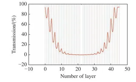
Fig. 2 Variation of the transmittance of optical signal as a function of the number of film layers图2 透射光控信号随膜层的变化
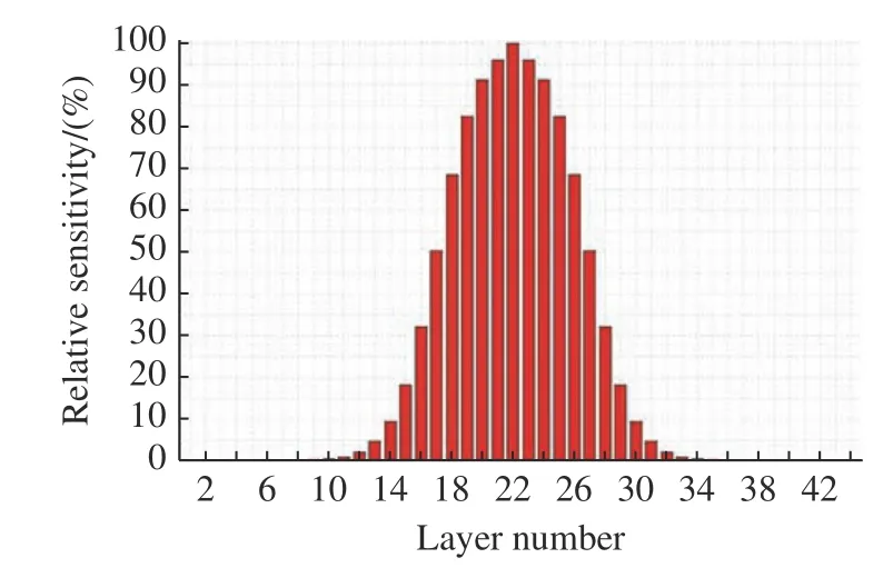
Fig. 3 Sensitivity of film layer error on filter spectrum in each layer图3 各个膜层误差对光谱影响的敏感度

Fig. 4 Change of optical monitoring signal by using two separated monitor glass plates图4 分成两片监控后光控信号的变化
As can be seen from Fig. 4(b), the monitoring signal in the 20thlayer on the monitoring glass 2 (the 32ndlayer as a whole) has hardly changed, so the time monitoring method is adopted for this layer.This is a layer of SiO2film. The average deposition time of the 3 layers of SiO2film in front of this layer is calculated by the control computer, as the deposition time of this layer. As can be seen from Fig. 3, the sensitivity of this layer is relatively low.The use of this method can achieve higher monitoring accuracy.
2.3 Spectral measurement
For an ultra-narrow band-pass filter with the bandwidth less than 1 nm, its transmission spectrum measurement requires more accurate instrument. The spectral resolution of the instrument should be better than 1/10 of the filter bandwidth. The spectral integral energy penetrating the filter is very small, so the instrument needs very high detection sensitivity and is required to effectively control electrical measurement noise and background light interference.
The spectral measurement setup is shown in Fig. 5. The light source is a supercontinuum laser source with a spectral range of 400−2000 nm, an output power of 8W, and a duty cycle of ≥99%.The light is led out of the optical fiber and is vertically incident on the surface of the filter after collimation. After being collected, the light penetrating the filter is led by the optical fiber into a spectral analyzer (Yokogawa AQ6373B). The wavelength range of 531.5−532.5 nm is selected, and the sampling interval is 0.003 nm. The measured transmittance spectrum curve of the filter samples is shown in Fig. 6. Some fluctuations can be seen on both sides of the passband. These fluctuations are measurement noises and the curve is not smoothed.

Fig. 5 Schematic diagram of the transmission spectrum measurement setup图5 透射光谱测量装置示意图

Fig. 6 Measured transmission spectrum of the ultranarrow band-pass filter图6 测量的超窄带通滤光片的透射光谱
3 Analysis and discussion
3.1 Analysis of measurement spectrum
The comparison between Fig. 6 and Fig. 1 shows that the actually measured spectral passband is broadened and the peak transmittance is somewhat reduced. The specific data comparison is listed in Table 2.

Tab. 2 Data of measured and designed transmission spectrum表2 测量和设计的透射光谱数据
The film formed after actual deposition has a certain light absorption. In the process of deposition and growth, the optical control of film layer thickness always has some errors. Based on these two reasons, the actually measured spectrum is inconsistent with the designed spectrum.
(1) Effect of film absorption. The film absorption reduces the transmittance of optical energy, so that the transmittance of the spectral curve will decrease as a whole. As can be seen from Fig. 1 for this kind of ultra-narrow band filter, the peak transmittance is much smaller than that without film absorption, and the transmittance decreases a little at the wavelength far away from the peak wavelength.Thus the bandwidth corresponding to the half-peak value increases, and theBvalue is different from theAvalue, as shown in Table 2.
(2) Effect of film thickness control error. The control error of film thickness mainly includes the random error and the error caused by replacing the monitoring glass. The random error is usually very small, especially in the high-precision control system. Replacing the monitoring glass will change the initial growth state of the film, and thus will bring a certain error[20]. Due to the adoption of first-order vertical-transmission single-wavelength extremum monitoring method, the later deposited film layers can compensate for the error in the earlier film layers so that the optical thickness error of the whole film system will not be amplified. In order to investigate the influence of random error on the spectrum,the “OptiLayer” film software was used for simulation. An appropriate random error needs to be selected before simulation. Since the measured values of the filter bandwidth and central wavelength are not very different from the design values, the random error introduced should make the simulation results as close as possible to the design results, and should not be too large or too small. After several attempts,a random error of optical thickness equivalent to 10% of the passband width (i.e., 6 pm) was introduced to all layers. The simulation results are given in Fig. 7(a). Since the monitoring glass was replaced at the beginning of the 13th-layer plating, the effect of the random error of that layer on the spectrum needed to be investigated separately. For filters, the variations in passband width and central wavelength within 10% of the bandwidth are acceptable. After repeated attempts, the random error of each film layer was canceled, and a random error within 0.5% (i.e. 0.32 nm) of the optical thickness of the film layer was separately introduced into the 13thlayer to obtain the simulation results shown in Fig. 7(b). By using the DIBS deposition technique,the film thickness accuracy can be controlled to 0.5%.
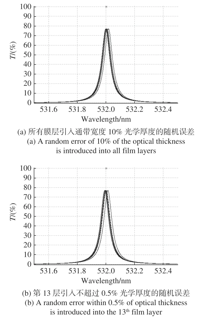
Fig. 7 Variation of spectral curves after randomly introducing the control errors图7 随机引入控制误差后的光谱曲线变化情况
As can be seen from Fig. 7, the introduction of these errors has little effect on the spectrum. The comparison with Fig. 6 indicates that the monitoring method used in this paper can control the random error within about 6 pm, thus forming a spectral passband with a width of 60 pm at 532 nm wavelength. The actual absorption of the film is larger than the set value, resulting in a further reduction of the peak transmittance. The bandwidth has no significant change, which is within the range of measurement error.

Fig. 8 Schematic diagram of the boundary between rough substrate surface and thin film图8 粗糙基片表面与薄膜分界示意图
3.2 Influence of substrate
The material and surface quality of the substrate have a certain influence on the spectral characteristics of this ultra-narrow band filter. The film deposition temperature is within the range of(100±5)℃, while the filter is usually used at normal temperature. Moreover, the environment may have temperature changes. Therefore, the linear expansion coefficientαof the film should be as close as possible to that of the substrate, and the refractiveindex temperature coefficients (dn/dT) of the film and substrate should be as small as possible. Alternative substrate materials are given in Table 3, including Crystal Quartz (CQ), several types of glass,and sapphire (Al2O3).
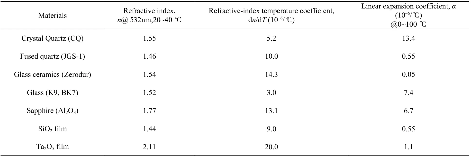
Tab. 3 Optical and thermal properties of substrates and thin films in this study[12, 21-22]表3 基片和薄膜的光学和热特性[12, 21-22]
The CQ and sapphire (Al2O3) given in Table 3 have birefringence (but the data in Table 3 is for ordinary light (O light)) and a large linear expansion coefficient, so they were not selected in this study.Glass ceramics was also not selected due to its high refractive-index temperature coefficient. Optical glass (K9, BK7, etc.) is usually doped with some substances containing heavy metals, and exhibits a transmittance decrease under space irradiation,which has been confirmed in our previous experimental studies. Part of the data is from Schott's website. In this study, the JGS-1 fused quartz from China was selected as the substrate material.
The surface quality of the substrate also affects the spectral performance of the filter. If the surface is not smooth enough, a thin transition layer with an uncertain refractive index will be formed at the interface between the film and the substrate, as shown in Fig. 8, whereds-fis the geometric thickness of the transition layer. The refractive indexns-fof the transition layer is determined by Equation (2),

whereρsis the volume proportion of the substrate material in the transition layer,nsandnfare the refractive index of the substrate and that of the first layer respectively. The optical thickness deviation caused by the transition layer can be given by Equation (3),

It can be seen that a rougher surface has a larger Δdvalue accordingly.
In this study, Δdshould not be larger than 6 pm(10% of the bandwidth). Assuming the volume proportionρsof 0.5 and the first layer of Ta2O5and considering the film layer sensitivity shown in Fig. 4, the roughness P-V of the substrate surface should be less than 2 nm, so the surface is an ultrasmooth surface.
3.3 Spectrum stability
The spectral measurement of the filter samples was made one month after the completion of cutting. The samples with qualified spectra were selected as products and applied in the laser mapping system. After one month of aging, the stress in the film has been released, the film system tends to be stable. The optical stability of the spacer layer 2L has the greatest influence on the spectrum, while the influence of other layers is relatively small. The spacer layer is made of the same material as the substrate. Under temperature control, small temperature changes will not generate new stresses. The change of the optical properties of the film with temperature will lead to spectral shift, which can be approximated by Equation (4)[12]:

whereλ0is the preset central wavelength, andλTis the central wavelength at the temperatureT;Pis the number of cycles in the reflector film layers,P=11;Qis the order of the spacer layer,Q=1;is the optical thickness of the high-index layerHat the temperatureT, andis the optical thickness of the low-index layer L at the temperatureT.
By substituting the film system parameters of the filter into Equation (4), the change of its transmission spectrum with temperature was determined.The spectral drift is about 54 pm at the temperature change of 10℃, about 16 pm at the temperature change of 3℃, and about 2 pm at the temperature change of 2℃. In the actual optical system where the filter is applied, the temperature control condition is set to ±2℃. The filter behaves stably during the actual laser mapping process in space.
4 Conclusion
By using Ta2O5and SiO2as high and low refractive index film materials respectively and fused quartz as the substrate, we prepared an ultra-narrow band filter with a half-power bandwidth of (60±2)pm, a central wavelength of 532.0 nm and a peak transmittance of 62.6% through DIBS deposition.When the insensitive film layers were deposited, the monitoring glass was switched, the accumulation amplification of errors were effectively controlled by using two monitoring glass plates one after another and first-order transmission extremum monitoring method. Finally, an ultra-narrow band filter with a measured half-power bandwidth of about 60 pm was obtained.
——中文对照版——
1 引 言
波长为532 nm的绿色激光在大气层中具有很好的穿透能力,相应的光源和光电接收器的性能稳定。该波长的激光在激光雷达、自由空间光通信、空间激光遥感和三维测绘成像等方面有着良好的应用前景[1-4]。为了减少背景光干扰,特别是太阳辐射的强烈影响,需要利用通带宽度在100 pm(即0.1 nm)以下的光谱滤波器来抑制背景光[5]。对于通带宽度小于0.1 nm的光谱滤波要求,可采用的主要技术方式有:声光调制技术、原子滤波技术、法布里-珀罗(F-P)标准具方式和薄膜干涉滤光技术等[6-8]。
对于空间光学仪器(特别是需要经历深空飞行的仪器),可靠性好、光学效率高和结构轻巧是需要重点考虑的因素,F-P标准具和薄膜干涉技术成为可选的主要技术方式。E. Troupaki[5]等用F-P标准具构建了光谱滤波组件,用于美国针对冰雪、云层和陆地进行高程测绘的ICESat-2卫星上,实现了30 pm带宽的光谱滤波,仪器用6束激光进行测绘。ICESat-2卫星是目前国外唯一正在使用中的高程测绘卫星。这种光谱滤波组件对温度控制要求较高,在需要较多激光波束时难以合理布局众多光谱滤波组件。为了发展更多激光波束的空间高程测绘,以精密光学薄膜为基础,设计制作了目标带宽为60 pm的带通滤光片。
2 膜系设计与制备
几种相关的亚纳米光谱滤波技术各有特点(见表1),本文采用薄膜干涉光谱滤波技术。
2.1 滤光膜系设计
对于半功率带宽非常窄的超窄带滤光片,考虑各层薄膜在实际沉积时存在的误差,采用单个谐振腔的F-P结构,形成全介质膜层的滤光片。其波形与采用F-P标准具得到的光谱波形相当,还可以用增加间隔层干涉级次的方法提升光谱的矩形程度。选用Ta2O5作为高折射率膜层,它在近紫外、可见光和短波红外波段具有非常好的物理化学稳定性和透明性[9-11],适合制作超窄带滤光片,如4G和5G光通信中使用的密集波分复用滤波器(DWDM)。本文选用SiO2作为低折射率膜层,SiO2具有良好的透明性和物理化学稳定性,与基片熔融石英材质相同,有良好的热匹配性。选用熔融石英作为滤光片基片,其热稳定性好,适合用作超窄带滤光片的基片[12],基片采用厚度为4 mm的JGS-1熔融石英。
滤光膜系设计为:Sub./ (1H 1L)101H 2L 1H(1L 1H)101L / Air。其中,H和L分别表示光学厚度为1/4中心波长的Ta2O5和SiO2膜层,中心波长就是532 nm激光波长。将低折射率膜层2L设计为间隔层,比起2H作为间隔层,它的线膨胀系数和折射率温度系数更小一些,滤光片的光谱也会更稳定一些。当然,这种膜系对入射光线的角度也会敏感一些。这是单个谐振腔的F-P结构,其完全由介质薄膜构成。
通带宽度计算,可以由公式(1)得到近似值[13-14],

其中,nH和nL分别为高低折射率膜层的折射率,ng为基片的折射率(取值1.445),x为反射膜堆内高折射率膜层数(取值11),λ0为中心波长(取值532 nm),m为滤光片的干涉级次(m= 1)。在波长532 nm处,nH和nL分别取为2.108和1.442[14]进行计算,得到半功率带宽的设计值为0.053 nm(即53 pm)。利用公式(1)计算得到的带宽值是一系列分离的数值,53 pm是接近目标的计算值。由于在实际薄膜生长的工艺过程中存在多种工艺因素的影响,还存在膜层的厚度监控误差,光谱通带会有一定程度的展宽。
将设计膜系代入Film Wizard光学薄膜设计软件,得到带通滤光片的透射光谱曲线,在图1(彩图见期刊电子版)中给出,在基片另一面没有设计减反射膜层。在不考虑膜层光吸收的情况下,峰值透过率Tp达到93%,半功率带宽的数值为57 pm,与式(1)差异不大;在考虑膜层光吸收的情况下,引入高低折射率膜层消光系数[15]:kH=1.5×10⁻⁵和kL= 1.0×10⁻⁵,峰值透过率Tp降低到74%,半功率带宽的数值增加到65 pm。在波长小于531.5 nm和大于532.5 nm的区域,将由另外的通带较宽的滤光片进行光谱拦截。
2.2 薄膜制备
对于超窄带滤光片,光学薄膜的制备技术主要有两种:(1)离子束辅助沉积技术(Ion Beam Assisted Deposition,IBAD);(2)双离子束溅射技术(Dual Ion Beam Sputtering,DIBS)。相对而言,DIBS技术制备的薄膜更加密实,薄膜和元件的可靠性和稳定性也更好[16-19]。本文采用DIBS技术制备薄膜,镀膜设备真空室内的布局和工作示意图见文献[15]。其中溅射离子源RF16为主离子源,它产生的高能会聚(Ar+)离子束用于溅射靶材料(Ta和SiO2靶);辅助轰击离子源RF12产生的(O2+和Ar+)混合离子束对生长中的膜层进行轰击,实现膜层的充分氧化和致密生长。靶材的纯度≥99.99%,镀膜时工件盘高速转动,转速达到800 r/min。
在薄膜沉积生长过程中,光学监控系统(OMS)发出532 nm波长的光直接穿过监控片,被探测器接收后输出电信号,用于观测光强度的变化。将前面2.1节中设计的滤光膜系代入编制软件Film Maker中,可以计算并显示出透射光信号的强弱变化和走势,如图2所示。从图2可以看出,从第14层到第31层光学监控的信号趋于平坦,变化幅度很小,这样会给监控带来较大误差。因此,需要改进监控方式,在一个不敏感层开始镀膜时切入一个新的监控片。用OptiLayer光学薄膜软件分析了各个膜层的敏感度,敏感度表示该膜层误差对滤光片光谱的影响程度,敏感度越低则误差的影响越小。图3中给出了各个膜层的敏感度,可以看出从第13层开始敏感度迅速增大。所以,必须提高第14到31层薄膜光控信号的变化幅度,才能提升膜层的监控精度。因此,在第12层薄膜沉积完成后,更换一个新的监控片来监控后面32层(第13到44层)薄膜的沉积生长,以有效提升敏感膜层的监控精度。图4给出了采用两个监控样品后,光学监控信号随膜层的变化情况,可见变化幅度明显提升。
从图4(b)可以看到,监控片2上的第20层(总第32层)的监控信号几乎没有变化,对该层采用时间监控方法。这是一层SiO2薄膜,由控制计算机计算出它前面3层SiO2薄膜沉积的平均时间,作为该层薄膜的沉积时间。从图3可以看到,该层薄膜的敏感度是比较低的。采用这样的方法总体可以得到更高的监控精度。
2.3 光谱测量
带宽小于1 nm的超窄带滤光片的透射光谱测量需要更加精确的光谱测量仪器。仪器的光谱分辨能力应该优于滤光片带宽的1/10;能够透过滤光片的光谱积分能量很小,仪器需要很高的探测灵敏度,同时能够有效控制测量电噪声和背景光干扰。
光谱测量装置如图5所示。光源选用超连续谱的激光光源,光谱范围为400~2000 nm,输出功率为8 W,占空比≥99%;光线由光纤导出,准直后垂直入射滤光片表面;透过滤光片的光线被收集后由光纤导入光谱分析仪器(日本横河公司生产的AQ6373B光谱分析仪),选定531.5~532.5 nm波长,采样间隔为0.003 nm。图6是测量得到的滤光片样品的透射率光谱曲线,在通带的两侧看到一些波动,这些波动是测量噪声,曲线没有经过平滑处理。
3 分析和讨论
3.1 测量光谱分析
对比图6和图1可以看出,实际测得的光谱通带有所展宽,峰值透过率也有所降低,具体数据对比见表2。
实际沉积制成的薄膜对光有一定的吸收;在沉积生长过程中,膜层的光学厚度控制也总是存在一些误差。基于这两方面原因,造成了实际测量光谱与设计光谱不一致。
(1)膜层吸收的影响。膜层的吸收会减少透过的光学能量,使得光谱曲线的透过率整体下降。从图1可以看出,对于这种超窄带滤光片,峰值透过率下降较多,离峰值波长较远处下降较少,这就使得半峰值对应的带宽增大,出现了表2中B值和A值的差别。
(2)膜厚控制误差的影响。膜层厚度的控制误差主要来自随机误差和更换监控片带来的误差,随机误差通常很小,特别在高精度控制系统中,更换监控片改变了薄膜的初始生长状态,会带来一定的误差[20]。由于采用了1级次的垂直透射式单波长极值监控方法,后续沉积的膜层对前面制成的膜层有误差补偿作用,可以使得整个膜系的光学厚度误差不被放大。
为了考察随机误差对光谱的影响,用OptiLayer光学薄膜软件进行模拟。在进行模拟之前需要选择合适的随机误差。由于滤光片的带宽和中心波长的实测值与设计值差距不大,因此引入的随机误差应使模拟结果尽量接近设计结果,不宜过大或过小。在进行多次尝试后,引入了光学厚度相当于通带宽度10%(即6 pm)的随机误差到所有膜层,并给出了模拟结果(图7(a))。由于在镀制第13层薄膜开始时更换了监控片,所以需要单独考察该层的随机误差对光谱的影响。对于滤光片而言,通带宽度和中心波长的变化在带宽的10%以内是可以接受的。同样进行多次尝试后,取消各个膜层的随机误差,再单独引入0.5%光学厚度(即0.32 nm)以内的随机误差到第13层薄膜中,并给出了模拟结果(图7(b))。对于用双离子束溅射薄膜沉积技术而言,膜厚精度控制到0.5%是可以实现的。
从图7可以看出,这些误差的引入对光谱的影响不大。对比图6可知,本文所用的监控方法可以把随机误差控制在约6 pm以内,因此能在532 nm波长处形成宽度为60 pm的光谱通带。薄膜的实际吸收能量比设定值要大一些,导致峰值透过率进一步降低,而带宽没有明显变化,变化量在测量误差范围内。
3.2 基片的影响
基片材质和表面质量对超窄带滤光片的光谱特性有一定的影响。薄膜沉积温度在(100±5)℃范围,滤光片通常在常温环境中使用,考虑到使用环境可能的温度变化,薄膜和基片的线膨胀系数应尽可能接近,薄膜和基片材料的折射率温度系数dn/dT应尽量小。可供选择的基片材料在表3中给出,这些材料是石英晶体(Crystal Quartz,shoux, CQ)、几种玻璃和蓝宝石(Al2O3)。
表3中,石英晶体(CQ)和蓝宝石(Al2O3)有双折射现象,表3中数据选用的是寻常光(O光)的数据,它们的线膨胀系数也较大,故在此研究中没有选用。微晶玻璃的折射率温度系数较高,也没有选用,光学玻璃(K9、BK7等)中通常掺杂了一些含有重金属的物质,空间辐照条件下其透过率会下降,本课题组以前的研究已经证实。部分数据来源于德国Schott公司网页。本研究选择中国牌号的JGS-1熔融石英作为基片材料。
基片的表面质量也会影响滤光片的光谱性能。不够光滑的表面,在薄膜与基片的界面处会形成一层折射率不确定的过渡薄层,如图8所示。其中ds-f是过渡层的几何厚度。这个过渡层的折射率ns-f由式(2)决定:

其中ρs是基片材料在过渡层的体积占比,ns和nf分别是基片的折射率和第1层薄膜的折射率。由过渡层引起的光学厚度偏差可以由式(3)给出:

可以看出,粗糙表面对应的Δd值也较大。在本研究工作中,Δd应该不大于6 pm(带宽的10%),按照ρs取0.5和第1层用Ta2O5薄膜来计算,结合图3考虑到膜层的敏感度,基片表面的粗糙度P-V值应该小于2 nm,属于超光滑表面。
3.3 光谱的稳定性
滤光片样品的光谱测量是在切割完成一个月后进行的,筛选出光谱合格的样品作为产品应用在激光测绘系统中。经过一个月的老化,薄膜中的应力已经释放,薄膜体系趋于稳定。对光谱影响最大的是间隔层2L的光学稳定性,其他膜层的影响相对小一些。间隔层与基片的材质相同,在温控条件下,小的温度变化不会产生新的应力。膜层光学特性随温度的变化会导致光谱的移动。光谱的移动量近似得[12]:

其中λ0是设定中心波长,λT是T温度下的中心波长;P是反射板膜层的周期数,这里取11;Q是间隔层的级次,这里取1;是T温度下高折射率膜层H层的光学厚度,是T温度下低折射率膜层L层的光学厚度。
将滤光片膜系参数带入公式(4),计算得到其透射光谱随温度变化的情况,即温度变化10 ℃时光谱漂移约54 pm,温度变化3 ℃时光谱漂移约为16 pm,温度变化2 ℃时光谱漂移约为2 pm。滤光片的实际应用光学系统,温控条件设置为±2℃,滤光片在空间实际激光测绘过程中表现稳定。
4 结 论
采用Ta2O5和SiO2分别作为高低折射率膜层材料,熔石英为基片,利用双离子束溅射沉积方法制备了半功率带宽为(60±2) pm超窄带滤光片,其中心波长为532.0 nm,峰值透过率达到62.6%。在不敏感膜层沉积时切换监控片,依次用2个监控片和1级次透射极值监控的方法,有效控制了误差的影响和积累放大,实测得到半功率带宽约为60 pm的超窄带滤光片。
猜你喜欢
杂志排行
中国光学的其它文章
- 《中国光学》约稿信
- 院士访谈
- Enhancing the fluorescence emission by flexible metal-dielectric-metal structures
- 《发光学报》
——EI核心期刊(物理学类;无线电电子学、电信技术类) - Illustrating the Helmholtz-Kohlrausch effect of quantum dots enhanced LCD through a comparative study
- Experimental investigation on propagation characteristics of vortex beams in underwater turbulence with different salinity
