Synthesis of hexagonal boron nitrides by chemical vapor deposition and their use as single photon emitters
2021-11-16HongweiLiuChaeYoungYouJingweiLiPatrickRyanGalliganJiawenYouZhenjingLiuYutingCaiZhengtangLuo
Hongwei Liu,Chae Young You,Jingwei Li,Patrick Ryan Galligan,Jiawen You,Zhenjing Liu,Yuting Cai,Zhengtang Luo
Department of Chemical and Biological Engineering,the Hong Kong University of Science and Technology,Clear Water Bay,Kowloon,999077,Hong Kong
Keywords:hBN CVD Controllable synthesis Single photon emission
ABSTRACT
1.Introduction
In the past couple decades,since the discovery of graphene as the first two-dimensional(2D)material[1],2D materials have attracted tremendous research attention due to their excellent electronic,chemical,and optical properties,stemmed from their2D layered structure[2,3].Typically,2D materials exhibit exceptional properties,distinctive to their bulk,such as bandgap transformation[4–8],extremely high carrier mobility[9,10],unusual thermal conductivity[11,12],conductivity transformation from superconductor to insulator[13]and topological electronic phases[14,15].Moreover,when different2D materials stack together as2D heterostructures,their properties can be further tuned according to stacking orders and twisting angles[16–20].Up to now,2D materials have demonstrated their strengths in various applications such as photodetectors[21–23],sensors[24,25],energy storage[26,27],catalysis[28–32],electrode materials[33,34],etc.
Among those prominent2D materials,hexagonal boron nitride(hBN)consists of sp2-bonded boron and nitrogen atoms in a hexagonal lattice[35].When the thickness is reduced to atomic level,hBN demonstrates a wide direct bandgap up to~5.9eV[36].Due to its atomic flatness and absence of dangling bonds,hBN can be used as a growth substrate for other2D materials,promoting the stabilization of2D materials-based devices[37–40].In this regard,monolayer and bilayer graphene electronic devices supported on hBN were fabricated,demonstrating mobilities increased by an order of magnitude higher than those on SiO2substrate[41].Recently,quantum emitters embedded in the point defects of hBN have been reported to be promising in application for single-photon emissions(SPEs),a key component for quantum communication and quantum technologies[42–44].The point defects can generate deep energy levels within the bandgap of hBN and thus serve as emission sites.SPEs in hBN make it possible to sufficiently integrate two-dimensional single-photon sources onto electronic chips and promote the development of quantum photonics.
The extraordinary properties of hBN have attracted the research community to achieve reliable and controllable synthesis methods for hBN.The preparation of hBN can be realized by two routes:top-down methods including mechanical or liquid exfoliation,and bottom-up strategies such as molecular beam epitaxy or chemical vapor deposition(CVD).Among these methods,CVD is the most promising due to its potential for mass production and flexible controllability during the growth process.It is therefore crucial to understand the CVD growth process and to adjust parameters such as growth temperature,pressure,precursor concentration,substrates,etc.,so that hBN with the desired layer number,grain size,morphology,and other expected properties can be selectively obtained.
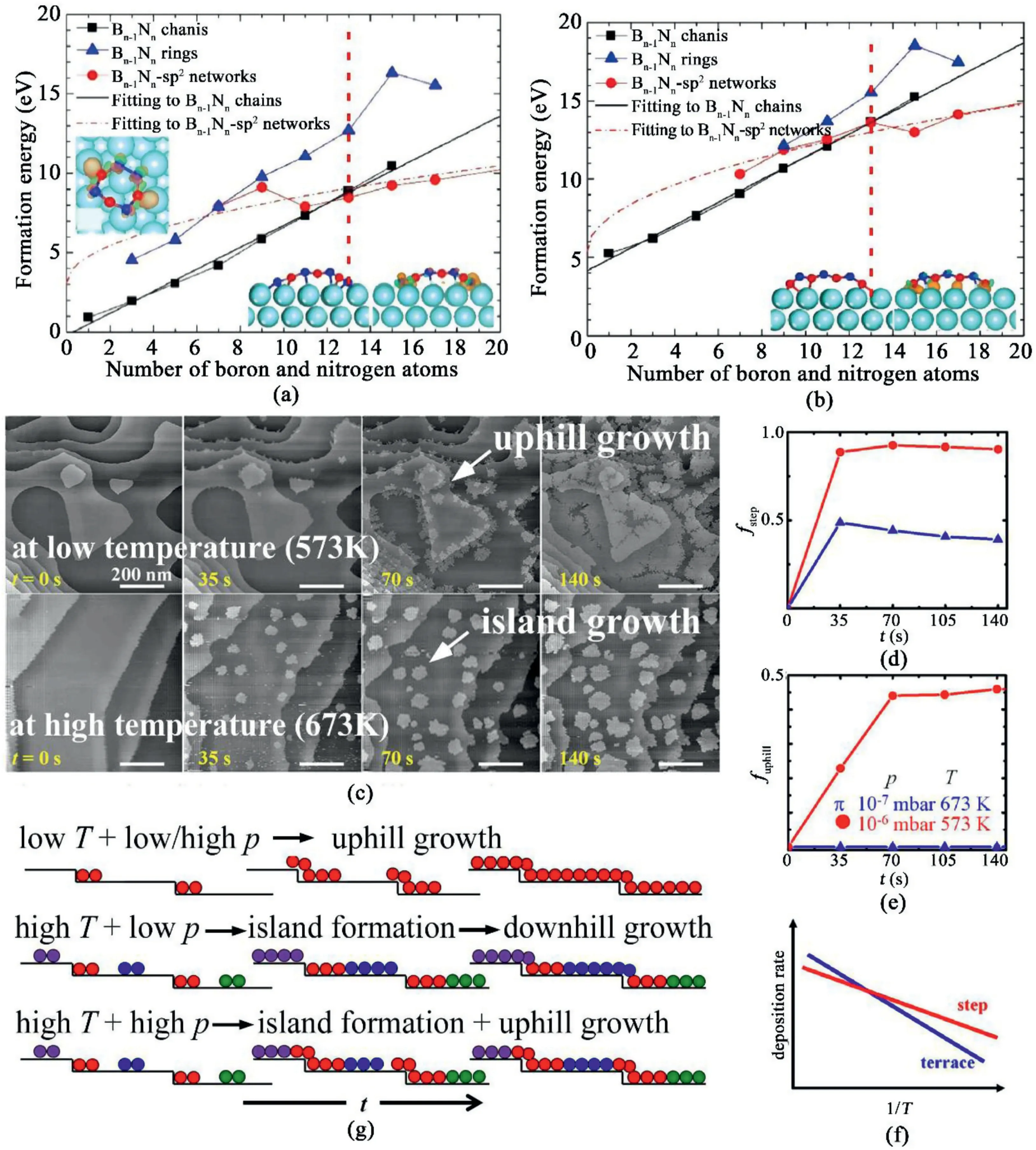
Fig.1.Growth mechanisms and kinetics of hBN grown by CVD.(a)and(b)Formation energies of Bn-1Nn and BnNn-1chains,rings,and sp2networks on Cu(111)surface versus the number of boron and nitrogen atoms in an hBN cluster[46].Reproduced from Ref.46with permission from The Royal Society of Chemistry.Copyright2019.(c)STM images revealing the growth kinetics of hBN grown on Pd(111)surface at low(top)and high(bottom)temperature.(d)Fractional coverage of hBN grains grown at the steps as a function of reaction time.(e)Fractional coverage of hBN grains grown at the descending step edges as a function of reaction time.(f)Hypothetical Arrehenius plot of deposition rate on the terraces and at the edges as a function of1/T.(g)Schematic hBN growth model under different growth conditions.Different colors refer to different rotational hBN domains[47].Reprinted with permission from Ref.47.Copyright2020American Chemical Society.
This review provides a thorough overview of recent progress on the controlled synthesis of hBN using chemical vapor deposition and its application as SPEs.We introduce mechanisms of hBN growth by describing the growth process at the initial stages,where the growth temperature and precursor pressure play important role to determine uphill or downhill growth.Newly developed strategies to control the domain size,growth orientation,morphology,layer number,and stacking order are subsequently discussed,including reducing of nucleation density to obtain large single crystal hBN grains,enhancing epitaxial growth to obtain oriented hBN grains,varying precursor diffusion kinetics to grow hBN grains with different morphologies and controlling growth parameters(e.g.,pressure,temperature,growth time and growth substrates)to obtain desired layer number and understand the related stacking order.Then,the origins of SPEs in hBN and several methods to selectively generate and tune the SPEs are addressed.Most of the works discussing about the origins of SPEs are conducted on the theoretical levels that different point defects(e.g.,boron vacancy,nitrogen vacancy and other complex defects)are potentially responsible for SPEs.Different strategies,such as plasma treatment,laser or electron beam irradiation,thermal annealing,engineered strain,etc.,are also discussed to generate and tune the SPEs in hBN.Several trials to utilize SPEs in hBN for practical applications are also introduced.Finally,this review gives an outlook on desirable hBN synthesis methods and further investigation of SPEs in hBN.Deeper research is in need to synthesize large scale hBN with stable and uniform emission sites for future industrial applications.
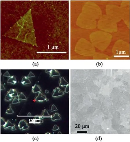
Fig.2.hBN synthesized on different substrates.(a)AFM image of hBN grown on Cu foil[49].Reprinted with permission from Ref.49.Copyright2012American Chemical Society.(b)AFM image of hBN grown on Pt foil[50].Reprinted with permission from Ref.50.Copyright2013American Chemical Society.(c)Dark field microscope image of triangular hBN on a Co(0001)substrate[51].Reprinted with permission from Ref.51.Copyright2013American Chemical Society.(d)SEM image showing hBN grown on Fe foil[52].Reprinted with permission from Ref.52.Copyright2016American Chemical Society.
2.Growth mechanisms and kinetics
Typically,the general growth mechanism for hBN includes the following three steps[45]:(i)decomposition of precursors(ammonia borane,borazine,etc.),where the precursors decompose into boron-and nitrogen-containing species under high temperature;(ii)deposition and nucleation,where the boron-and nitrogen-containing species deposit onto metal surface and combine into clusters;(iii)continuous growth,where these clusters grow into larger hBN islands and finally attach to form a continuous film.Such growth mechanisms of hBN on transition metals(e.g.,Cu,Ni)have been explored both experimentally and theoretically.
To understand the initial stages of hBN during CVD growth,the formation energy of hBN clusters with increasing amounts of atoms on Cu(111)substrate was calculated using density functional theory calculations(DFT)[46].It is found that for both Bn-1Nn(nitrogen-rich)and BnNn-1(boron-rich)clusters,the total atom amount of a cluster plays a critical role.When the cluster size is smaller than13atoms,hBN chains have the lowest formation energy and are more stable than hBN rings or sp2networks as shown in Fig.1a and b.On the other hand,when the cluster size is larger than13,a transformation from hBN chains to sp2networks will occur,resulting from the lowest formation energy of sp2networks.In addition to theoretical calculations,in situ investigation of the formation of hBN grown on Pd(111)surface by variable temperature scanning tunneling microscopy(STM)was also presented[47].It was found that the initial growth behaviors strongly depend on the growth temperatures and duration.Fig.1c shows the STM images of hBN growth at573K(top)and673K(bottom).At lower growth temperatures,the hBN crystals preferably nucleated at the Pd edges.As the temperature was elevated,the hBN crystals started to grow on the terraces to form hBN islands and then grew across the edges.The time-dependent changes of hBN grains coverage along the steps and on the terraces at low and high temperatures are shown in Fig.1d.It was observed that at low temperature(573K),the hBN grains nucleate at the edge,reaching89%coverage within35s,while at high temperature(673K),the coverage of hBN grains at edges would increase to less than50% then keep almost constant,indicating the simultaneous growth of hBN at the edges and on the terraces.Moreover,when the growth occurred along the step edges,the coverage of hBN at descending edges was always lower than that at the ascending edges(Fig.1e).The site-specific deposition rate Riwas suggested to follow the Arrhenius equation:Ri∝Niexp(-Ei/kBT)],where i represents different reaction sites(at the edges or on the terraces).The hypothetical plot is shown in Fig.1f and illustrated by the schematics under different conditions based on their observations in Fig.1g.At a low growth temperature(573K),the deposition promotes preferential attachments of hBN on the step-edges and undergoes uphill growth.At higher temperature(673K)and lower precursor pressure,downhill dominates after the nucleation and the growth of islands on the Pd terraces.In contrast,at both high temperature and high precursor pressure,hBN nucleates both at the edges and on the terraces,leading to both uphill and downhill growth.
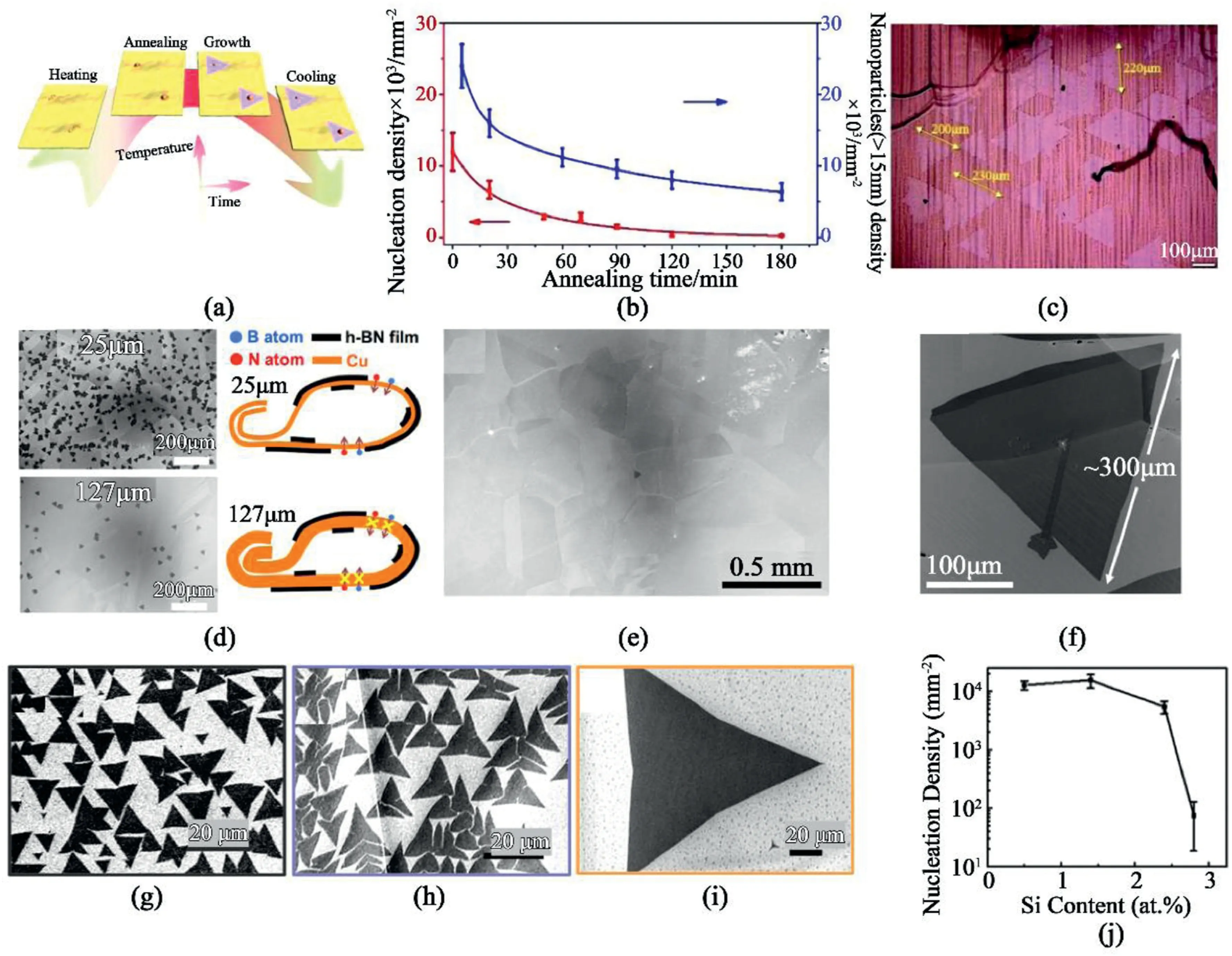
Fig.3.Enlarged hBN domain size in recent works.(a–c)Nanoparticle-assisted growth of large-size single crystalline h-BN.(a)Schematic of the oxidation nanoparticles assisting h-BN growth on copper foil.(b)Nucleation density of h-BN/large nanoparticles versus annealing time.(c)Optical image of the largest size h-BN[55].Reproduced from Ref.55with permission from the Royal Society of Chemistry.Copyright2018.(d–f)Growth of monolayer hBN using thick copper foil enclosure with inserted zigzag bent copper foil.(d)SEM images of h-BN grown on25μm/127μm Cu enclosure and the schematic of Cu enclosure.(e)SEM image of the growth with ultralow initial nucleation density<1per mm2.(f)SEM image of a large monolayer h-BN triangular domain[57].Reprinted with permission from Ref.57.Copyright2017American Chemical Society.(g–j)SEM images of the domains grown on Cu substrate doped with(g)≈0.5,(h)≈2.4,and(i)≈2.8at% Si.(j)Dependence of nucleation density on Si concentration in Cu substrate.Scalar bars are20μm[60].Reprinted with permission from Ref.60.Copyright2019Wiley-VCH.
3.Controllable synthesis
In recent years,much progress has been made to obtain the desired hBN crystals on various substrates under optimized conditions.The CVD growth of hBN is a complex process,affected by many factors including growth temperature,pressure,catalytic substrate,etc.Fine-tuning growth parameters allows the production of hBN grains or thin films of desired properties.In this section,we present a comprehensive investigation into the recent advancements made towards the controlled growth of hBN to regulate their domain sizes,grain orientations,morphologies,layer numbers,and stacking configurations.
3.1.Domain size
Limited domain size restricts applications of h-BN films.Enlarging the domain size of hexagonal boron nitride is challenging to obtain high quality film for numerous applications[48].In earlier stages,the domain sizes of h-BN grown on different catalytic substrates via CVD process,such as Cu[49],Pt[50],Co[51],Fe[52],were limited to several micrometers(Fig.2).So far,many attempts have been made to increase the domain sizes of hBN,and large-domain single-crystal hBN is obtained by controlling the nucleation density,similar to the graphene growth using chemical vapor deposition[53].
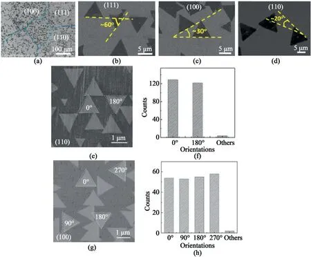
Fig.4.Correlation between substrate facets and the orientation of hBN films.(a–d)Orientation dependence of hBN triangles on Cu crystalline facet.(a)SEM image of the as-grown hBN on polycrystalline Cu foil.(b–d)SEM images of hBN grown on Cu(111),Cu(100)and Cu(110)with different orientations respectively[74].Reprinted from Ref.74by permission from Springer Nature,Nano research,Copyright2015.(e–h)Orientations of the h-BN domains distributions on Ge(110)and Ge(100).Friction force images of hBN domains grown on(e)Ge(110)and(g)Ge(100)with different types of orientations.Statistical distribution of the orientations of the hBN domains grown on(f)Ge(110)and(h)Ge(100),respectively[76].Reprinted with permission from Ref.76.Copyright2015Wiley-VCH.
The first strategy is to modify the Cu foil surface to reduce the nucleation density that leads to increased domain size.Cu foil was preoxidized in advance to control the nucleation density[54].The exposed catalytic surface area was reduced,resulting in a significant decrease of nucleation density.Therefore,the obtained hBN domain size was enlarged from1to20μm.Moreover,a nanoparticle-assisted strategy was reported[55].Larger oxidation-induced and smaller annealing-induced nanoparticles are the two main types of nanoparticles on the copper surface,and the oxidation-induced nanoparticles significantly influence the nucleation of h-BN subsequently for larger sized hBN grain growth(Fig.3a).The number of nanoparticles,and consequently the nucleation density could be further reduced by enhancing the extent of oxidation and annealing conditions(Fig.3b).Finally,the nucleation density was suppressed from~105nuclei per mm2to~102nuclei per mm2,so that the lateral length of a single h-BN single crystal could reach up to100μm(Fig.3c).Alternatively,a rational water-assisted chemical vapor deposition was first developed on the surface of liquid Cu[56].The water vapor introduced into the growth process could tune the hBN etching rate,nucleation density,shape and size of hBN with high growth reproducibility,resulting in large-sized single crystal domains of>330 μm.Water-assisted method requires precise control over the moisture level during the synthesis,thus limiting the reproducibility.Still,it is an efficient method to maintain the surface catalytic activity and control the hBN domain size by constantly removing the carbonaceous species on the metal surface.
The second strategy is to use Cu enclosure/envelop to limit the concentration of precursor and thus the nucleation density.Cu enclosure with Cu foil inside was employed as growth substrate instead of commonly used flat thin metal substrate[57].It is found that copper foil enclosure could suppress the diffusion of atomic species and reduce the nucleation intensity to~102per mm2(~103/mm2on25μm Cu foil),as shown in Fig.3d.Furthermore,the nucleation density is reduced by inserting a zigzag-bent copper foil into a copper pocket(Fig.3e).The synergy of the two strategies allows nucleation densities of less than1per mm2and sizes of~300μm single crystals(Fig.3f).The sizes of single-crystalline hBN domains were increased to7500μm2by CVD deposited on a Cu–Ni alloy substrate[58].
The third strategy is to use silicon doping sites on the metallic substrate,which also effectively reduces the density of crystal nuclei,and allow for the growth of larger hBN domains.The hBN was grown on a simple thin-film Fe/SiO2/Si substrate[59],in which Si acted as a transfer promoter in this growth process.Si diffusion into the Fe catalyst could be controlled by adjusting the thickness of SiO2,thus the nucleation density of hBN was reduced.With these innovations,the edges of obtained monolayer hexagonal boron nitride(hBN)single crystals reach up to300 μm and continuous hBN single-layer films consist of domain size over25 μm.When a small amount of silicon is introduced into the copper substrate,the morphology and nucleation density of deposited hBN can also be controlled reliably.Research indicated that the reduction of nucleation density of hBN could be reduced over two orders of magnitude by growing on Cu with Si,and the maximum lateral size of triangular domains reached up to0.25mm(Fig.3g–i)[60].These strategies of exploiting heterogeneous catalysts to control the nucleation density can be extended for the CVD growth of various2D material families,heterogeneous catalyst combinations,and the preparation of different reaction setups.
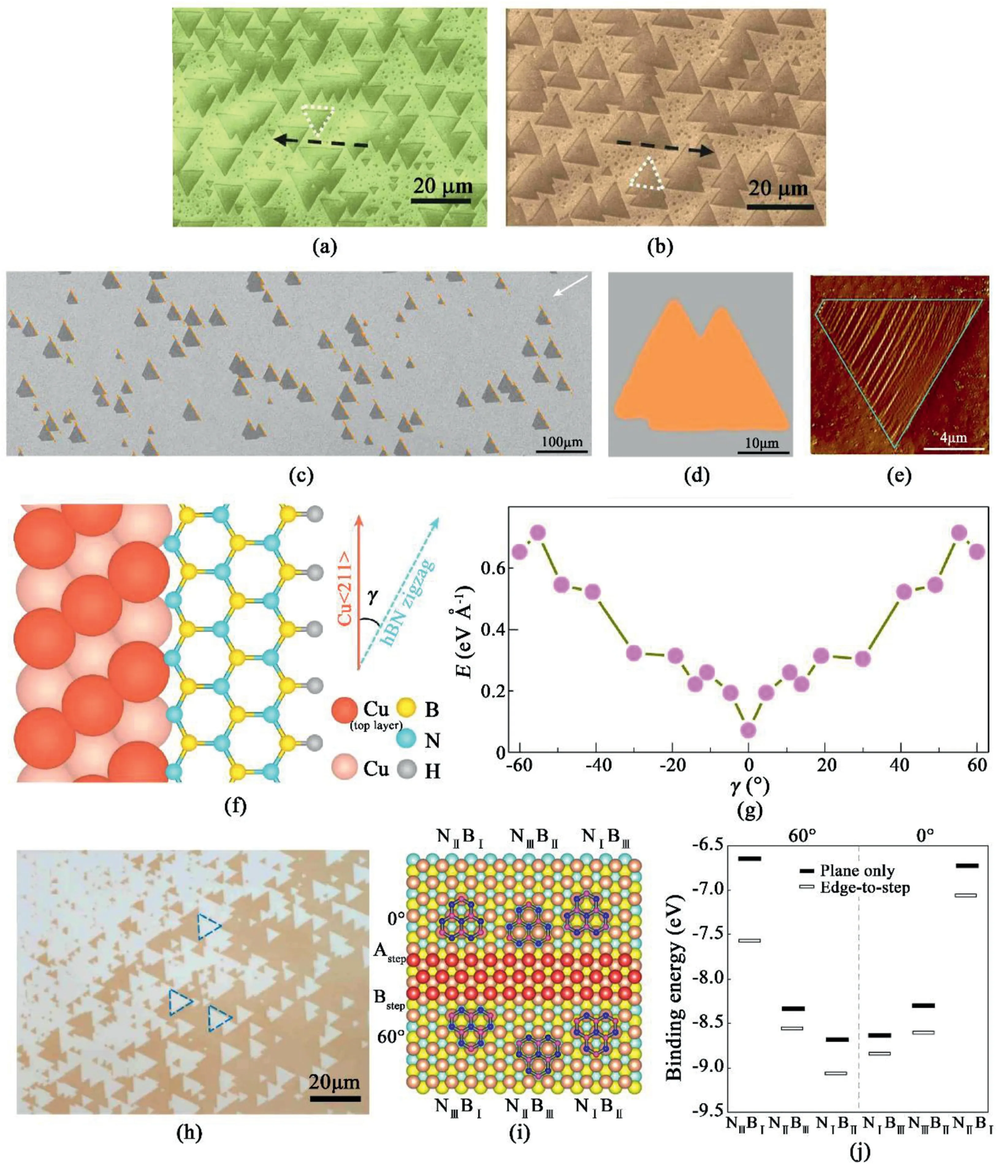
Fig.5.Orientated hBN on Cu substrates.SEM superimposed with EBSD maps of hBN triangles grown on(a)Cu(102)and(b)Cu(103)[77].Reprinted with permission from Ref.77.Copyright2016Wiley-VCH.(c–d)SEM images of unidirectionally aligned hBN domains on the Cu(110)substrate.(e)AFM phase image of a hBN domain on Cu(110).(f)Schematic diagrams of the configuration of the hBN lattice and the atomic step on Cu(110).(g)DFT calculations of the formation energies of various hBN edges attached to a Cu<211>step on the Cu(110)substrate[79].Reprinted with permission from Ref.79.Copyright2019Springer Nature.(h)mono-oriented hBN flakes on single-crystal Cu(111)films.(i)Lowest-energy atomic arrangements for six atomic stacking configurations.(j)Calculated binding energies for the six configurations by DFT[80].Reprinted with permission from Ref.80.Copyright2020Springer Nature.
3.2.Growth orientation
For constructing2D material-based electronics,continuous large-area h-BN monolayer film has been successfully synthesized via CVD[61,62].The orientations of2D film domains are found to benefit the electronic properties of devices[63,64].hBN nuclei,due to its polar structures,prefer to growing along at least two opposite orientations,so the obtained films are typically composed of random orientated h-BN domains.Different orientations introduce instability,severely damaging the performance of devices utilizing h-BN as dielectric[65].To obtain desirable material quality and device performance,the orientation and the distribution of the hBN domain are desired to be improved.If all the two-dimensional domains are in the same orientation,they may subsequently merge into a large single crystal layer.So far,various works have been attempted to study the mechanism of hBN orientations,so uniformly orientated hBN nuclei could merge into a single crystal films.
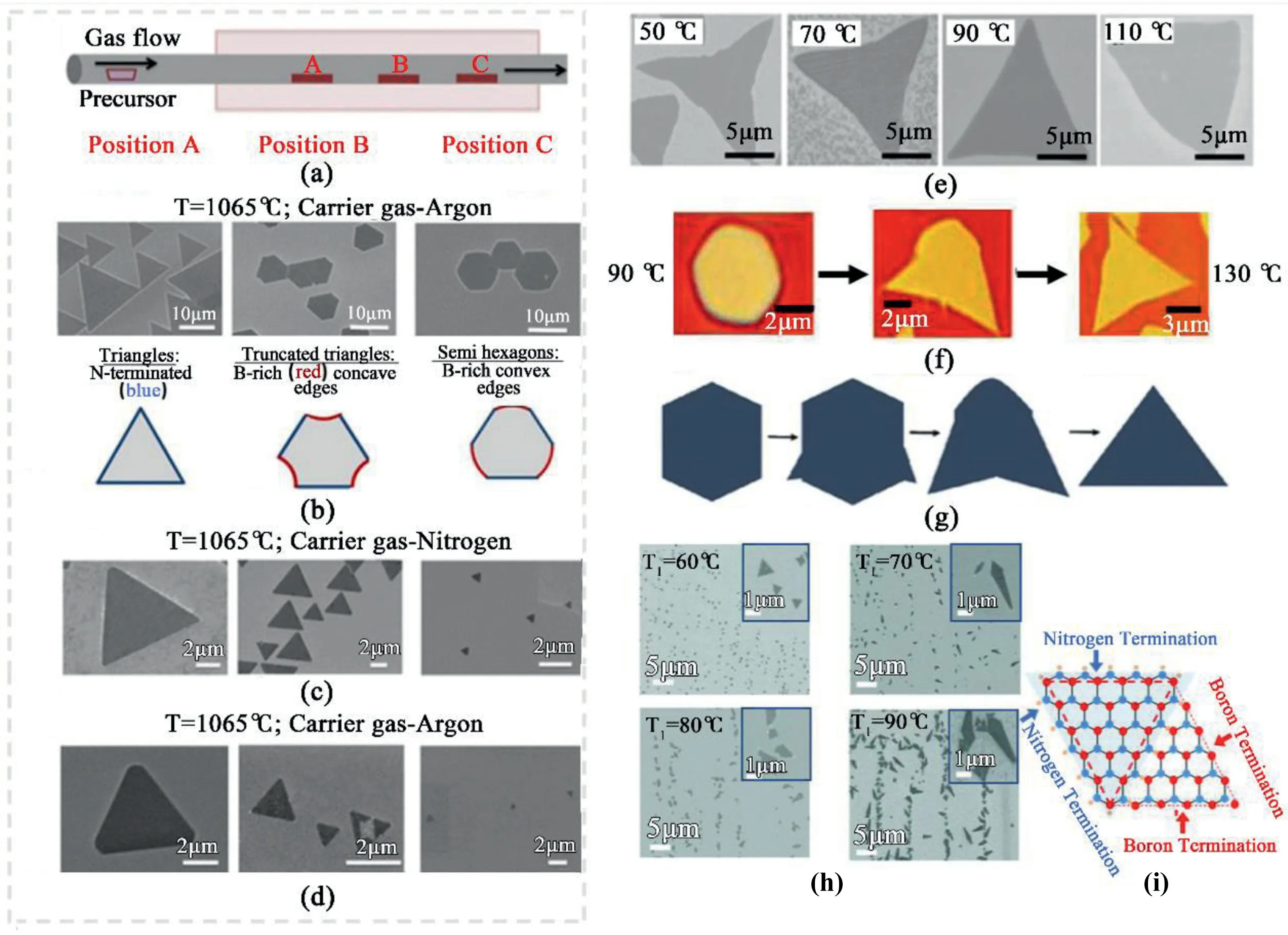
Fig.6.Morphology dependence on the concentration of precursor and active species.(a)APCVD experimental configurations.(b–d)SEM images of hBN crystals grown at different locations within the CVD reactor.(b)At1065°C with Ar carrier gas.Each image indicates the h-BN islands grown in position A,B,C in(a).(c)At 1065°C with N2carrier gas.Each image indicates the h-BN islands grown in position A,B,C in(a).(d)At1000°C with Ar carrier gas[85].Reprinted with permission from Ref.85.Copyright2015American Chemical Society.(e)SEM images of various-shaped h-BN domains grown on an annealed Cu foil surface under different belt heating temperatures of50,70,90,and110°C,respectively;scale bar=5μm[86].Reprinted with permission from Ref.86.Copyright2015Wiley-VCH.(f)Optical images of hexagonal crystal and corresponding evolution into the triangular domain as feedstock supply decreases.(g)Schematic representation of the transformation[87].Reprinted with permission from Ref.87.Copyright2016American Chemical Society.(h)SEM images of hBN crystals formed at precursor heating temperature of 60,70,80and90°C,respectively.(i)Schematic illustration of a diamond-shaped hBN[61].Reprinted with permission from Ref.61.Copyright2012American Chemical Society.
As hBN flakes grow epitaxially on catalytic metallic surfaces,the orientations of hBN domains are strongly coupled to the crystal facets of metal.Many works have attempted to synthesize hBN on polycrystalline metal substrates,such as Cu foil[66,67],Pt foil[68],and Ni foil[69].These polycrystalline substrate surfaces consist of variously orientated metallic grains which govern the growth of hBN films with different orientations.The hBN was also synthesized on single crystal metallic substrates,including Co(0001)[70],Ni(111)[71],Ir(111)[72].These works demonstrate that van der Waals(vdW)epitaxial growth on single crystal substrates could foster uniform orientations of hBN,and it is concluded that the orientations of the as grown hBN monolayer were determined by the underlying crystalline substrate facets[73].
The orientation of the hBN film is also strongly correlated to symmetry of the substrate facets(Fig.4a–d)as shown on several substrate facets including Cu(111),Cu(110),and Cu(100)[74].The orientations of the triangular hBN grains were further determined to be highly controlled on Cu(111)lattice,which pointed in two main directions[75].By studying the primary orientations of h-BN crystals grown on Ge(110)and Ge(100),it was proved that the strong correlation between the symmetry of the substrate crystal face and orientation exists not only in Cu,but also in those metallic substrates[76].The two-fold symmetry of Ge(110)provided two preferable orientations for the nucleation of hBN orientated along either0°or180°and for the fourfold symmetry of Ge(100)surface,the h-BN domains are identified to0°,90°,180°,and 270°orientations(Fig.4e–g).
The unidirectional epitaxy of h-BN monolayers is demonstrated to grow on Cu(102)and Cu(103)using chemical vapor deposition under low pressure(Fig.5a and b)[77].The symmetry axes of the h-BN nuclei were aligned in parallel with the underlying Cu substrate.Single-direction orientated hBN growth was also achieved on inclined Cu(101)surfaces,utilizing their strong vdW force between the h-BN.Wrinkles resulted from the relaxation of thermal stress are absent from the single-orientation domains[78].An edge-coupling-guided growth mechanism for mono-orientated hBN growth was raised(Fig.5c and d),revealing that one edge of the hBN triangle is parallel to the metal steps(Fig.5e)[79].Considering the lower symmetry of hBN,hBN growth was performed on a Cu(110)vicinal surface,on which the existence of surface steps reduces the symmetry of the substrate.These step edges contribute to the unidirectional alignment of hBN domains while each hBN single crystal can nucleate near the edge of the step.During the growth process,one edge of the hBN triangle adheres to the step edge and propagates rapidly on the platform between the adjacent step edges.Fig.5f illustrates the schematic of the configuration of the hBN crystal and an atomic step on Cu(110).γ is the angle between Cu<211>and the zigzag direction of a hBN crystals.From the DFT calculation results,the formation energy for hBN is the lowest at γ=0°(Fig.5g),which means γ=0°is a preferable orientation between the hBN crystals and Cu(110).Therefore,the coupling of Cu<211>step edges with hBN zigzag edges results in the mono-orientated hBN domain nuclei on Cu(110).Eventually singe-crystal hBN films over10×10cm2was obtained by this method.
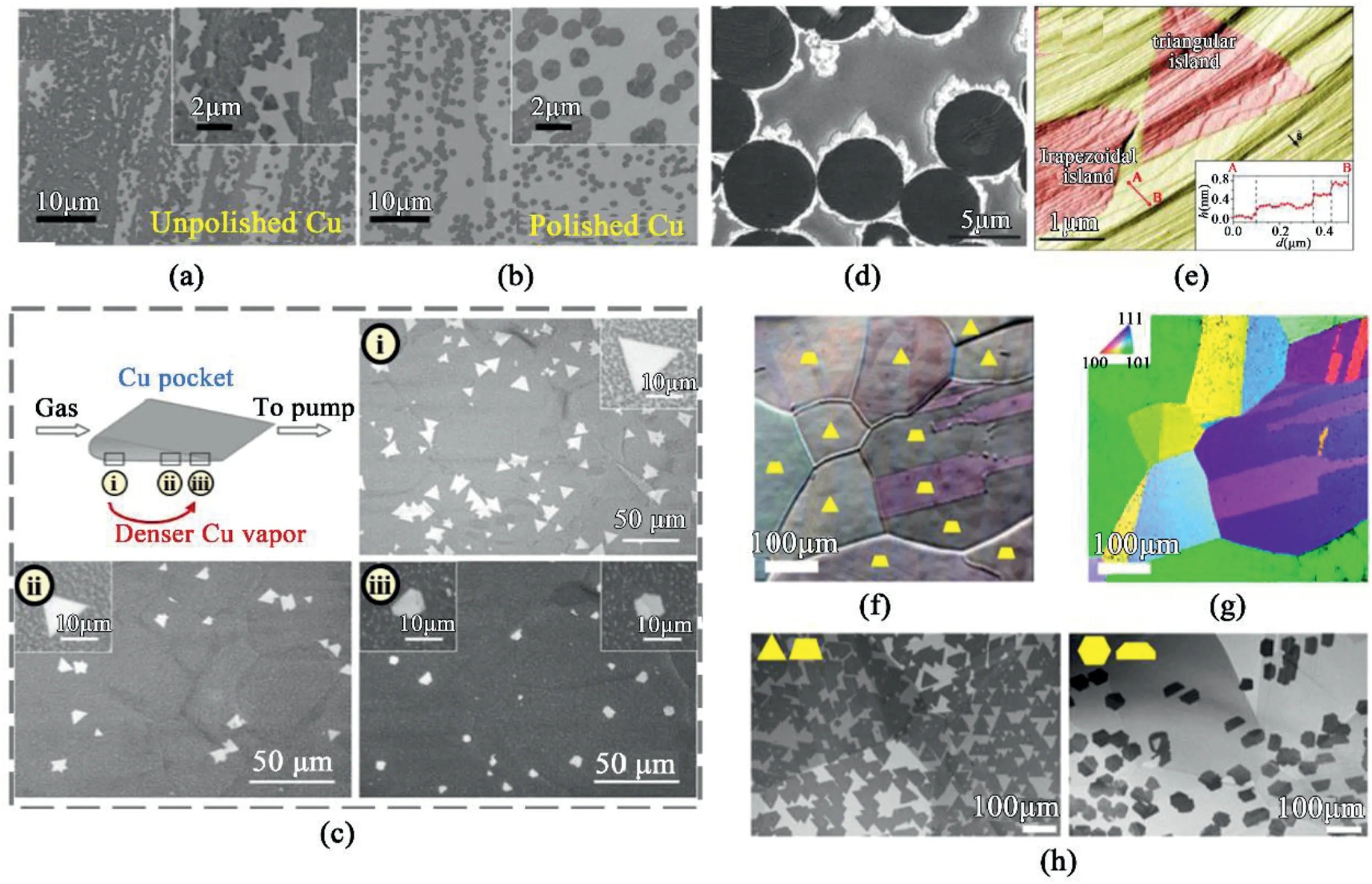
Fig.7.Substrate dependence of hBN morphology.(a,b)Comparison of hBN morphology grown on unpolished and polished Cu[66].Reprinted with permission from Ref.66.Copyright2014American Chemical Society.(c)Configuration of the Cu pocket and(c-i~iii)corresponding optical images of hBN grains at marked locations[88].Reprinted with permission from Ref.88.Copyright2015Wiley-VCH.(d)Circular hBN island-grown on liquid Cu[89].Reprinted with permission from Ref.89.Copyright2015Wiley-VCH.(e)AFM image of hBN islands(red)on Ir(111);Diagonal lines mark the step edges.The vertical dashed lines mark the position of Ir step edges[99].Reprinted with permission from Ref.99.Copyright2013American Chemical Society.(f)False color image of the same region labeled the hBN domain shape on each Cu grain.(g)EBSD map of the same region showing the Cu grain orientations.(h)SEM images showing the relationship between hBN shapes and Cu grains[57].Reprinted with permission from Ref.57.Copyright2017American Chemical Society.
It is previously believed that it is not likely to grow single-crystal mono-orientated hBN on Cu(111)because of its high-symmetry surface[77,79].However,mono-orientated hBN monolayers were successfully deposited on Cu(111)thin film(Fig.5h).[80]In this work,the importance of step edges in mono-oriented hBN crystals was further proved.For Cu(111),the mono-orientation of hBN monolayers is ensured by stronger adhesion of hBN to Cu(111)steps.DFT was utilized to simulate the binding energies of different stacking configurations(Fig.5i)to reveal the edge-to-step epitaxy effect.These binding energy differences indicate that the step edges on Cu(111)are essential to ensure mono-orientated growth of hBN crystals(Fig.5j).Additionally,Cu foil was annealed to eliminate the twin grains in Cu(111),thus unifying hBN crystals growth on the in-plane orientation.The optimized growth temperatures for mono-orientated hBN flakes ranges from995°C to1070°C in this work.
Growing hBN crystals with same orientation is important for obtaining high quality hBN films.These results provide feasible strategies regarding growing mono-oriented h-BN monolayers,which can also be applied into strategies for producing other2D materials.
3.3.Grain morphology
Intrinsic three-fold symmetry of the hBN microscopic lattice results in the hBN crystals growing into morphologies with three-fold symmetry[81].Further controlling the shape is essential for hBN reproducibility and applicability;however,it requires a thorough understanding of the intricate interplay of various parameters,growth mechanisms,and the thermodynamic stability of different configurations.While being structurally analogous to graphene,hBN exhibits a greater variation in the conformation of crystal termination edges as it contains two different atoms.Theoretical calculations on the free energies of various hBN edge energies have indicated the N-terminating zigzag triangular domain is the most energetically preferred configuration[81–83].Many experimental reports also attest to the calculation results of the tendency towards the formation of triangular islands with N-terminating zig-zag edges[84].
The strong correlation between the morphology and the ratio of boron to nitrogen active species concentrations,has been outlined by monitoring the APCVD growth of hBN on a Cu substrate[85].A gradual shift occurs,from triangles to truncated triangles,or to semi-hexagons along the CVD reactor with a decreased amount of active nitrogen species along the CVD tube(Fig.6a and b).When ammonia borane decomposes at high temperatures around1065°C,a large amount of inactive molecular nitrogen by-products forms,leading to an imbalance in boron and nitrogen active species along the tube.Hence,the ratio of boron-rich edges relative to nitrogen-rich edges becomes larger,with a more hexagonal crystal shape along with alternating B-and N-terminated edges.These hexagonal structures tend to adopt an irregular hexagonal shape,due to the different growth rate and different conditions on the edges.The shape evolution can be also explained by the Wulff construction,which is to achieve the equilibrium shape with minimum edge energy[66].The introduction of extra nitrogen into the reactor helps to keep the B:N ratio relatively constant along the CVD reactor tube;hBN crystals synthesized in positions A,B,and C are all in a triangular shape(Fig.6c).A lower reactor temperature at1000°C leads to decreased formation of inactive nitrogen by-products,propelling the formation of nitrogen-terminated triangular crystals at all positions along the CVD reactor.(Fig.6d)[85].
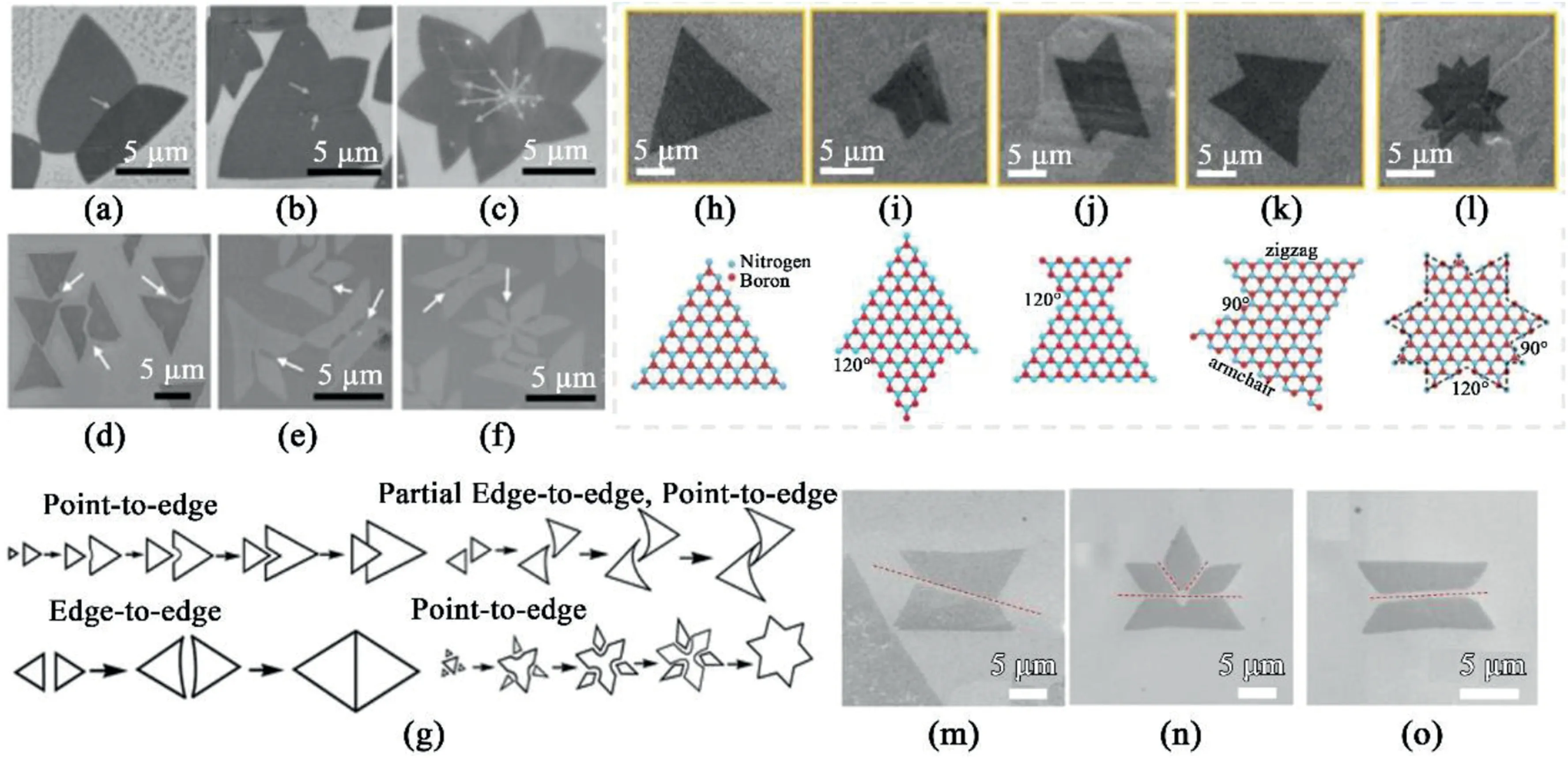
Fig.8.Complex structure from due to adjacent crystals and coalescence.Morphology development as adjacent fakes approach at proximity(a–c)SEM images of h-BN flakes with various complex structures.(d)SEM of closely-positioned h-BN flakes on Cu.(e,f)SEM images of lock and key structure formed before the complete merging of separate h-BN flakes.(g)The models for the dynamic merging process of h-BN flakes[86].Reprinted with permission from Ref.86.Copyright2015 Wiley-VCH.(h–l)SEM images corresponding schematic representation.(m–o)SEM images of polycrystalline grains with etched grain boundaries[88].Reprinted with permission from Ref.88.Copyright2015Wiley-VCH.
The correlation between morphology and the concentration of active species on the substrate has been investigated by changing heating temperature on the precursor.Higher precursor concentrations at higher heating temperatures lead to isotropic crystal growth,and forms symmetric hexagonal hBN[87].Meanwhile,a low precursor supply produces anisotropic growth,forming triangular crystal shapes.While a low feedstock supply leads to directional growth dynamics,an increase in the precursor supply induces more anisotropic growth to hexagonal hBN crystals.Fractal,branched,and negatively curved-hBN triangular domains engender upon further lowering the feedstock heating temperature.At higher concentrations,isotropic hBN grows into hexagonal to outward-curved edges(Fig.6e).Such transition implies the role of adatom surface diffusion kinetics in shape evolution[86].Reducing the precursor flow concentration by changing the precursor heating temperature during the growth allows the transformation of initially hexagonal crystal into triangular crystal,as shown in Fig.6f and g[87].Meanwhile,asymmetric diamond hBN domains are grown on Cu substrate at elevated ammonia borane heating temperatures(Fig.6h)[61].The stitching and convergence of equilateral nitrogen-terminated hBN triangles with boron-terminated hBN triangles form a diamond-shaped island(Fig.6i);however,the exact mechanism remains elusive.
Controlling the concentration of precursors determines the morphology by tuning the surface-adatom diffusion kinetics.However,other studies focused on varying the substrate proves adatom-substrate attachment kinetics is the main cause for driving the hBN grain evolution.hBN domains grown on unpolished and polished Cu exhibit hexagonal and triangular geometry,respectively(Fig.7a and b)[66].Surface oxygen species on unpolished Cu depress the edge-attachment energy barrier and prompt isotropic direction to hexagonal shape.Oxidized species on Cu substrates also dictate the morphology.While triangular hBN was preferred on the Cu substrate electropolished with 5–8V voltage,hexagonal hBN was preferred on Cu electropolished from 12to16V[57].Electropolishing leads to two major effects:1)smoothening of the substrate surface and2)increased oxidized chemical species(Cu2O,CuO and Cu(OH)2).The Smooth surface increases the Gibbs free energy barrier and increase surface diffusivity,lowering the nucleation density.Moreover,increased oxidation facilitates the dissociation of precursor gas and lowers the energy barriers for BN radicals to bond to both N and B-terminating edges.Consequently,the hBN domains grow into hexagonal geometry,while only N-terminated edges are preferred for hBN grown on unpolished Cu surface.Another study focuses on varying the Cu vapor concentration acting on different positions in the copper pocket.As Cu vapor concentration increases,hexagonal hBN domains are more favorably produced(Fig.7c)[88.].
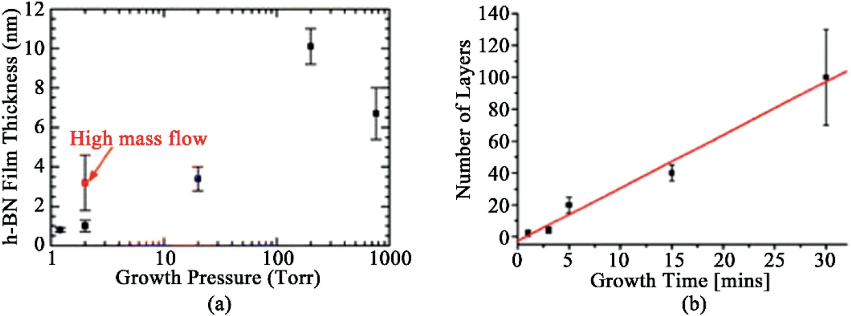
Fig.9.Layer Number dependence on various parameters.(a)hBN film thickness as a function of growth pressures[96].Reprinted with permission from Ref.96.Copyright2016American Chemical Society.(b)Number of layers as a function of growth time[98].Reprinted with permission from Ref.98.Copyright2012American Chemical Society.
CVD synthesis on a liquid Cu substrate promotes circular hBN domains with highly disordered N-and B-terminating edges(Fig.7d)[89,90].Smooth and uniform surface allows homogenous nucleation,adatom attachment,diffusion,and the isotropic growth towards circular hBN.Circular hBN domains,with disordered N-and B-terminating edges can be also correlated to seamless stitching at edges,and obtaining large-domain crystals.On the other hand,inherent step edges on concrete metal surface serve a crucial role in controlling the growth dynamics and the morphology[89].Due to the polar hBN zigzag edges and the electron density smearing at metal terraces,the hBN islands preferentially nucleate at the corners of the metal step edges.Subsequent growth of hBN on a metal substrate is also dictated by the adatom-metal step edge interactions.The energy required during the growth process system is modified on the substrate metal terraces[91].The synthesis of hBN on Ir(111)substrate has received much attention as Ir(111)substrate creates strongly periodic Moir´e pattern with hBN to give insight into electronic band structure.The synthesis of hBN on Ir(111)substrate using borazine revealed that the energies of hBN edges vary depending on the orientation of the metal step edge.Accordingly,the Ir step repositioning and the growth into a trapezoidal shape hinges on the relative orientation between hBN island edges and Ir steps(Fig.7e).Depending on whether the metal terraces are in step-up or step-down directions,the energies required for adatom attachment on the domain edges are different.The short bases of the trapezoidal hBN domains are facing towards step-up terraces of Ir substrate.The B and N radical species undergo charge redistribution at the densely packed atomic rows of Ir step edges.Hence,the hBN zigzag edges are strongly bound to the Ir steps.Thus,the hBN orientations are locked at the atomic edges,which preserves the domain evolution into equilateral triangle or parallel trapezoidal domains.The metal catalyst substrate orientation and the symmetry of the crystal shape also hold close relationship.False-color imaging of SEM images of the hBN islands(Fig.7f)shows different shapes are preferably grown on distinct areas of the Cu substrate.Further comparison with EBSD images(Fig.7g),evidences a symmetry-breaking effect;triangular or hexagonal domains are procured on highly symmetric Cu(111)and Cu(100),while trapezoidal or less-symmetric shapes are rendered on Cu(101)(Fig.7h)[57].
Multiplex architectures are often attained,as adjacent crystals either coalesce or compete for adatoms during the growth.The dynamic merging models,referred to as point-to-edge and edge-to-edge merging,are studied[86].(Fig.8g)When two growing hBN flakes come into proximity,the adatom diffusion to the tip of the flake occurs at a faster rate than that to the edge of the straight edge of the hBN flakes,leading to an inward-curved edge.In point-to-edge mode,the edges curve towards a negative direction,while the other two edges of the same BN flakes remain intact.Edge-to-edge merging involves both edges of hBN flakes becoming negatively curved while others remain unchanged.Hence two adjacent flakes initially display a lock-and-key structure of intruding crystal and negatively curved edge.Further growth of the adjacent island yields a variety of complex structures(Fig.8d–f).
Seamless stitching on the grain boundaries of the merged flakes on a solid metal substrate is hard to achieve due to the disparity in the terminating edges’polarities.Hence,these converged crystals consist of defect lines(Fig.8a–c)[86,92,93].The combined crystals adopt a variety of polygonal shapes depending on the angle of the junction of the converged domains(Fig.8h–l)[92–94].The stitching of two mirroring triangular domains is the most commonly observed among the various polygons reported.These merging crystals are often in mirrored directions,tilted at0°,30°,and60°.Fig.8m–o shows the SEM image of two adjacent domains approaching each other,with mirrored reflection at various angles[88].Thus,the domains exhibit trapezoidal,or even a‘crown-like’shape,formed by different domains intersecting at different angles.Considering the orientation dependence of the domains forming on the same plane,the intersecting edges at0°and60°involve both N-terminating zigzag edges;while those intersecting at30°and90°involve one of the domains with an armchair edge.
3.4.Layer number
The synthesis of multilayer hBN is crucial towards its application in real devices and eliciting new properties engendered by modified electronic properties[95].Controlling the number of hBN layers is another daunting task due to the layer number dependence of the optical bandgap[96],and second-harmonic generation for odd-numbers of hBN layers[36].However,due to the electronegativity difference between B and N and reduced resonance stability of hBN,both in-plane and interlayer electrostatic interactions of hBN are enhanced.As in-plane growth is more favorable than vertical growth,fine synthetic control over the layer number thickness has not been fully realized so far[97].However,several studies still attempted to outline the relationship between a few synthetic parameters and their contribution towards the controlled synthesis of multilayer hBN.
The relationship between the layer number and CVD chamber pressure has been explored.At constant temperature under Ar/H2carrier gas flowing with ammonia borane precursor,an increase in the pressure results in an increase in the number of hBN crystal layers.Varying the temperature serves as a simple method for controlling the pressure of the precursor species.As the pressure increases,the growth rate increases,producing a thicker layer of hBN crystals.The linear relationship between the pressure and hBN film thickness is halted when the pressure is increased near atmospheric pressure.At higher pressure,the O2etching plasma interferes with the hBN growth on the system,thereby slowing the chemical reaction and reducing the thickness of the hBN film(Fig.9a)[96].
The layer number also possesses a positive relationship with the concentration of the precursor gas.The concentration of borazine within the CVD reactor was tuned by changing heating temperature on the borazine precursor of APCVD with Pt as a substrate[95].Unlike graphene adlayer growth,which is dictated by the precursor decomposition[99,100],the vertical growth of hBN tends to be independent of the reaction time.Due to the high reactivity of hBN edges,decomposed borazine species prefer lateral growth into a continuous film[95].hBN films were prepared on Ni substrates by optimization of growth temperature,growth time,and precursor temperature[100].At1000°C,prolonging the growth duration and denser precursor flow increases the number of layers;the vertical growth is still limited to a few layers.However,a growth temperature higher than1000°C tends to yield a bulk hBN film formation,even with a reduced growth duration.Meanwhile,another hBN CVD synthesis study performed at constant low pressure indicates a linear dependence of the number of hBN layers on the growth time(Fig.9b)[98].
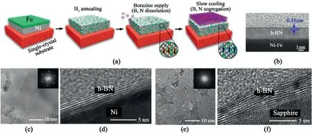
Fig.10.Substrate-dependent multilayer hBN synthesis(a)Schematic of the CVD growth of multilayer hBN on a Ni–Fe alloy film catalyst.(b)Cross-sectional TEM images of the as-grown hBN on the Ni–Fe/spinel(100)[102].Reprinted with permission from Ref.102.Copyright2018American Chemical Society.(c–f)HRTEM comparisons on MOCVD grown:(c)In-plane view and(d)Cross-sectional view of hBN grown on Ni(111)(e)In-plane view and(f)Cross-sectional view of hBN grown on sapphire[105].Reprinted from Ref.105from MDPI,Open Access.
Apart from the optimization of CVD-reactor parameters,the substrate condition was modulated to foster multilayer synthesis.Slow cooling of the Fe substrate after the growth has yielded hBN films from5to15nm thick by allowing the segregation of boron and nitrogen from the iron surface[101].Varying the amount of ammonia borane precursor under the controlled precursor heating temperature confirms the multilayer growth process as a defect-mediated growth,on which the adlayers form by utilizing the initial layer as a template for growth.Unlike monolayer hBN,multilayer hBN exhibits a particle-like defect structure on its underlying monolayer hBN.This defect point serves as a nucleation site for the adlayers.Hence,adlayers share a common geometric center[57].
A Ni–Fe alloy as a metal substrate and byproduct-free borazine as a precursor were adopted to synthesize large,highly-crystalline,and uniform multilayer hBN[102].(Fig.10a).The Ni–Fe alloy offers an avenue with similar B and N solubility,thus prompting uniform segregation and formation of multilayer hBN lying flat on top of each other(Fig.10b).On the other hand,the inert sapphire substrate was also selected to produce 2–6homogeneous layers of hBN sheets in the LPCVD setup[103].Sapphire substrates,due to the absence of a catalytic surface,facilitate adlayer growth on the previous layer,in contrasts to metal substrates that generally yield continuous monolayer hBN.Moreover,as sapphire provides a platform for epitaxial growth of the hBN islands,wrinkle-free multilayer hBN forms with single and strict AA’stacking configurations[103,104].
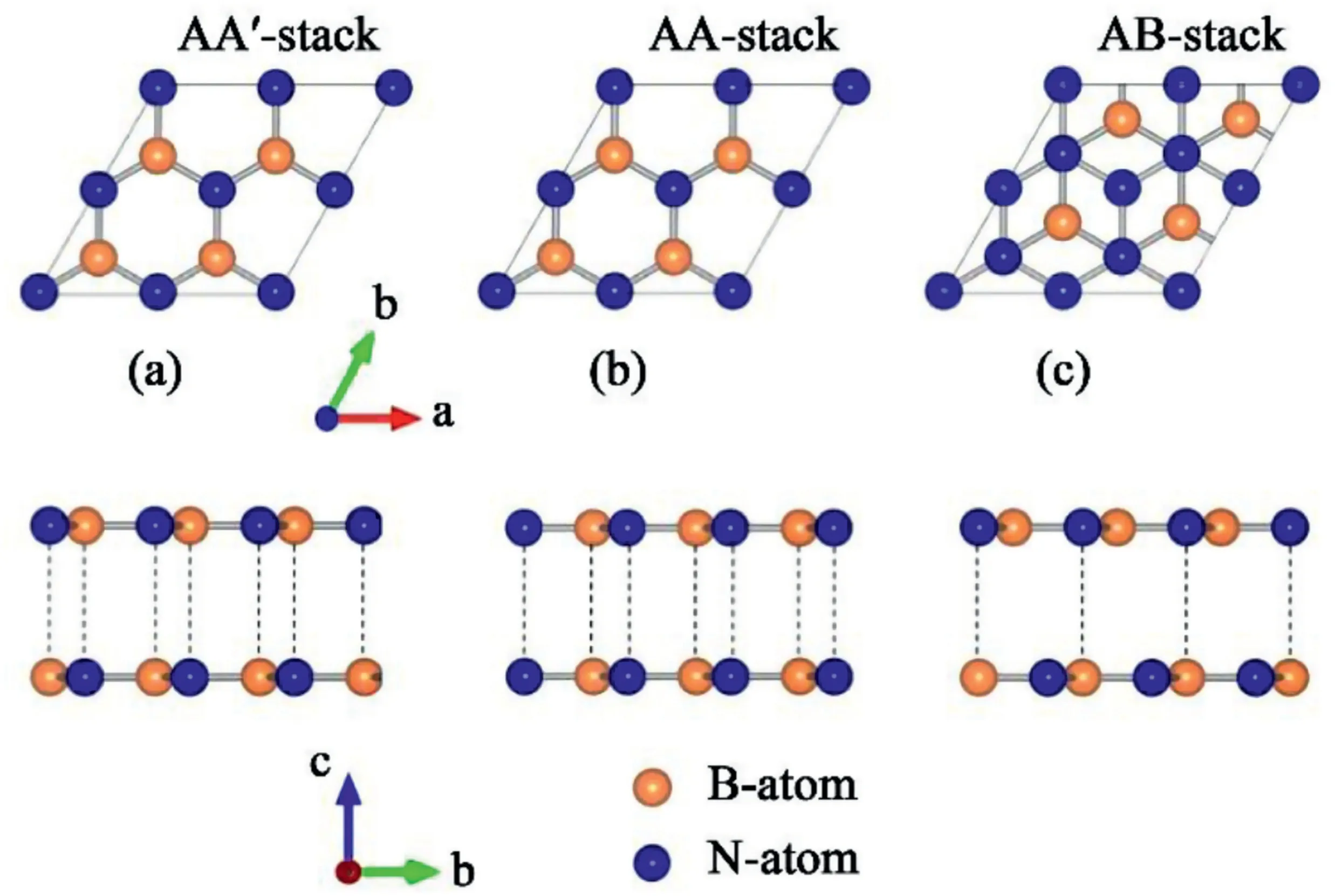
Fig.11.Schematic of three major stacking configurations in bilayer hBN,categorized by interlayer rotation and shift.(a)in AA’configuration,two layers are anti-aligned so that B is on top of N and N is on top of B(b)in AA configuration,B is directly stacked on B and N is directly stacked on N of the adjacent layers(c)in AB configuration,one layer is translated by a single bond length.B lies on top of N of the underlying layer[112].Reprinted figures with permission from Ref.112.Copyright2019by the American Physical Society.
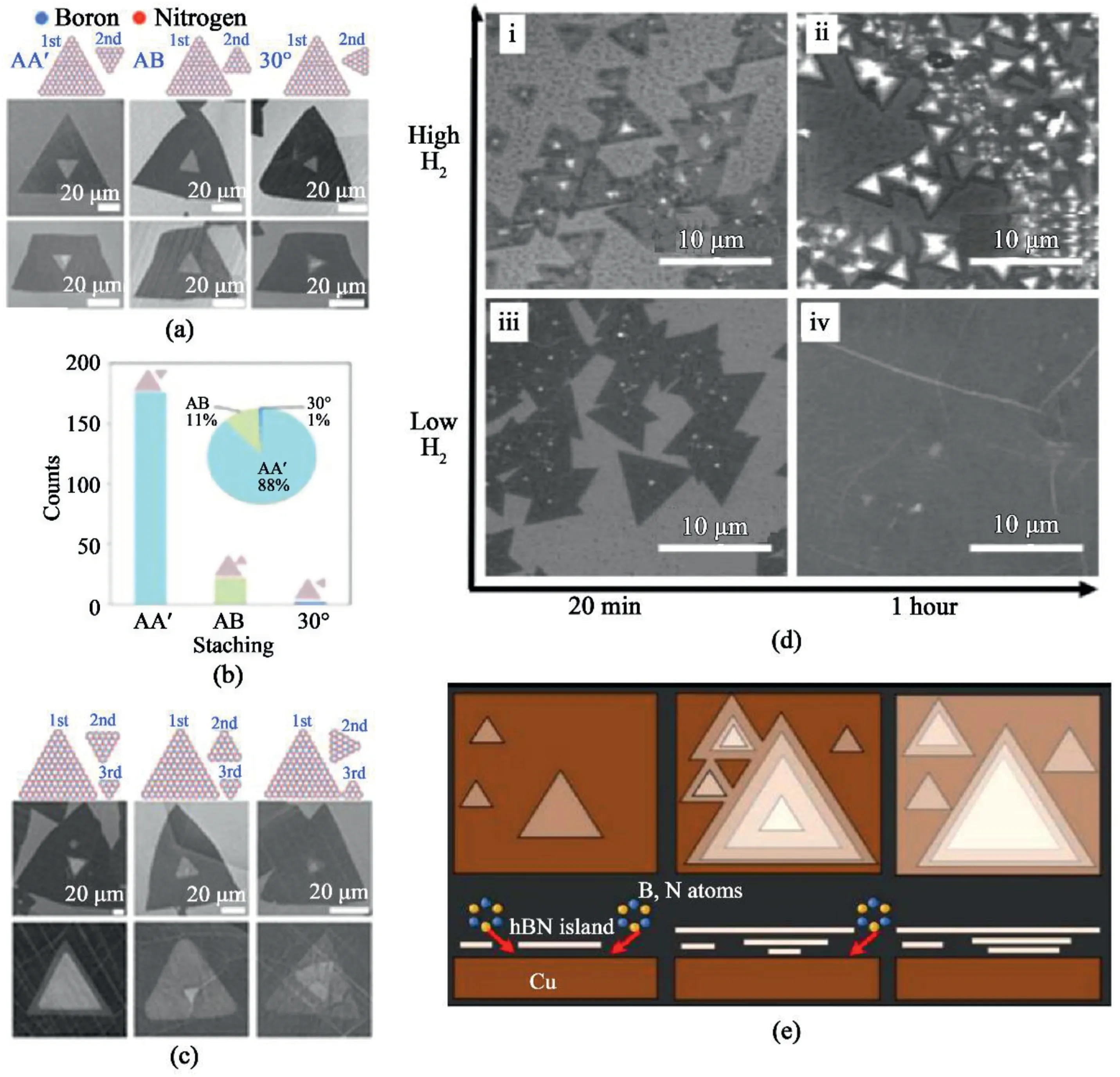
Fig.12.Growth of bi-and tri-layer hBN domains.(a)Schematic of the atomic structure and SEM images of AA′,AB,and30° twisted stacking configurations.(b)Statistical analysis of three bilayer-stacking configurations.(c)Schematics of atomic structure and SEM images of tri-layer stacking configurations[57].Reprinted with permission from Ref.57.Copyright2017American Chemical Society.(d)SEM images of multilayer hBN crystals grown on Cu with varying times and hydrogen flow.(i)20-min growth with200sccm H2.(ii)2-h under200sccm H2.(iii)20-min growth with20sccm H2.(iv)1h with20sccm H2.(e)Schematic illustration of growth mechanism for Bernal-stacked hBN[113].Reprinted with permission from Ref.113.Copyright2019IOP Publishing.
Metal-Organic CVD(MOCVD),which allows controlled introduction of precursor gases,has been widely adopted in synthesizing multilayer hBN.Triethylborane and ammonia precursors under H2carrier gas flow are introduced for the synthesis.hBN growth using conventional CVD is limited with the decomposition of molecular precursors,leading to a stoichiometric imbalance between B and N active species and the extent of metal substrate exposure.Hence,MOCVD allows the synthesis of homogeneous few-layer hBN not only on metallic catalysts but also on noncatalytic substrates such as sapphire[106],SiC[107],and insulating nitrides[108–110].While direct synthesis on non-catalytic substrates enables facile device construction method without additional transfer,it results in a hBN layer with low crystallinity and layer inhomogeneity.However,the catalytic metal substrate does enhance the quality and homogeneity of multilayer hBN[110].Owing to the catalytic adsorption and decomposition on the metallic surface,the resulting hBN multilayer films exhibit higher crystallinity and homogeneity(Fig.10c–f).
Furthermore,a closer inspection of hBN layer stacking on Ni(111)has been conducted[105].At the initial stage,surface catalytic reactions govern the hBN growth.As the number of hBN layers increase,the catalytic Ni surface is passivated,and adlayer growth is governed more by the defect impetus,hence the misalignment among respective layers with increasing growth time.
3.5.Stacking order
The stacking sequence and stacking mode of hBN layers have drawn tremendous attention due to the altered symmetry characteristics and atomic orbital overlapping.Hence bilayer to multilayer hBN possesses disparate electronic and luminescent properties depending on their stacking sequence and stacking fault configurations[111].Fig.11presents major stacking configurations that occur in bilayer hBN[112].Unlike graphene,hBN generally adopts AA′stacking sequence,as demonstrated in numerous multilayer hBN synthesis procedures[98,101,103,104].AA′stacking,with the lowest formation energy,is formed by the rotation of successive layers at60°that all nitrogen lies above boron and all boron lie above nitrogen.AA′stacking mode serves as a good insulator,dielectric material,and membrane for proton exchange membranes[98,101,103,104].It was reported that AB stacking also has similar stacking energy to AA’stacking[111].AB stacking is formed by translating one layer by a single bond length(1.4Å)to stack N to B[113].AB stacking mode is also noted for strong second-harmonic generation[114]and magnetoresistive effects at the edges[115].
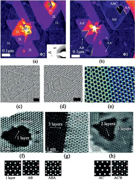
Fig.13.Multi-layer hBN domains and boundary edge of different stacking faults.False-color DF-TEM of triangular,few-layer hBN domains.(a)Accounts for layer numbers.(b)Accounts different stacking structures.(c,d)HRTEM images of AA′and AB′stacked TEM.(e)False-color HRTEM image of stacking boundary of ABA/AA’A stacked film[116].Reprinted from Ref.116from AAAS,Open Access.(f–h)FT-filtered HAADF-STEM images and simulated pattern of(f)hBN nanosheets showing bi-layer surrounding a monolayer region.(g)Trilayer region adopts ABA stacking order.(h)Bi-tri-layer region.The bi-layer adopts AC’,and the tri-layer is AC’B stacked[117].Reproduced from Ref.117with permission from The Royal Society of Chemistry.Copyright2016.
The synthesis mono-,bi-,and tri-layer hBN and AA’,AB,and30°twisted interlayer stacking were also reported[57].Fig.12a and c shows numerous bi-and tri-layer hBN and the different stacking configurations exhibited in different structures.Under their synthetic scheme,the AA′-mode prevails compared to the AB or30°interlayer stacking(Fig.12b).Additionally,the stacking mode between bi-and trilayer hBN strongly depends on the relative rotation between the monolayer and bilayer,which has been well demonstrated(Fig.12c).
The AB-stacking configuration of hBN on Cu and Fe substrates was deliberately controlled by maintaining high growth temperatures and incrementally adding hydrogen during the growth[113].At elevatedtemperatures,each layer slides and rearranges into AB-stacked configurations.A high concentration of hydrogen gas etches the edge of the hBN crystal during the growth,leading to the formation of multi-layered adlayers on the hBN crystals(Fig.12d–i and12d-ii).Meanwhile,hBN crystals merge into a continuous film with increasing growth time and low H2flow(Fig.12d–iv).Fig.12e displays the schematics of the growth process.The precursor gas adsorbs onto or dissolves into the metal to form ad-layers below the first layer,each adlayer nucleates at a common seeding point of the metal catalyst.The growth of the adlayers is halted as the hBN film reaches full coverage.
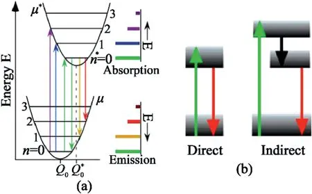
Fig.14.Single photon emission mechanism illustration.(a)Configuration coordinate diagram showing phonon-mediated transitions.(b)Two energy levels diagram showing the direct(left)and indirect(right)excitation mechanisms of SPEs[128].Reprinted from Ref.128with permission from American Physical Society.Copyright2017.
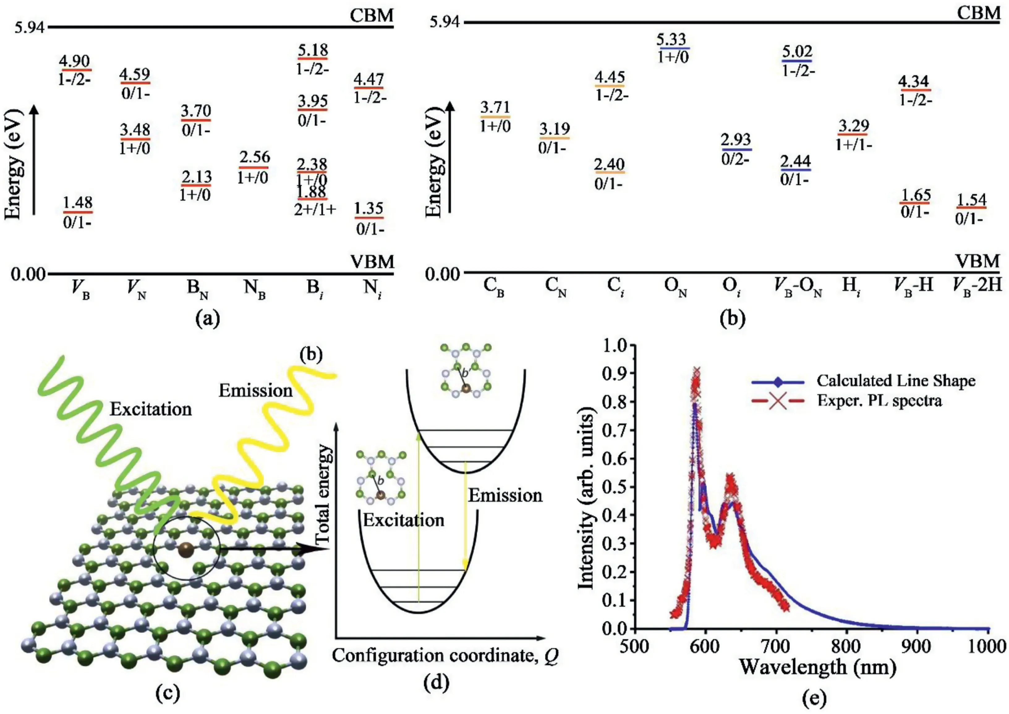
Fig.15.Simulated results of defects in hBN responsible for SPEs.(a)and(b)Charge state transitions of different point defects in hBN[135].Reprinted figures with permission from Ref.135as follows:L.Weston et al.,Physical Review B,97,21,2018.Copyright2018by the American Physical Society.(c)Schematic of a CBVN defect and its excitation.(d)Schematic of one-dimensional configuration coordinate diagram showing photoluminescence process,where b and b’refer to the length of C–B bond in the ground state and excited state[132].Reproduced from Ref.132with permission from The Royal Society of Chemistry.Copyright2017.(e)Calculated and experimental PL spectra of CBVN defect[138].Reprinted with permission from Ref.138.Copyright2014IOP Publishing.
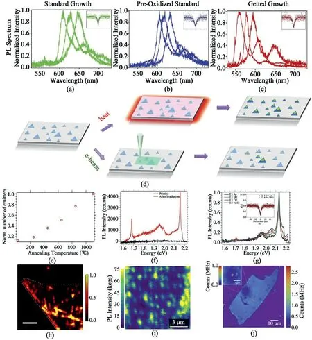
Fig.16.Different strategies to generate SPEs in hBN.Photoluminescence spectra of hBN grown by(a)standard growth,(b)pre-oxidized growth,and(c)gettered growth method[141].Reprinted with permission from Ref.141.Copyright2019Wiley-VCH.(d)Schematic of SPEs generation by thermal annealing and electron beam irradiation.(e)Normalized number of emitters in hBN as a function of annealing temperature.(f)Representative PL spectra of SPEs in hBN generated by e-beam irradiation.(g)PL spectra of an SPE after sequential annealing in argon,hydrogen,oxygen,and ammonia gas[137].Reprinted with permission from Ref.137.Copyright2016American Chemistry Society.Confocal PL map of(h)hBN flakes after electron irradiation[142],Reprinted with permission from Ref.142.Copyright 2018American Chemistry Society(i)hBN SPEs arrays generated by the focused ion beam[143],Reprinted with permission from Ref.143.Copyright2019American Chemistry Society and(j)SPEs induced by blisters[144].Reprinted from Ref.144,Copyright2020,with permission from Elsevier.
Synthesis of multilayer hBN demonstrates the presence of both AB and AA′stacked multilayers on monolayer hBN with common orientation and stacking boundaries at the edge of two different stacked islands.The combination of DF-TEM and HRTEM substantiates the presence of both AA′and AB stacked layers(Fig.13a and13b).The triangular defects are present in the same direction in AB-stacked hBN while occurring in opposite directions in AA′stacked hBN layers(Fig.13c and13d).The false-color HRTEM image in Fig.13e displays AA’A and ABA-stacked hBN islands stitched together perfectly,forming a sharp stacking boundary in a zigzagging pattern.These atomically sharp twin boundaries at AA’/AB stacking boundaries exhibit a reduced bandgap and conducting behavior,offering prospects towards the formation of a onedimensional electron channel within insulating hBN multilayers[116].
While AA′and AB are the most common stacking configurations reported,CVD growth at high temperatures leads to elevated kinetic energies of individual atoms.Hence,the B–N electrostatic interaction can be suppressed,and nanosheets can readily adopt alternative stacking configurations[117].Furthermore,APCVD allows growing2–3layers of hBN using ammonia borane as a precursor on liquid Cu/W substrate.The acquired hBN nanosheets manifest AB,ABA,AC′,and AC’B configurations,which have higher energies than AA′stacking mode.Fig.13f–h validate well-corresponding FFT-filtered HAADF-STEM images with the simulated images that confirm the synthesis of various stacking conformations[117].
Table1presents a summary of synthesis parameters and resultant characteristics of CVD-grown hBN.Hence deliberate modifications of the growth parameters allow optimization the resulting h-BN islands.
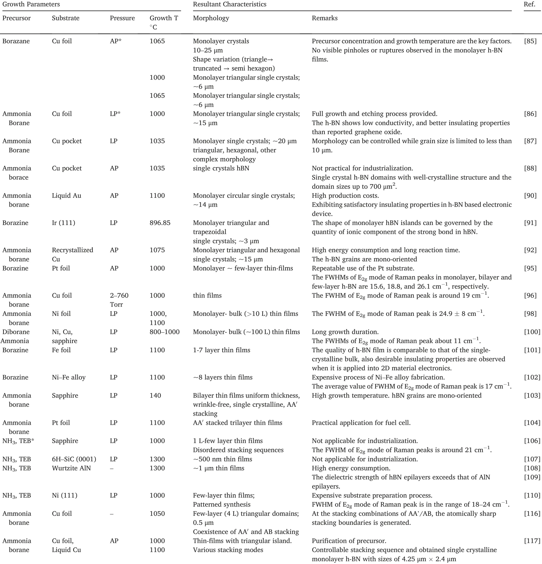
Table1 Summary of the hBN CVD growth parameters and resulting crystals.
4.Single-photon emissions in hBN
Single-photon sources are of great significance for quantum communications,quantum computation,and quantum metrology[118,119].SPEs have been discovered in many materials such as atoms[120],quantum dots[121,122],the color center in diamond[123–125],etc.However,in these systems,the generated SPEs suffer from various disadvantages,including low quantum efficiency,poor scalability and integrability,and instability.hBN has recently attracted vast amounts of research interest in its applications for SPEs due to its stability at room temperature[126],with its2D nature to be integrated into chips and its flexible tunability[127].
The SPEs come from the point defect sites in hBN.Upon excitation,the electron is excited to the excitation state from ground state and emits one photon when goes back to ground state.As shown in Fig.14a and b,the excitation-emission process may be accompanied with phonons[128].It was reported that when the energy difference between the exciting light and ZPL of the SPEΔE=Eexc-EZPLis smaller than200meV,the SPEs generation follow a direct excitation mechanism.Conversely,if ΔE is larger than200meV,it’s more likely to be an indirect excitation mechanism that may be accompanied with an intermediate electronic state from the defect or from a neighboring defect,which subsequently causes the misalignment of the absorption and emission dipoles.
In the following section,we review some recent work discussing the origins of SPEs in hBN,some strategies to tune the emissions in hBN and several trials to apply SPEs in hBN into realistic applications.
4.1.The origins of SPEs
Even though many studies have proved the existence of SPEs in hBN layers or bulk crystals,there is still no direct experimental evidence to reveal their origins.However,plenty of efforts have been made from a theoretical simulation perspective[129–133].Typically,the deep energy levels are generated from point defects in hBN such as boron vacancies(VB)and nitrogen vacancies(VN).Defects may also form if other atoms are substituted in for boron or nitrogen atoms.For example,if a boron atom is replaced by a nitrogen atom,then the defect is normally labeled as NB,and other defects can be labeled similarly as BN,CB,CN,etc.Moreover,if a defect is labeled as VNCB,it refers to a nitrogen vacancy with a neighboring boron atom replaced by a carbon atom[134].
DFT calculation was utilized to calculate the charge state transition levels and formation energies of native vacancies,anti-site defects and atom contaminate(carbon,hydrogen,and oxygen)induced defects[135].Fig.15a and b summarize the calculated results of the charge state transitions levels of different point defects in hBN that lie within the bandgap.With the Fermi level elevation,the defects are stabilized with increased charges.For example,when the Fermi level increases,VBis stabilized into a1-charge state and then further to a2-charge state.Meanwhile,the formation energies of these defects were also calculated,which showed that the isolated native defects in hBN have high formation energies and thus are not thermodynamically stable without exotic atoms.The presence of hydrogen or oxygen helps to stabilize the boron or nitrogen-vacancy defects.It was also speculated that CBwas the possible emission source for the4.1eV emission line rather than CNdefect,while for SPEs around2eV,the interstitial defects Nior Bior their complexes may be the emission centers.
Another research group also conducted DFT in order to calculate the atomic structures and corresponding zero phonon lines(ZPL)to figure out the emission origins of SPEs[132].To obtain a reasonable results list,three criteria were applied:i)the positions of defect levels should be within the band gap while not being close to the bulk bands;ii)the optical spectrum should be polarized as revealed from reported experimental results[126];iii)the energy of the zero phonon line should be between1.3eV and2.0eV which covers the range of reported ZPL energies[126,136,137].Combining the screening results and the calculated Huang-Rhys factor as1.66,it was found that the CBVNdefect,as shown in Fig.15c and d,is a potential candidate as an emission site.Similarly,based on the first-principles simulation results,the SPEs at 2.0eV may also be attributed to the CBVNdefect[138].The simulated photoluminescence spectrum matches well with the experimental results(Fig.15e).Additionally,other kinds of defects including dangling bonds[133],VNNB[139],VBCN[130]were also speculated to be responsible for SPEs in hBN,however direct experimental evidence is still needed.
4.2.Generation and tuning of SPEs in hBN
Efficient generation of SPEs in hBN has been regarded as a hurdle to overcome among researchers.The emission wavelengths of generated SPEs can vary from ultraviolet to near-infrared[140].Typically,point defect formation strategies can be grouped into two categories:pristine defect formation during hBN growth and post-treatment of as-grown hBN.An approach was reported to control the boron diffusion into growth substrates for desired SPEs[141].During the growth process,boron diffusion will induce strain in Cu due to the lattice expansion and subsequently modify the defect formation.By comparing normal Cu,pre-oxidized Cu,and normal Cu on a Ni plate,it was possible to regulate the formation of specific defects in hBN with distinct spectral regions as shown in Fig.16a-16c.The SPEs of hBN grown on normal Cu and pre-oxidized Cu mostly located in the range of600–650nm.Owing to higher boron solubility in Ni medium,large amounts of boron atoms can be gettered into the Ni plate when Ni is used as Cu support.Consequently,as-grown hBN on Cu/Ni presents different types of defects compared to those grown in other conditions,shifting the SPE emission wavelength to 550–600nm.
Normally,the SPEs in pristine hBN are not only unstable but are also deficient in number.Several works focus on the post-treatment of hBN to surmount the limits of intrinsic hBN properties.Thermal annealing and electron beam irradiation were proposed to engineer the SPEs in hBN[137].Fig.16d shows a schematic of these two methods.The number of generated emitters increased with the increasing of annealing temperature(Fig.16e).Moreover,these generated SPEs were quite robust,which was proven by the maintained PL spectra after sequential annealing in argon,hydrogen,oxygen,and ammonia gas(Fig.16f and g).It was also noted that the SPEs generated by these two methods could be classified into two groups with similar local phonon energies,indicating that they might have similar crystal structures.High energy electron irradiation was also utilized to generate SPEs in four kinds of exfoliated hBN flakes[142].Electron irradiation can either generate new defects or activate the existing defects in hBN.The emitter densities increased dramatically in all samples and were distributed throughout the entirety of the flakes.An example is shown in Fig.16h.Inspired by the results that the quantum emitters could be formed at edges,which may result from more dangling bonds,hBN arrays were constructed with large amounts of exposed edges by using a focused ion beam(FIB)[143],sufficiently generating SPEs in the hBN arrays as shown in Fig.16i.The SPE generation reached the highest yield near the smoothly milled holes on unwrinkled hBN.Meanwhile,blisters in hBN can also be a substantial option for SPE generation as it can provide local strain in2D materials(Fig.16j)[144].Surprisingly,the generated SPEs were quite stable and could maintain the quantum emitting performances without blinking and bleaching for a year,even under different pressures.In addition,laser irradiation[145]and plasma treatments[146]are also feasible ways to generate SPEs in hBN.Generally,the generation of the SPEs in hBN focuses on the introduction or modification of local defects in hBN by sufficient means.
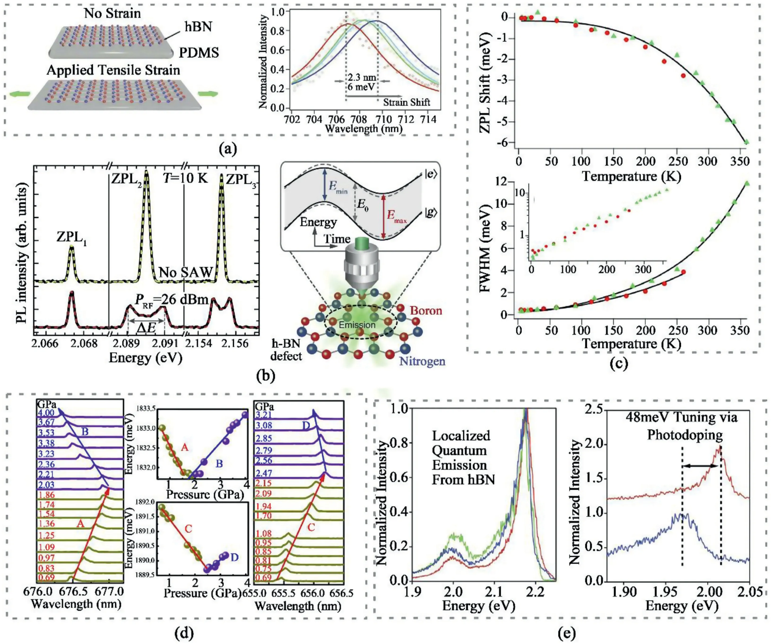
Fig.17.Different strategies to tune SPEs in hBN.(a)SPEs modified by applied tensile strain[147].Reprinted with permission from Ref.147.Copyright2020 Wiley-VCH.(b)Tuning SPEs by surface acoustic wave(SAW)[148].Reprinted from Ref.148from Springer Nature,Open Access.(c)Temperature-dependent zero phonon line variations[136].Reprinted with permission from Ref.136.Copyright2016American Chemical Society.(d)Pressure-dependent emission energies shift[150].Reprinted with permission from Ref.150.Copyright2018American Chemical Society.(e)SPEs tuning by ionic liquids[151].Reprinted with permission from Ref.151.Copyright2019American Chemical Society.
There has been avid exploration in developing strategies to regulate the emission properties in hBN to avoid spectral inhomogeneity for further applications.Tensile strain was applied to hBN thin films after transferring them onto a poly(dimethylsiloxane)(PDMS)substrate[147].After applying mechanical strain from0%to1.85%,3.75%,and5.55%,the emissions displayed red-shifts up to2.3nm in PL spectra,as shown in Fig.17a.Surprisingly,after releasing the strain,the spectra shifts back to the initial position,indicating that the strain-induced SPEs tuning process was reversible.Different from static strain,radio frequency surface acoustic waves(SAWs)was also adopted to achieve dynamic and temporal tuning of the SPEs in hBN[148,149].As shown in Fig.17b,when SAWs were applied,some of the ZPLs of SPEs underwent an energy splitting process,corresponding to the maximum compressive and tensile strain in the acoustic period.The effects of temperature and pressure on SPEs were also explored.The influence of temperature on zero-phonon emissions in hBN was reported(Fig.17c)[136].Two emitters,with their ZPLs respectively located at575nm and682nm,were investigated while they showed almost identical temperature dependence:as the temperature increased,both spectra were blue-shifted.Prominent linewidth broadening could be ascribed to the phonon-mediated mechanisms.Pressure-dependent SPE properties in hBN were measured with adiamond anvil cell(Fig.17d)[150].It was observed that the emissions lines could respond to the pressure increasing in three manners:a red-shift,a blue-shift,or even a change from red-shift to blue-shift.DFT calculations explicate that such phenomenon arises from the competition between intralayer and interlayer interaction.Doping is also a practical way to tune the SPEs.By integrating hBN with electrical ionic liquid devices,the ZPLs of SPEs in hBN were shifted from615nm to630nm under the applied bias voltage ranging from-6V to+6V(Fig.17e)[151].The strategies for generating and tuning SPEs in hBN discussed above are summarized in Table2.
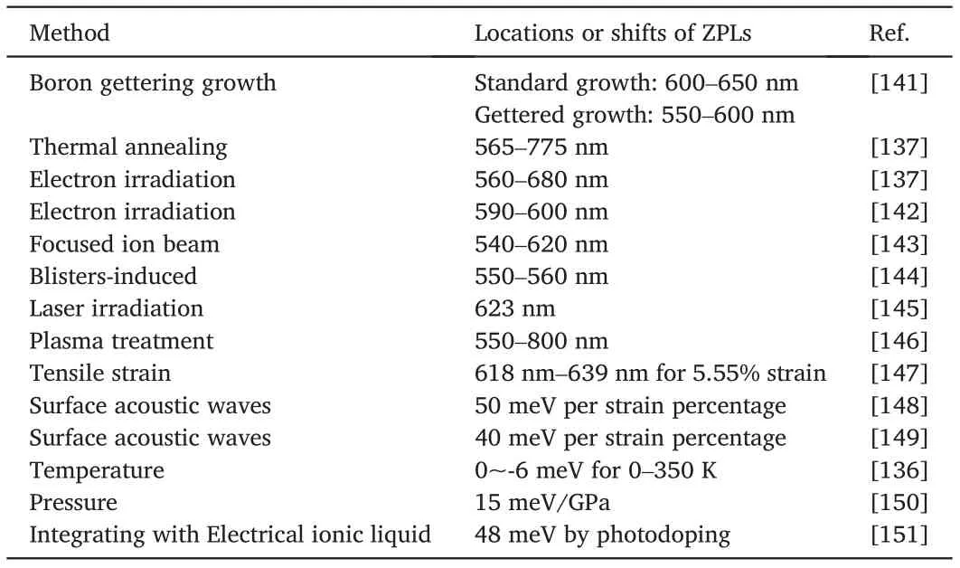
Table2 Summary of strategies to generate and tune SPEs in hBN.
4.3.Applications of SPEs in hBN
Due to the limited degree of understandings of mature hBN synthesis methods and on-chip devices fabrication technologies,widespread utilization of SPEs in hBN in industry is still in early stage.However,plenty of efforts have been made to explore the possibility of realizing efficient applications of SPEs in hBN.
Single photons play a key role in quantum information technologies as it can serve as information carrier in quantum systems.Quantum random number generation(QRNG)was achieved by on-chip coupling of SPEs in hBN with photonic circuit[152].After excitation,single photons were generated at a rate of~1MHz,which were subsequently detected by four avalanche photodiodes(APDs)after narrowing ZPL distribution and polarization.Therefore,random binary numbers from“0000”to“1111”,which refers to0to15in standard number,are generated by detecting the time-tagged photon arrivals.Theoretically,the number of bits yielded by a single photon can be extended by adding more APDs.The generated data stream was tested to have good randomness and this designed QRNG platform is stable and promising for quantum information processing.
Quantum light emission could be remarkably enhanced by coupling hBN quantum emitters to photonic crystal cavities(PCCs)[153].PCCs play the role of altering local photonic density and narrowing the linewidth of the emissions.In this reported work,Si3N4was chosen as the cavity materials due to its similar refractive index to hBN and relatively mature fabrication protocol.The functionalities of the PCCs did not noticeably change with the introduction of hBN and maintained high quality factor(Q-factor)up to3300.Some emitters in hBN were found to be coupled to the mode resonance of PCCs,resulting the emission enhancement of up to9.Such hybrid system will be beneficial for the utilization of SPEs in hBN for quantum networks.
In addition to the application in quantum system,SPEs in hBN can also be utilized in nano-scale measurement and metrology.A hBN-based optical thermometry was developed for local temperature measurement[154].The ZPL and linewidth of the emission are quite sensitive to temperature,which is the working principle of the thermometer.Meanwhile,the high brightness of the emitters in hBN offers satisfied performance in single emitters so that the spatial resolution of the thermometer is higher than that of conventional ensemble emitters.The fabricated thermometer showed better sensitivities over a large temperature range from0to800K,which attributes to the stability of the SPEs in hBN.
5.Summary and outlook
Abundant research has been conducted on the controllable synthesis of high-quality hBN crystals and thin films with desirable properties.Compared to other synthesis methods,CVD is the most promising route to grow hBN with a high yield and satisfactory tunability.In this review,we systematically summarized the recent progress from CVD growth mechanisms to controlled synthesis of hBN.To obtain large size of hBN crystals,common strategies focus on adjusting nucleation density,which can be reduced by modifying the substrate surface,configuration and composition.The substrates surface has strong effects on the hBN epitaxial growth.By properly constructing the metal edges,it is feasible to obtain large scale single crystalline hBN film by seamless stitching of uniformly oriented hBN grains via edge-coupling-guided growth.The layer number of hBN can be controlled by adjusting the growth pressure,temperature and precursor concentration,etc.We also reviewed relevant pioneering works that encompass one of the significant applications of hBN,single photon emission,including the origins of SPEs and strategies to generate and selectively tune the SPEs in hBN such as plasma and thermal treatment,laser and electron beam irradiation,surface acoustic waves,etc.
Even though recent work has achieved wafer-scale single-crystalline hBN growth by inducing uniform orientated hBN epitaxial growth and seamless stitching,there are still challenges regarding integrating largescale industrial applications of hBN with the quantum system.Uniform hBN crystals or thin films with precise layer number control have not yet been attained.Fostering synthesis methods that allow more precise control,such as uniform bilayer or multilayer hBN,are still at the incipient stage of development.Meanwhile,the effects of different strategies to tune hBN characteristics on its SPE generations also require further investigations.Edges of hBN crystals offer more emission sites[143],and it allows us to control the SPEs by tuning the growth morphology of hBN grains.Experimental and theoretical results indicate that monolayer and bilayer hBN will have pressure-dependent SPEs responses like ZPLs shift direction[150].For the influence of other properties,such as domain size,growth orientations and stacking orders,SPEs can serve as a powerful tool to investigate the corresponding defect formations in hBN,thus offering more precise controlling of SPEs formations.
Elucidating the detailed mechanism and providing direct experimental evidence to the origins of SPEs has also been particularly challenging.Recently,it was speculated that visible SPEs originate from carbon-related defects based on their experimental observations,offering the first experimental results to investigate the origins of SPEs[155].Nonetheless,many more efforts on the direct demonstration of the origin and precise tuning of SPEs are still greatly needed.Even though2D hBN is regarded as the most promising candidate as single photon emitters,there is still a long distance to the scale-up its applications with numerous obstacles.For example,despite the successful growth of wafer-scale single crystalline hBN[79,80],the uniformity and quality of the defect sites are still pending issues.In addition,successful integration of hBN on chips with satisfied emission brightness has not been reported while it would be undoubtedly a great step for further utilization of hBN-based emitters.Therefore,there still lies plenty of opportunities and challenges for further developing the synthesis of2D hBN and acquiring an in-depth understanding of its properties.
Declaration of competing interest
The authors declare no conflict of interest.
Acknowledgement
Z.L.acknowledge the support from Research Grant Council of Hong Kong SAR(16304518),NSFC-RGC Joint Research Scheme(N_HKUST607/17),the Innovation and Technology Commission(ITCCNERC14SC01)and the Zhongshan City Burea of Science and Technology(2019AG018)and the IER foundation(HT-JD-CXY-201907),research fund of Guangdong-Hong Kong-Macao Intelligent Micro-Nano Optoelectronic Technology Joint Laboratory(NO.2020B1212030010)and Guangdong Provincial Department of Science and Technology(grants2020A0505090003).
杂志排行
Namo Materials Science的其它文章
- Low-cost fabrication of highly dispersed atomically-thin MoS2nanosheets with abundant active Mo-terminated edges
- Hierarchically electrospun nanofibers and their applications:A review
- RTV silicone rubber composites reinforced with carbon nanotubes,titanium-di-oxide and their hybrid:Mechanical and piezoelectric actuation performance
- Advanced carbon materials with different spatial dimensions for supercapacitors
- Surface microstructure-controlled ZrO2for highly sensitive room-temperature NO2sensors
- Applications of carbon nanomaterials in perovskite solar cells for solar energy conversion
