I mpact of switching frequencies on the TID response of SiC power MOSFETs
2021-08-26ShengYangXiaowenLiangJiangweiCuiQiwenZhengJingSunMohanLiuDangZhangHaonanFengXuefengYuChuanfengXiangYudongLiandQiGuo
Sheng Yang, Xiaowen Liang, Jiangwei Cui Qiwen Zheng Jing Sun Mohan LiuDang Zhang Haonan Feng, Xuefeng Yu, Chuanfeng Xiang Yudong Li and Qi Guo
1Key Laboratory of Functional Materials and Devices for Special Environments, Xinjiang Technical Institute of Physics and Chemistry,Chinese Academy of Sciences, Urumqi 830011, China
2Xinjiang Key Laboratory of Electronic Information Material and Device, Urumqi 830011, China
3University of Chinese Academy of Sciences, Beijing 100049, China
Abstract: Different switching frequencies are required when SiC metal–oxide–semiconductor field-effect transistors (MOSFETs)are switching in a space environment.In this study, the total ionizing dose (TID) responses of SiC power MOSFETs are investigated under different switching frequencies from 1 kHz to 10 MHz.A significant shift was observed in the threshold voltage as the frequency increased, which resulted in premature failure of the drain–source breakdown voltage and drain–source leakage current.The degradation is attributed to the high activation and low recovery rates of traps at high frequencies.The results of this study suggest that a targeted TID irradiation test evaluation method can be developed according to the actual switching frequency of SiC power MOSFETs.
Key words: SiC power MOSFET; switching frequency; oxide trap; total ionizing dose; transistor; semiconductor theory
1.Introduction
Silicon carbide (SiC) metal–oxide–semiconductor fieldeffect transistors (MOSFETs) have the advantages of high frequency, high efficiency, and high current density compared with Si devices.These advantages have attracted attention in the pursuit of lightweight structures, miniaturization,and low power consumption in the aerospace electronics industry; therefore, SiC power MOSFETs have very broad applications in the aerospace field[1,2].However, owing to the sensitivity of MOS devices to space radiation and the high requirements for the reliability of electronic devices in the space environment, it is necessary to fully test and evaluate the application of SiC power MOSFETs in space electronic systems[3].
In the space radiation environment, the total ionizing dose (TID) induced by gamma rays is one of the most important factors that cause the failure of electronic devices.Recently, the radiation response of SiC power MOSFETs to gamma ray irradiation has been studied by several authors[4–8]since SiC high-voltage power MOSFETs have become commercially available.Thus far, the radiation response has been studied in terms of irradiation conditions,such as the temperature[4–6]and application of gate bias[7–9].It has been shown that the radiation-induced holes move toward the SiC/SiO2interface owing to the applied electric field, and they are trapped by defects in the oxide near the interface[10,11].However, in practical applications, SiC power MOSFETs are more often in the dynamic switching state at different frequencies.In the space environment, SiC power MOSFETs can be used in space solar inverters[12,13], electric thrusters, etc.[14]; the operating frequencies of these devices vary from kHz to MHz, as shown in Fig.1[15].Few studies have been conducted on the radiation effects under the dynamic frequencies of SiC power MOSFETs.Kobayashi[16]reported the gamma-ray irradiation response of the motor-driver circuit with SiC MOSFETs, but this was based on a specific frequency.The influence of a variation in the switching frequency on the radiation damage characteristics of devices has not been fully explored.Therefore, it is of great significance to study the influence and mechanism of the switching frequency of SiC power devices on the radiation damage characteristics.
In this study, the relationship of the performance of SiC power MOSFETs and switching frequencies varying from 1 kHz to 10 MHz is first explored in the harsh TID environment.On the basis of the above work, the mechanism by which the operating frequency influences the radiation response characteristics of the device is further discussed, and we propose that it is feasible to improve the radiation resistance ability of SiC power MOSFETs by appropriately changing the switching conditions.
2.Experimental details
The experimental devices used were commercial 44 A 1200 V N channel SiC MOSFETs (CGE1M120060) fabricated at the Beijing Cengol Semiconductor Co., Ltd..on 4H-SiC epitaxial layers.In fact, our experimental devices include SiC MOSFETs of Cree (C2M0080120D) and Rohm(SCT2450KE).Since the experimental results are basically similar, we only presentthe experimental results of this device (CGE1M120060) below.The samples were divided into five groups.The gate signal amplitude was 15 V, the high potential was 15 V, the low potential was 0 V, and the duty cycle was 50%.The switching frequencies of the five groups were set at 1 kHz, 10 kHz,100 kHz, 1 MHz, and 10 MHz.The control group was divided into two groups: the first group was biased at 0 V gate bias,and the second group was exposed at a positive voltage of 15 V.

Fig.1.Potential application examples using SiC devices at various voltage and frequency levels[15].
In the experiment, according to the test conditions given in the device manual, BC3193 was used to measure the breakdown voltage BVDSSand drain–source leakage currentIDSSof the devices at room temperature (25 °C).A Keithley 4200CSC semiconductor device analyser was used to test the threshold voltageVthbefore and after irradiation.These samples were irradiated at the Xinjiang Institute of Physics and Chemistry, Chinese Academy of Sciences by using a60Co-γsource up to 300 krad(Si) at a dose rate of 200 rad (Si)/s.
3.Results and discussion
Fig.2 shows the changes in the threshold voltageVthin the total dose radiation environment of SiC power MOSFETs under the operating states of ON, OFF, and different frequencies.As shown in Fig.2(a), The degradation inVthwas minimized at the off operating state with a gate bias of 0 V, while it was maximized when the gate bias was 15 V.The degradation varied at different frequencies between these two offsets.Note that the drift ofVthincreased with the increase in the operating frequency at the same dose point (see the discussion and analysis below and Fig.2(b)).
Fig.3 shows the relationship between the drain–source leakage currentIDSS(Fig.3(a)) and the drain–source breakdown voltage BVDSS(Fig.3(b)) of the SiC power MOSFET with various total doses under the ON, OFF, and switching conditions of different frequencies.As shown in Fig.3, the trend of the two parameters with the change in the dose point of the irradiation was not the same exactly; the drain–source leakage currentIDSSwith the total ionizing dose gradually increases and the breakdown voltage significantly decreases when the total ionizing dose reaches a certain value.However, they all showed that the damage degradation strongly depended on switching frequency.For example, as shown in Fig.3(b), under the same circumstances, SiC power MOSFETs switching on 10 MHz irradiation to 150 krad (Si) completely lost their blocking function, and 1 kHz samples in the 250 krad(Si) region lost the ability to block high voltage.
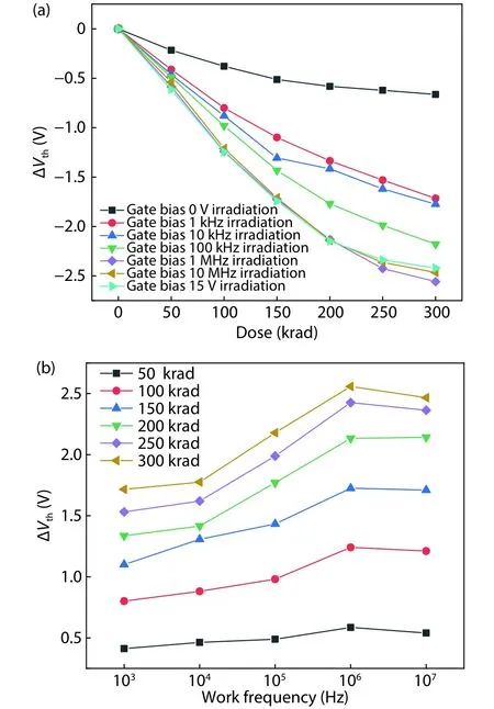
Fig.2.(Color online) SiC power MOSFET.(a) Variation in threshold voltage with the total ionizing dose at ON, OFF, and different frequencies.(b) Relation between the change in threshold voltage and applied switching frequency under the same total ionizing dose.
The degradation of the properties and parameters of SiC power MOSFETs in the total dose radiation environment is mainly attributed to the oxide charge and interface states generated and accumulated by ionizing radiation near the SiC/SiO2interface[10].The amount of oxide charge and interfacial state are directly related to the bias state of the gate oxide layer[17]: a large number of electron–hole pairs are created in the oxide by the ionizing radiation, and under the zero-bias condition, the pairs quickly recombine.Therefore,the probability of the hole being captured by the interface trap to form a trap charge is not high.However, under a positive gate bias, because the electron mobility is considerably higher than the hole mobility in SiO2, most electrons will quickly drift to the gate, and the hole will drift to the SiC/SiO2interface, which greatly increases the probability of the interface trap capturing these holes.Thus, in general, the radiation damage of the MOS transistors is minimized at a gate bias of 0 V, while the damage is maximized under the condition of a positive bias.
Under a switching frequency bias, although the bias voltage changes constantly, its range is between 0 and 15 V.Therefore, this mechanism also explains the parameters and performance degradation of SiC power MOSFETs at different frequencies.If we continue to infer according to this model, it is reasonable to conclude that the radiation degradation should be approximately the same regardless of the operating frequency, because under the 50% duty cycle condition,the total time of the 0 V bias and the total time of the 15 V bi-as during irradiation do not vary with frequency.Our test results show that the radiation damage, including the parameters and function of the SiC power MOSFETs, depends on the operating frequency to a certain extent.The static ionising radiation damage model of the SiC power MOSFETs cannot explain the actual radiation damage in the dynamic switching state.
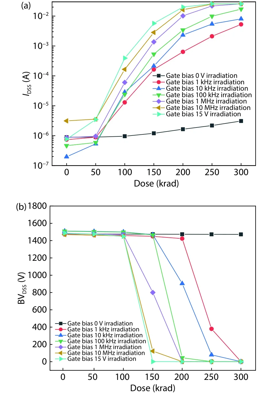
Fig.3.(Color online)SiC power MOSFETs at ON, OFF, and different frequencies.(a) Variation in drain–source leakage current with the total ionizing dose.(b) Change in breakdown voltage with the total ionizing dose.
We can try to understand the above phenomenon with the oxide hole trap model of the US Army Research Laboratory (ARL)[18].As shown in Fig.4, there is a weak Si–Si bond at the SiC/SiO2interface; therefore, there is an oxygen vacancy near the interface.Once these weak bonds are broken (owing to the ionizing radiation), an active trap, known as the E centre, is formed.It can either capture holes that are positively charged, or it can be thermally excited, ionized, or tunnelled through electron recombination, making it electrically neutral.This process is usually repeatable[19,20].For the switching frequency bias in this experiment, when the signal had a high potential, under the action of a positive gate electric field, a large number of net holes were present at the SiC/SiO2interface, and it was easy for the E centre generated by the irradiation to capture these net holes and form a trap charge.This led to a drift or the degradation of the threshold voltage and other parameters.When the signal was at a low potential (0 V), some of the captured holes gradually broke away from the trap and recombined with the ionised electrons and tunnelling electrons, resulting in the recovery of the threshold voltage to some extent.However, owing to the low mobility of the hole and the absence of a driving electric field, the recovery of damage was rather slow.The degree of recovery strongly depended on the signal frequency.At relatively low frequencies, there was a sufficient time for damage recovery at low levels; therefore, the overall radiation damage was small, and as the frequency increased, the duration of the low level became shorter, so that the probability of the hole escaping from the trap and electron recombination became lower.Thus, with an increase in the frequency, the radiation damage of the device was aggravated.
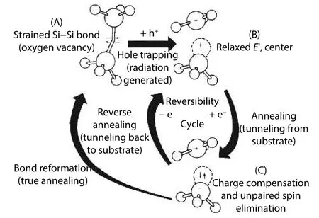
Fig.4.A model hole trapping [(a) to (b)]and detrapping [(c) to (a)]processes are indicated, along with the intermediate compensation/reverse-annealing phenomenon [(b) to (c) and (c) to (b)][18].

Fig.5.(Color online) Comparison of threshold voltage of SiC Power MOSFETs with the total ionizing dose under 15 and 0 V segment gate bias, constant 0 V gate bias, and constant 15 V gate bias.
To further verify our inference, we designed another irradiation experiment with an alternating gate bias at 15 and 0 V with different total doses under the same experimental conditions; the experimental results are shown in Fig.5.No obvious recovery of the threshold voltage was found at the first low potential, because the positive charge accumulation process was stronger than the recovery process.At the second and third low potentials, a significant recovery of the threshold voltage was observed.At the dose point of 300 krad (Si), the negative drift of the threshold voltage was approximately –1.5 V, and this value is lower than the degradation seen in Fig.2 under the minimum value of 1 kHz.These experimental results have confirmed the accuracy of our theoretical analysis to a certain extent.
4.Conclusion
In summary, the results of this study show that TID radiation damage of the SiC power MOSFETs is related to the magnitude and direction of the electric field applied during irradiation, and it also strongly depends on the operating frequency.Under the same conditions, the TID radiation damage of SiC power MOSFETs will be aggravated as the frequency of the device increases.Further, a low frequency can be consciously selected or reduced to improve the radiation resistance ability of SiC power MOSFETs under permissible application conditions.The results suggest that we can develop a targeted TID test evaluation method according to the actual switching frequency of SiC power MOSFETs.
Acknowledgements
This work was supported by the National Natural Science Foundation of China under Grant No.11975305 and the West Light Foundation of The Chinese Academy of Sciences,Grant No.2017-XBQNXZ-B-008.
杂志排行
Journal of Semiconductors的其它文章
- Reliability evaluation on sense-switch p-channel flash
- Targeted transfer of self-assembled CdSe nanoplatelet film onto WS2 flakes to construct hybrid heterostructures
- First-principles study of the growth and diffusion of B and N atoms on the sapphire surface with h-BN as the buffer layer
- Low-cost dual-stage offset-cancelled sense amplifier with hybrid read reference generator for improved read performance of RRAM at advanced technology nodes
- Ultra-low Vpp and high-modulation-depth InP-based electro–optic microring modulator
- Extensive study of optical contrast between bulk and nanoscale transition metal dichalcogenide semiconductors