Reliability evaluation on sense-switch p-channel flash
2021-08-26SideSongGuozhuLiuHailiangZhangLichaoChaoJingheWeiWeiZhaoGenshenHongandQiHe
Side Song, Guozhu Liu,, Hailiang Zhang, Lichao Chao, Jinghe Wei, Wei Zhao,Genshen Hong, and Qi He
1The 58th Institution of Electronic Science and Technology Group Corporation of China, Wuxi 214035, China
2School of Electronic Science and Engineering, Southeast University, Nanjing 210096, China
Abstract: In this paper, the reliability of sense-switch p-channel flash is evaluated extensively.The endurance result indicates that the p-channel flash could be programmed and erased for more than 10 000 cycles; the room temperature read stress shows negligible influence on the p-channel flash cell; high temperature data retention at 150 °C is extrapolated to be about 5 years and 53 years corresponding to 30% and 40% degradation in the drive current, respectively.Moreover, the electrical parameters of the p-channel flash at different operation temperature are found to be less affected.All the results above indicate that the sense-switch p-channel flash is suitable to be used as the configuration cell in flash-based FPGA.
Key words: reliability; endurance; data retention; sense-switch p-channel flash
1.Introduction
With the rapid development of aerospace technology,the demand for highly qualified and highly reliable electrical and electronic systems is stronger and stronger.FPGA (field programmable gate array) is an important class of integrated circuit device used in aerospace electronics.There are mainly three kinds of FPGAs, the antifuse-based FPGA[1,2], the flashbased FPGA[3−6]and the SRAM-based FPGA[7,8].Among them,the antifuse-based FPGA is one-time programmable (OTP)and only a limited density could be reached.Although the SRAM-based FPGA could be as large as billion gates level, it is vulnerable to single event upset and it is volatile, while the flash-based FPGA is considered as the next mainstream technology for its high safety, high reliable, radiation hardened, nonvolatile and reprogrammable properties.
To the best of our knowledge, the configuration cells for flash-based FPGA mainly include sense-switch and pushpull[9,10].The sense-switch n-channel flash has already been applied to the Microsemi’s series product ranging from 0.25μm to 65 nm, but its reliability and radiation hardness are quite challenging.While there are few reports on sense-switch pchannel flash, compared with n-channel flash, p-channel flash has its special advantages in high-speed programming and low-power operation[11], as well as the intrinsic radiation hardness[12,13].Thus, it is meaningful and valuable to have an overall evaluation on the sense-switch p-channel flash, aiming to make high reliable flash-based FPGA.
In this letter, the reliability of sense-switch p-channel flash was evaluated with emphasis on endurance and data retention.It is assured that the sense-switch p-channel flash could be programmed and erased for more than 10 000 cycles with only 1.3 V threshold voltage window closing and 30% drive current degradation.The data retention ability at 150 °C is extrapolated to be 5 years (when a criteria of 30% degradation in drive current is used); moreover, the electrical parameters of the p-channel flash at different temperature are monitored.All the results indicate that the sense-switch p-channel flash has the potential to be applied into flashbased FPGA.
2.Experiment
The sense-switch p-channel flash was manufactured using 130 nm embedded flash technology.Fig.1(a) depicts the cell structure.A sense-switch device consists of two transistors, the sense transistor, which is used for program, erase and verify operations, and the switch, which is randomly wired to logic devices for signal propagation.It is noted that both the sense (T1) and switch (T2) transistor share the same control gate and floating gate, when T1 is programmed, the floating gate will be filled with electron and the channel of T2 is turned on.When T1 is erased, the electron is ejected from the common floating gate and T2 is turned off, as shown in Fig.1(b).
The reliability evaluation is mainly focused on endurance and data retention.For endurance evaluation, the devices are programmed and erased for as long as 10 000 cycles, the electric characteristics were monitored.The data retention ability is tested at both the room temperature and high temperature for a typical stress duration.Last but not least, theI–Vcharacteristics of the sense-switch p-channel flash at different temperature are measured.For each evaluation, at least five devices are chosen to increase the accuracy.It should be noted that all the device characteristics monitored in the following were limited only to the switch transistor (T2).
3.Results and discussion
3.1.Endurance
The threshold voltage (Vth, collected by constant currentatId= –0.1μA) and drive current (Ion=Id@Vd= –1.5 V,Vcg=0 V) as a function of program and erase cycles is shown in Fig.2(a).Both theVthafter programming and erasing shift toward the negative direction, where the programmedVthsees a larger shift (2.5 V) than the erasedVth(1.2 V), resulting in aVthwindow closing from 11.1 V at initial to 9.7 V from the initial to 10 000 program and erase cycles.The drive current exhibits a first slow and then fast drop-down phenomenon, and the drive current decreases about 30% up to 10 000 cycles.
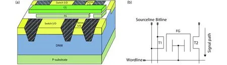
Fig.1.(Color online) (a) The three-dimensional sense-switch p-channel flash diagram.(b) The basic working schematic.
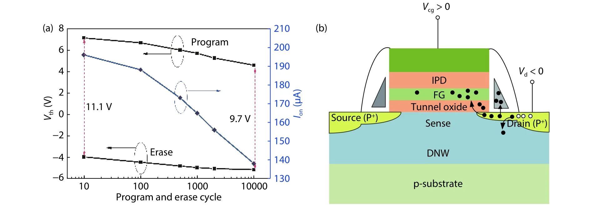
Fig.2.(Color online) (a) The threshold voltage and drive current as a function of the program and erase cycles.(b) Electron trapping in the tunnel oxide or spacer at the drain side when programmed.
The reasons forVthshift and drive current degradation are in close link with the tunnel oxide and spacer at the drain side[14,15].As in our case, the sense-switch p-channel flash cell is programmed by BBHE (band-to-band tunneling induced hot electron), which is a high-speed and low-power programming method for p-channel flash, but it may cause damage to the tunnel oxide more severely than CHHIHE (channel hot hole-induced hot electron)[16].The BBHE program mechanism features a positive voltage on the control gate and a negative bias on the drain and, under such a bias condition, electron–hole pairs are generated at the gate/drain overlap region due to energy band bending.The electron is accelerated because of large lateral potential gradient created by drain-to-substrate voltage, some of these electrons may inject into the floating gate in favor of the vertical electric field,while some are trapped into the tunnel oxide or the spacer due to defects generated by the manufacture process or repeated electron tunneling process[15].At the first hundred cycles, the oxide or space trap density is low and the programmedVthis less affected, with increasing the cycles, more and more traps are generated, as illustrated in Fig.2(b),which will significantly degrade the program speed, thus the programmedVthdrops faster.The relationship ofVthshift(ΔVth) to the trapped electron in the tunnel oxide is described as
where ΔQis the density of trapped electrons in the tunnel oxide,εis the dielectric constant of the tunnel oxide anddis the thickness of the tunnel oxide.Lower programmedVthmeans less electron on the common floating gate, which in turn increases the channel resistance of the switch transistor,leading to an obvious drop-down of the drive current.
After all, the sense-switch p-channel flash is endurable to more than 10 000 program and erase cycles, in comparison to the sense-switch n-channel flash (more than 1000 program and erase cycles[15]).Therefore, the sense-switch p-channel flash is endurable to be applied to Flash-based FPGA.
3.2.Data retention
The evaluation on sense-switch p-channel flash’s data retention ability is carried out both in room temperature and high temperature.Fig.3(a) is the current-time curve measured with drain bias at –1.5 V, control gate bias at 0 V, grounded source and substrate for the programmed state switch transistor at room temperature.Fig.3(b) depicts theI–Vcharacteristic of the sense-switch p-channel flash before and after 100 000 s read stress.Both curves show that the p-channelflash is unaffected by room temperature read stress.
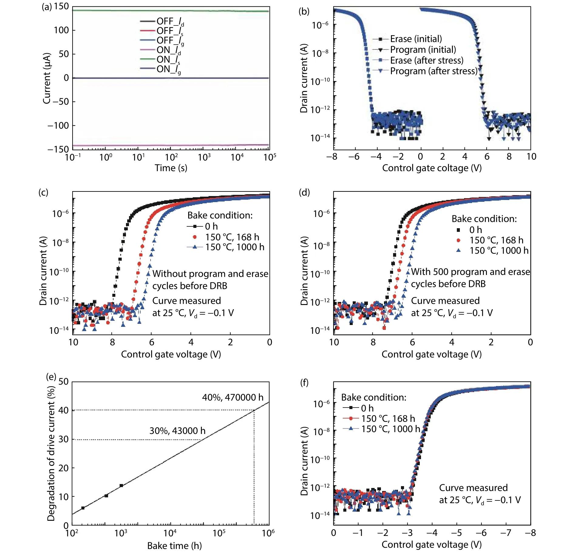
Fig.3.(Color online) (a) Current–time curve during read stress at room temperature.(b) I–V characteristic before and after read stress.I–V characteristic before and after high temperature storage (c) without cycling and (d) with 500 program and erase cycles before DRB.(e) Degradation of drive current versus time in bake.(f) I–V characteristic of the erased state device under high temperature storage.
The high temperature data retention experiment is carried out both for the programmed and erased flash devices,with a typical bake temperature (150 °C) and time (1000 h),the results are shown in Figs.3(c)–3(f).Figs.3(c) and 3(d) represent the p-channel flash without and with 500 program and erase cycles before the bake process, respectively.For those without being cycled before baking, theVthshift is about 1 V, in comparison to 0.4 V for the device with 500 program and erase cycles, in the first 150 °C, 168 h bake duration.While in the next 168–1000 h duration, both devices exhibit a similarVthshift of about 0.5 V.Two possible reasons are proposed to explain the difference: Firstly, those devices without cycling first before baking have a more positive threshold voltage (~6.8 V), corresponding to larger amount of electrons on the floating gate and lower intrinsic potential,when they are subjected to high temperature bake, more electron can gain energy and escape either through the tunnel oxide[17]or the interpoly dielectric[18].Secondly, the trapped electron in the tunnel oxide induced by repeated program and erase may inhibit extra electron loss from the floating gate.
Fig.3(e) reports the degradation of drive current (collected atVd= –1.5 V andVcg=Vb=Vs= 0 V) as function of the high temperature bake time, the data fit a log-linear relationship that can be extrapolated to 30% degradation at 43 000 h (about 5 years) and 40% degradation at 470 000 h(about 53 years), at 150 °C, in comparison to Microsemi’s RT ProASIC3 devices’ data retention (less than 10 years at 150 °C).Moreover, the erased state p-channel flash under high temperature bake was also investigated, as shown in Fig.3(f), and no obvious change was found in the 150 °C,1000 h time duration.The results above indicate that the sense-switch p-channel flash has good data retention properties under high temperature ambient.
3.3.Temperature related performance
The electrical parameters of the sense-switch p-channel flash under different temperature conditions are also tested,as reported in Fig.4.The drive current of programmed stateatVd= –1.5 V andVcg= 0 V (see Fig.4(a)) increases about 10% (at –55 °C) and drops about 14% (at 125 °C) in comparison with the value measured at room temperature (25 °C).TheVthshift (see Fig.4(b)) is less than 1 V in the –55 to 125 °C temperature range.Specifically, a thermal cycling experiment between 25 and 125 °C is carried out and the result is reported in Fig.4(c).Except for the first two cycles, where theVthand drive current drops a little, the next cycles are quite stable and reproducible.The results above show that the sense-switch p-channel flash is robust in low and high temperature, even with a sudden change of the temperature, once again lays a foundation for the investigation of sense-switch p-channel flash used as configuration cells for flash-based FPGA.
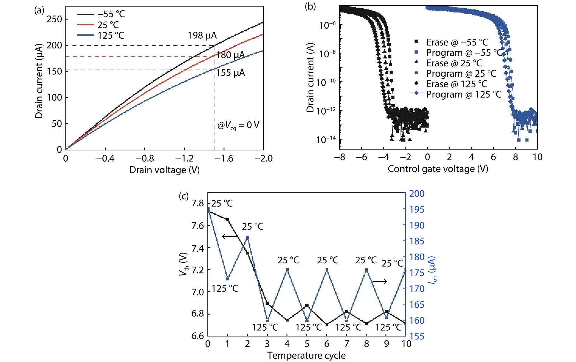
Fig.4.(Color online) (a) The output characteristics of the programmed switch.(b) The programmed and erased state of the switch under different temperatures.(c) The threshold voltage and drive current with different temperature cycling.
4.Conclusion
The reliability of sense-switch p-channel flash concerning endurance and data retention were evaluated on emphasis.The endurance experiment suggests that the sense-switch p-channel flash could be programmed and erased for more than 10 000 cycles with only 1.3 V threshold voltage window closing and 30% drive current degradation, which is mainly due to the electron trapping in the tunnel oxide or spacer at the drain side.The room temperature read stress has a negligible effect on the p-channel flash, and the data retention ability at 150 °C is extrapolated to be 5 years (when a criteria of 30% degradation in drive current is used) and about 53 years(when a criteria of 40% degradation in drive current is used).Furthermore, the p-channel flash is proved to be robust and endurable at different temperatures or suffer from a sudden temperature change.All the results indicate that the senseswitch p-channel flash is a potential configuration cell for flash-based FPGA.
杂志排行
Journal of Semiconductors的其它文章
- I mpact of switching frequencies on the TID response of SiC power MOSFETs
- Targeted transfer of self-assembled CdSe nanoplatelet film onto WS2 flakes to construct hybrid heterostructures
- First-principles study of the growth and diffusion of B and N atoms on the sapphire surface with h-BN as the buffer layer
- Low-cost dual-stage offset-cancelled sense amplifier with hybrid read reference generator for improved read performance of RRAM at advanced technology nodes
- Ultra-low Vpp and high-modulation-depth InP-based electro–optic microring modulator
- Extensive study of optical contrast between bulk and nanoscale transition metal dichalcogenide semiconductors