Ultra-low Vpp and high-modulation-depth InP-based electro–optic microring modulator
2021-08-26DapengLiuJianTangYaoMengWeiLiNinghuaZhuandMingLi
Dapeng Liu, Jian Tang, Yao Meng, Wei Li, Ninghua Zhu, and Ming Li,
1State Key Laboratory of Integrated Optoelectronics, Institute of Semiconductors, Chinese Academy of Sciences, Beijing 100083, China
2School of Electronic, Electrical and Communication Engineering, University of Chinese Academy of Science, Beijing 100049, China
Abstract: A modulator is an essential building block in the integrated photonics, connecting the electrical with optical signals.The microring modulator gains much attention because of the small footprint, low drive voltage and high extinction ratio.An ultra-low Vpp and high-modulation-depth indium phosphide-based racetrack microring modulator is demonstrated in this paper.The proposed device mainly comprises one racetrack microring, incorporating a semiconductor amplifier, and coupling with a bus waveguide through a multimode interference coupler.Traveling wave electrodes are employed to supply bidirectional bias ports, terminating with a 50-Ω impedance.The on/off extinction ratio of the microring reaches 43.3 dB due to the delicately tuning of the gain.An 11 mV Vpp, a maximum 42.5 dB modulation depth and a 6.6 GHz bandwidth are realized, respectively.This proposed microring modulator could enrich the functionalities and designability of the fundamental integrated devices.
Key words: integrated photonics; high-modulation-depth; microring modulator
1.Introduction
Integrated photonics is a hopeful way to solve the bottleneck of energy and speed, which mainly focuses on devices like laser, modulator, photodetector at the present stage[1−14].Microring modulator performing as the basic building block in the photonic integrated circuit (PIC), has received considerable attention in recent years.Features include small footprint, low drive voltage and high extinction ratio, which enable the application possibilities of microring modulators in on-chip optical interconnections.There are colorful studies about microring modulators reported, focusing on high speed, small scale, low voltage, low-power consumption,high order modulation, hybrid integration and novel structures[5,15−27].These devices are mainly fabricated on platforms like the silicon on insulator, lithium niobate and polymer[15,19−22,28−35].The basic characteristics of the microring resonator largely decide the performance of the microring modulator, which is hard to change once fabricated on these platforms.However, the attributes like quality factor and coupling coefficient of the microring resonator could be controlled by adjusting the gain in the microring resonance cavity[36,37].Based on the tuning of gain, an ultra-lowVppand high-modulation-depth microring modulator is implemented on an indium phosphide (InP)-based platform, enabling more tunability, designability and flexibility in PIC[38−41].And compared with the reported InP microdisk modulator, circular microresonators modulation, and slot waveguide microring modulator simulation, the proposed microring modulator shows lowerVppand higher modulation depth[12−14].
Here, we designed a microring modulator, in which the microring resonator incorporates a 500μm long semiconductor optical amplifier (SOA) and couples to the bus waveguide through a multimode interference (MMI) coupler.The SOA is implemented in the device to supply the gain and compensate for the propagation loss in the ring, which can adjust the transmission spectra of the resonator to achieve high-modulation depth.And the quantum-confined Stark effect (QCSE) in the microring modulates the refractive index to realize the modulation.Traveling wave electrodes are designed to inject the electrical signal to the SOA to realize the modulation.The free spectral range (FSR) of the device is 19.5 GHz around the resonance wavelength.The extinction ratio (ER) of the resonator is 43.3 dB and the resonance wavelength is 1550.002 nm.TheVppis as low as 11 mV and the modulation depth rises to a maximum of 42.5 dB.A 137.5 mA bias current is set to the SOA and a 6.6 GHz bandwidth is achieved.Eye diagrams are measured in which pseudo random binary sequence (PRBS) 27– 1 non-return-tozero (NRZ) data signals with speed up to 12 Gb/s are applied to the proposed device.The unique designed microring modulator shows a way of realizing the ultra-lowVppand high modulation depth.And the performance could be improved with further research.
2.Design and fabrication
Fig.1 shows the schematic diagram of the proposed microring modulator.The device is fabricated on the InP platform and mainly consists of a racetrack microring, which includes an SOA and is coupled to a bus waveguide through a MMI coupler.The incorporated SOA is 500μm long and designed to supply 10 dB gain at most.Maximum 20 GHz traveling wave electrodes are employed to SOA to realize the modu-belation,which are from the standard process design kite (PDK,supplied by HHI, Gemany). To achieve the maximum modulation speed, bias ports of the electrodes could be used bidirectionally,in which one of them should be terminated with a 50 Ω impedance. A 2 × 2 MMI coupler is used to connect the racetrack microring and the bus waveguide due to the good fabrication tolerance of the MMI coupler. Two spot size converters (SSCs) are adopted at the two ports of the bus waveguide,respectively. Distance between the two SSCs is
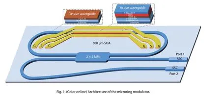
The bending radius of the racetrack microring is 300 μm and the perimeter is 4.14 , which indicates the free spectral range (FSR) is about 0.16 nm around 1550 nm wavelength. There are mainly two typical waveguides in this device: a passive waveguide and active waveguide. The differenceis that the passive waveguide suffers a lower loss (< 3 dB/cm) than the active waveguide. But the active waveguide could supply the gain because it includes the quantum wells (QWs) structure and realize stimulated emission amplification when the light is injected to the SOA. The critical coupling state can be achieved by delicately controlling the gain in the resonance cavity. Refractive index modulation induced by the QCSE in the QWs could modulate the transmission spectra,enabling the device as an electro–optic modulator.
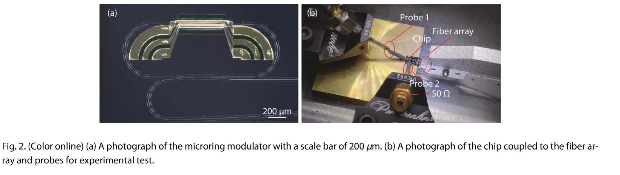
An optical microscope image of the device with a scale bar of 200 μm is shown in Fig. 2(a), in which the SSCs are outside the view because of the minimum magnification times lim itation.The way to couple the optical and electrical signal is illustrated in Fig. 2(b) that a two ports standard single-mode fiber array (FA) is coupled to the two ports of the microring modulator through SSCs. Probe 1 carries the electrical signal to one port of the traveling wave electrode on the chip, while probe 2 connects a 50 Ω impedance to the other port of the electrode. There is a copper block under the chip for heat dissipation.
3.Characterization and experimental results
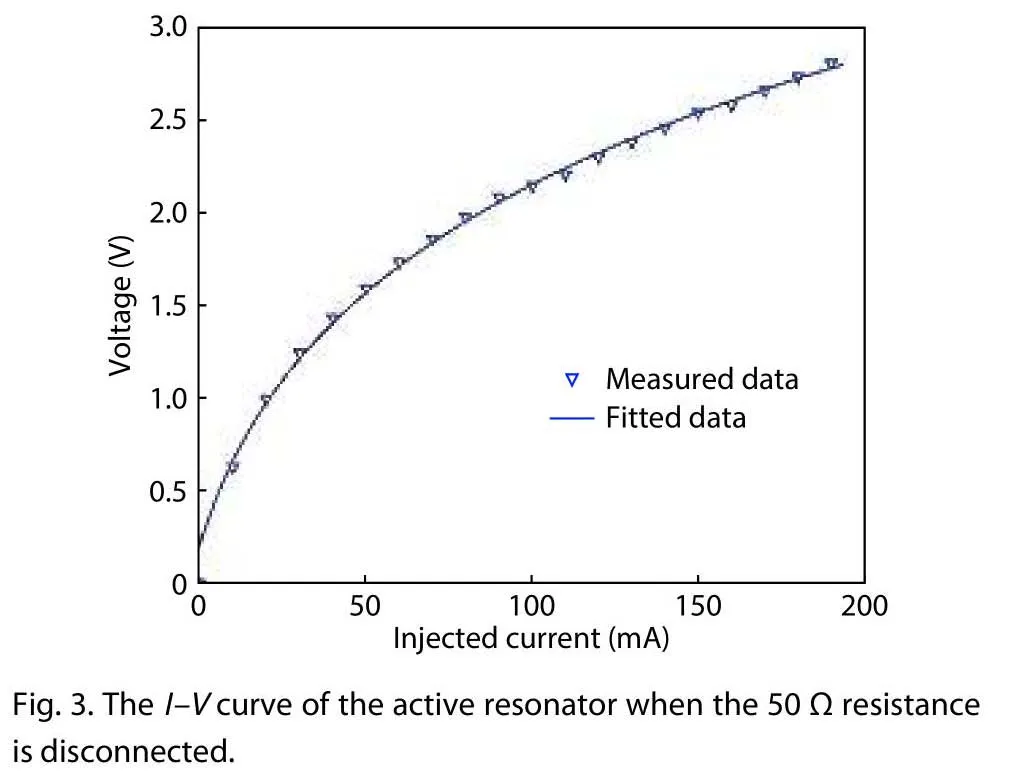
To characterize the modulator, theI–Vcurve of the SOA is measured when the 50 Ω impedance is disconnected be-cause the SOA is usually driven by injection currents.And theI–Vcurve could relate currents with the corresponding voltage.A source-measure unit (SMU) and a bias tee are applied to test theI–Vcurve which is plotted and fitted in Fig.3.Only a maximum 190 mA current is applied, avoiding the damage of the SOA.
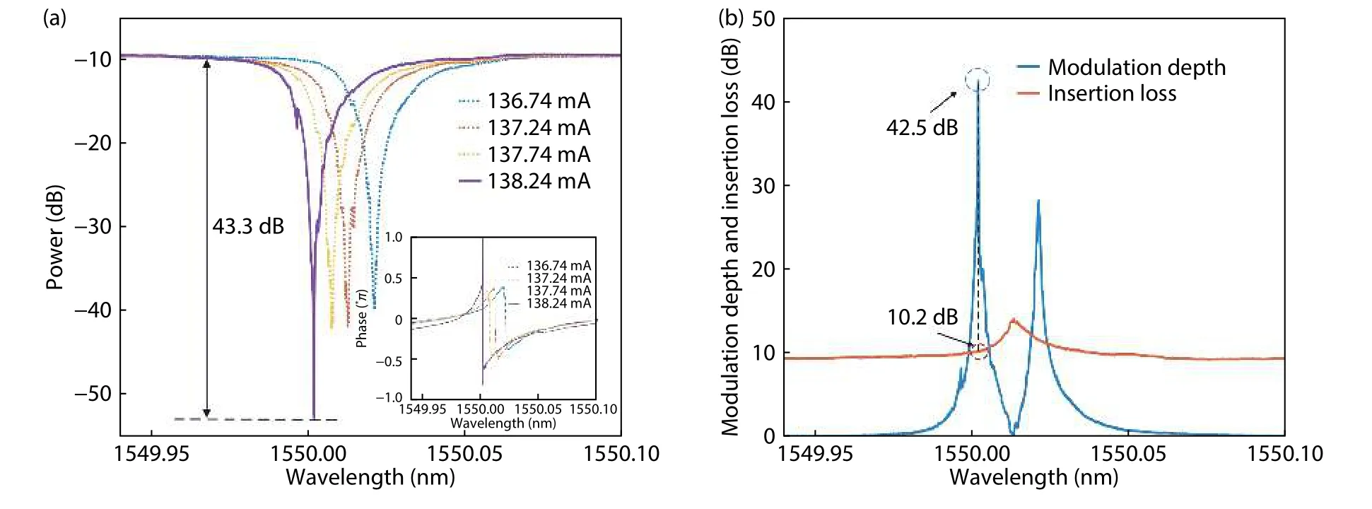
Fig.4.(Color online) (a) The transmission spectra of the microring modulator under four injection currents applied to the SOA.(b) Modulation depth and insertion loss with currents from 136.74 to 138.24 mA.
Then a high-resolution optical vector network analyzer(OVNA) is established to measure the static transmission and phase spectra of the designed microring modulator.An optical carrier generated by the laser (Yenista, Tunics T1005-HP)and modulated by radio frequency (RF) signal from the electrical vector network analyzer (ZVA 40) through the phase modulator (EOSPACE, 40G).And an optical double-sideband(ODSB) signal is produced and one sideband is filtered out by the tunable filter to generate an optical single-sideband(OSSB).The OSSB signal is amplified by an erbium-doped fiber amplifier (EDFA) and coupled to the chip via the input port SSC.After the transmission through the device, the OSSB signal is injected to one photodetector (FINISAR XPDV2120R)to beat and generate RF signal.The RF signal is fed back to the electrical vector network analyzer (EVNA) after the amplification of an electrical amplifier (EA).TheS21curve exhibits the transmission spectra of the device and the resolution is decided by the EVNA, which could achieve tens of Hz resolution.The characterization of the device could be more precisely measured by this OVNA[24,42].
The transmission spectra of the modulator at four different injection currents are displayed in Fig.4(a).There are four lines representing the transmission spectra of the device for 136.74, 137.24, 137.74, and 138.24 mA injection currents.When the current of SOA is set to 138.24 mA, the microring resonator operates around the ideal critical coupling point, in which the ER is over 43 dB.As improving the injection current, the gain of SOA could compensate for the loss in the microring.The current is delicately tuned to adjust the relation between the loss coefficient and coupling coefficient, while the transmission spectra could be observed in real time through OVNA.Once the coupling coefficient between the bus waveguide and the microring equals the loss coefficient in the microring, the active microring resonator will be under critical coupling condition, wherein the ER is theoretically infinite at the resonance wavelength.To estimate the coupling state of the microring resonator, the phase data recorded by the EVNA is processed with the formula:Phase(π)=(Degree/360)×2.And the degree is the recorded phase data.The phase-wavelength relation is shown in the insertion of Fig.4(a).It shows the phase transition at the resonance wavelength when the injection current is 138.24 mA, which is very close to the critical coupling state.Referring to the related work, the modulation depth and insertion loss could be easily calculated from Fig.4(a)[20].On/off modulation ratio and loss could be derived by spectral measurement with the injection currents to SOA (disconnects with the 50 Ω resistance) from 136.74 to 138.24 mA.As shown in Fig.4(b), there are two peaks of the modulation depth and the higher one is about 42.5 dB, in which the insertion loss is 10.2 dB.The insertion loss includes the two coupling points and the provided value from the PDK is less than 2 dB for per SSC.The proposed microring modulator could work at the two peaks.The insertion loss of the device should be lower than that in Fig.4(b) because of the butt-coupling loss.Moreover, according to theI–Vcurve in Fig.3, the applied injection currents:136.74, 137.24, 137.74, and 138.24 mA equal to the voltages:2.449, 2.453, 2.456, 2.460 V.According to the experiment results in Fig.3 and Fig.4, theVppis 11 mV (2.4449 to 2.460 V).Commonly, lowVppcontributes to lower power consumption,which means significant to the modulator and system.
To measure the modulation bandwidth, a 50 Ω impedance is applied to the chip to reduce the reflection of the microwave signal.The experiment link is shown in Fig.5.A 1550.005 nm carrier wave is coupled to the modulator to enable the microring modulator operate at the linear operating point.And a 186.6 mA bias current is applied, in which a 137.5 mA will be set to SOA according to theI–Vcurve in Fig.3(a) and the tested static transmission spectra in Fig.4(a).Using the EVNA to measure theS21of this modulator from 0 to 20 GHz with the power of 9 dBm, which is presented in Fig.6.The 3 dB bandwidth of the microring modulator is about 6.6 GHz.Because the traveling electrodes are from the standard PDK, the bandwidth is mainly limited by the QCSE.What is more, optimizing the electrode and waveguide design, improving the growth of InP quantum wells, and reducing the radius of the microring could improve the 3 dB bandwidth of the microring modulator.
Applied in the back-to-back configuration, eye diagrams are measured.Figs.7(a)–7(c) show measured eye diagrams un-der the transmission of 4, 8, and 12 Gb/s PRBS 27–1 NRZ data signals, respectively.As can be seen in Fig.7, the eye could open clear when the modulating signal reaches 8 Gb/s.Nevertheless, when the data speed exceeds 10 Gb/s, the eye diagrams are hard to open because of the noise and the nonlinearity in the test link.The proposed microring modulator may be employed in the optical communication link.To improve the modulation speed, the fabrication process and electrodes design could be modified.

Fig.5.(Color online) The experiment schematic of the modulation bandwidth measurement.
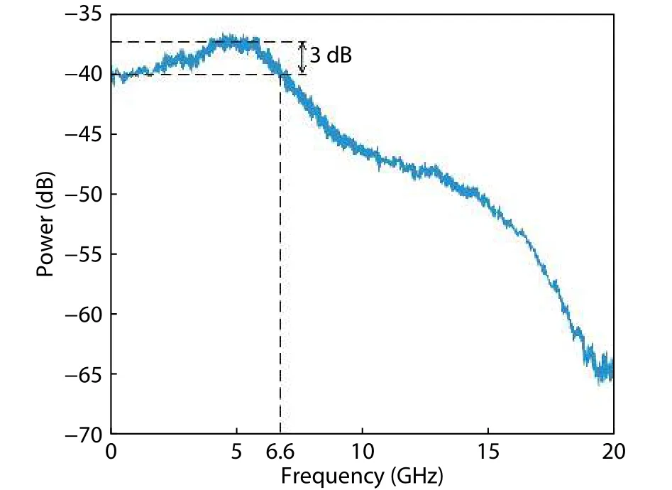
Fig.6.The bandwidth of the device when it works as an electro–optic modulator.
4.Conclusion
In conclusion, an ultra-lowVppand high-modulationdepth InP-based electro–optic microring modulator is designed, fabricated, and characterized.TheVppreaches as low as 11 mV and the modulation depth is 42.5 dB in maximum.The microring modulator shows a 6.6 GHz bandwidth and measured eye diagrams up to 12 Gb/s bit rate demonstrate the ability of the proposed device in the optical communication link.The realization of the microring modulator broadens the applications and promotes the designability of the basic building blocks in PIC.
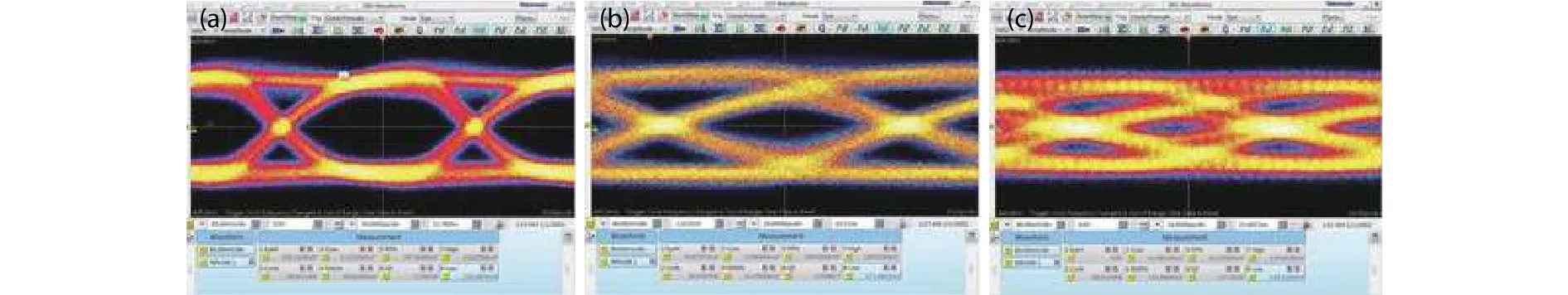
Fig.7.(Color online) Measured eye diagrams of the device under 4, 8, and 12 Gb/s bit rates.
Acknowledgements
This work was supported by the National Natural Science Foundation of China (61535012, 61925505) and the National Key R&D Program of China (2018YFB2201900).The authors acknowledge VLC, Spain, for their help in designing this chip.The authors acknowledge HHI, Germany, for the chip fabrication.
杂志排行

Journal of Semiconductors的其它文章
- Reliability evaluation on sense-switch p-channel flash
- I mpact of switching frequencies on the TID response of SiC power MOSFETs
- Targeted transfer of self-assembled CdSe nanoplatelet film onto WS2 flakes to construct hybrid heterostructures
- First-principles study of the growth and diffusion of B and N atoms on the sapphire surface with h-BN as the buffer layer
- Low-cost dual-stage offset-cancelled sense amplifier with hybrid read reference generator for improved read performance of RRAM at advanced technology nodes
- Extensive study of optical contrast between bulk and nanoscale transition metal dichalcogenide semiconductors