Extensive study of optical contrast between bulk and nanoscale transition metal dichalcogenide semiconductors
2021-08-26AnkushParmarJashangeetKaurManishDevSharmaandNavdeepGoyal
Ankush Parmar, Jashangeet Kaur, Manish Dev Sharma, and Navdeep Goyal
1Centre of Applied Sciences, Department of Physics, Sector-14, Panjab University, Chandigarh 160014, India
2Department of Physics, G.G.D.S.D College, Sector-32, Chandigarh 160030, India
Abstract: A remarkable refinement in the optical behavior of two-dimensional transition metal dichalcogenides (TMDs) has been brought to light when cleaved from their respective bulks.These atomically thin direct bandgap semiconductors are highly responsive to optical energy which proposes the route for futuristic photonic devices.In this manuscript, we have substantially focused on the optical study of MoS2 and WS2 nanosheets and comparative analysis with their bulk counterparts.The synthesis of nanosheets has been accomplished with liquid exfoliation followed by fabrication of thin films with drop-casting technique.X-ray diffraction and field emission scanning electron microscopy affirmed the morphology, whereas, UV–visible spectroscopy served as the primary tool for optical analysis.It was observed that several parameters, like optical conductivity, optical band-gap energy etc.have enhanced statistics in the case of exfoliated nanosheets as compared to their respective bulks.Some researchers have touched upon this analysis for MoS2, but it is completely novel for WS2.We expect our work to clearly distinguish between the optical behaviors of nanoscale and bulk TMDs so as to intensify and strengthen the research related to 2D-layered materials for optoelectronic and photovoltaic applications.
Key words: transition metal dichalcogenides; 2D layered materials; optical properties; liquid phase exfoliation; thin films; dropcasting
1.Introduction
There has been an outbreak in the study of 2D layered materials since the introduction of graphene.In pursuit of discovering a novel and multi-functional 2D material, TMDs like MoS2, MoSe2, WS2, WSe2etc.have been investigated by various researchers.They overshadowed the previously recognized graphene, due to their capacious optical absorption and amendable band gaps[1].TMDs can be easily flaked off into nanosheets because of their weak inter-layer bonding and strong intra-layer bonding.Distinct methods have been used by researchers to achieve this exfoliation, for example, chemical vapor deposition[2], lithium intercalation[3]and liquid phase exfoliation etc.[4].
The enhancement in properties of nanosheets as compared to their bulk counterparts can be attributed to the aggravation of the aspect ratio or accessible surface area due to quantum confinement.As we transform the bulk crystals into thin layers, the optical band gap switches from indirect to direct whose absolute value depends upon the layer number.Both the semiconductors have independent benefits, the direct ones find application in light emitting diodes, lasers, solar cells etc.and the indirect ones are suitable for diodes, transistors etc.Therefore, nanoscale TMDs are a potential candidate for solar energy conversion devices and there is an inverse proportionality between the number of layers and extent of optical absorption[5].
Although we can produce atomically thin nanosheets with the previously mentioned methods, large-scale synthesis remains a challenge.Liquid phase exfoliation surpasses the alternative methods with prominent advantages such as it is affordable, relatively less complex and environment friendly,because of the involvement of organic solvents.The resulting nanosheets are obtained in the form of dispersions which are susceptible to various alterations.For example, they can be processed to form thin films with the help of simple techniques like drop casting[6]and spin coating[7]etc.It also paves the way for the fabrication of heterostructures through layer by layer deposition or amalgamation of discrete dispersions[8].2D layered materials like graphene have found applications in the opto-electronic industry but they could not flourish due to limitations of band gap.On the other hand, 2D TMDs have certainly wider areas of applicability because of their tunable optical band gap.For enhancement of optical properties, it is necessary that a thorough understanding of variation of optical constants with illumination energy should be investigated as very less analysis has been reported so far in this direction[9].Most of the reports have been focused on simulations and spectral response of absorptance only[10].Therefore, this work aims at strengthening the research on the optical response of 2D TMDs for better understanding and future scope.
2.Materials and methods
2.1.Sample preparation
Three-dimensional MoS2and WS2bulks were purchased from Sigma Aldrich (CAS no.1317-33-5 & 12138-09-9 respect-ively).They were processed and flaked off to yield 2D nanosheets using the liquid exfoliation process (see Fig.1).210 mg of bulk powder was added to 30 ml of dimethyl formamide (DMF) in a 50 mL capacity borosil beaker.The dark grey solution was given a mix with spatula for 2–3 min and then covered with parafilm to avoid evaporation.An ultrasonic exfoliation process was carried out in a bath sonicator (Labman Scientific Instruments, 50 W, 40 kHz) for 10 h while maintaining the temperature at 40 °C by regularly circulating water in the bath.The dispersion was then kept undisturbed overnight (approx.12 h) so that the bulkier particles settle down naturally.A black residue settled at the bottom of the beaker was discarded and the yellowish green solution from top was decanted for centrifugation.The solution was then centrifuged at 10 000 rpm for 30 min.The monolayers or few layer flakes were suspended in the supernatant whereas the precipitate contained heavier nanosheets.The top 2/3rd of supernatant was then pipetted out and drop-casted onto quartz substrates to obtain thin films.The substrates were first ultrasonically cleaned in acetone and then preheated at 60 °C on a hot plate before drop casting.The obtained thin films were used for further characterizations.
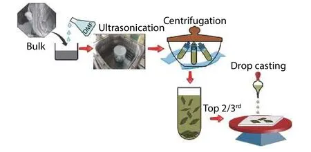
Fig.1.(Color online) Schematic diagram for synthesis of nanosheets and fabrication of thin films.
2.2.Characterizations
For the optical analysis, absorption spectroscopy (Perkin Elmer Lambda-35) in ultraviolet to visible range was carried out.Field emission scanning electron microscopy (FESEM, Hitachi SU 8010) and X-ray diffraction (XRD, PANalytical X’Pert Pro Diffractometer, Cu Kα,λ= 1.24 Å) were performed for the morphology and structural analysis.
3.Theory and calculations
Except from being an economical and simple technique,UV–visible spectroscopy provides a platform to thoroughly understand the optical behavior of a material and its comprehensive analysis.In this work, we have investigated the absorbance spectroscopy of TMDs, by illuminating in the ultraviolet to visible energy range of the electromagnetic spectrum.With the help of the absorbance spectrum, various optical parameters and their variation with the incident energy has been evaluated.The theoretical aspects of this study are described below.
3.1.Optical constants
The capability of a material to absorb the electromagnetic radiation is given by its absorption coefficient which is calculated as:
whereAis absorbance anddis the thickness of film.
Similarly, the extinction coefficient can be calculated with the help of absorption coefficient as:
From the reflectance (R) of the material, we can calculate fundamental optical property i.e.refractive index (n)[11].

Eq.(3) is known as the Fresnel equation which further yields the optical dielectric constants consisting of real and imaginary part.They depend on the values of extinction coefficient and refractive index as follows:

3.2.Optical band gap energy & Urbach energy
Optical transitions take place in a material at a particular energy known as its optical band gap (Eg(opt)).Determining this parameter is vital to describe the transport mechanism and conduction process occurring inside the material.Taucet al.has given a theory which leads to accurate calculation ofEg(opt)by making use of the Tauc equation which states that[12]:

wherendetermines whether a semiconductor is direct (n=2) or indirect (n= 0.5).A Tauc plot is drawn between (αhν)nandhν.The portion of this plot which can be fitted into a straight line is extrapolated to meet the horizontal axis.The point of contact gives the value ofEg(opt).The measure of disorder in a material can be achieved via the Urbach Empirical Rule[13].It is defined for low photon energies and states that the absorption coefficient of a material abides by the following relationship:

whereEuis the Urbach energy.
Further mathematics yields:

Therefore, a plot of ln(α) vshνmust contain a linear portion whose slope is reciprocal of Urbach Energy (Eu).Euis a direct measure of extent of order in a material i.e ifEuis higher,then the disorder is more and vice-versa.Some physical parameters for thin films such as optical density and skin depth are also related to the optical constants evaluated above.
3.3.Skin depth, optical density and optical conductivity
Due to morphology, microstructure and varying density of the thin film, the amount of photons penetrating insidethe thin film varies with its thickness.This is called the skin effect and the value of thickness at which the number of photons falls to 1/e of its value on the surface of the film, at a particular energy, is known as skin depth (δ).It can be calculated as:
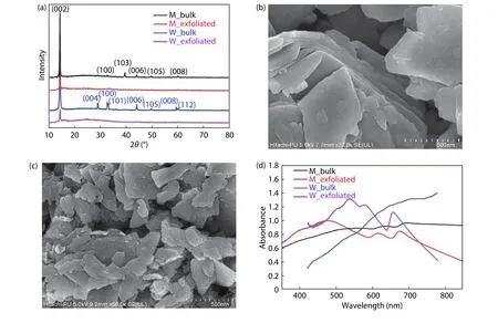
Fig.2.(Color online) Represents efficient exfoliation of bulk TMDs through (a) XRD spectra of MoS2, (b, c) FESEM of M_bulk and M_exfoliated, and(d) UV–visible spectra of all samples.
Another thickness-dependent parameter is optical density (O.D) given as:

The incident photons excite the electrons in the material depending upon their energy.The excited electrons are responsible for conduction and the resultant conductivity is termed as optical conductivity and denoted asσopt.It is related to the optical constants as follows:
wherecis the speed of light.
3.4.Dispersion energy parameters
A couple of models have been formulated to evaluate certain optical factors like dispersion energy (Ed), oscillator energy (Eo), oscillator strength (So) and oscillator wavelength(λ0).EoandEdare independent parameters which are related to the coordination number of the material and reveals information about the inclusive band configuration.The Wemple Di-Domenico model (WDM) states the dependence ofEoandEdon refractive index as follows[14]:

This can also be written in the form of a straight line:
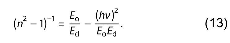
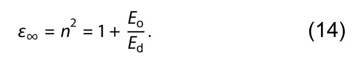
Therefore, a graph between (n2–1)–1and (hν)2gives the slope as 1/EoEdand intercept asEo/Edfrom whichEoandEdcan be calculated.The static refractive index (n0) and zero frequency dielectric (ε∞) are evaluated by equalizing (hν)2= 0 in Eq.(13):
Further,EoandEdpaves way for calculation of moments of spectraM–1andM–3as:

Another similar model developed by Sellmeier, known as the Single Sellmeier Model[14]provided the calculus to measureSoandλoby virtue of following mathematical statement:

Just like the previous model, the plot between (n2–1)–1andλ–2has slope = 1/Soand intercept 1/(Soλo2).Therefore,we can fetch the values ofSoandλofrom the slope and intercept.These parameters play a decisive role in fabrication and design of opto-electronic spectral devices.
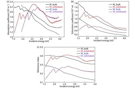
Fig.3.(Color online) Variation of (a) absorption coefficient, (b) extinction coefficient, and (c) refractive index with incident energy for all the samples.
4.Results and discussion
4.1.X-Ray diffraction (XRD)
We have used the XRD study as an initial tool to testify the purity and morphology of our prepared samples.The X-ray patterns of bulk and exfoliated counterparts of both MoS2and WS2are shown in Fig.2(a).In the case of MoS2, the XRD patterns are perfectly comparable with the JCPDS data 03-065-1951, which is indicative of the fact that no impurities were present in the samples.The bulk MoS2(M_bulk) shows peaks corresponding to (000), (100), (103), (106), (105), (008)out of which the (002) peak is the most intense.In contrast,(002) is the only peak which appears in the XRD of exfoliated MoS2(M_exfoliated) because exfoliation has occurred along the (002) plane.The prepared nanosheets have retained the crystallinity of its parent material but the stacking number is decreased as the characteristic (002) is broader and less intense in exfoliated material.This is consistent with the findings of other researchers in the past[15].FWHM (full width at half maximum) of M_exfoliated is augmented by 6° upon exfoliation, which, according to the Debye Scherer formula, gives the average stacking number as 3–4 layers[16].A similar trend is observed in the case of bulk WS2(W_bulk) and exfoliated WS2(W_exfoliated) samples (Fig.2(a)).Here, the XRD pattern matches well with JCPDS data 08-0237 and the exfoliated nanosheets show preferable orientation in the (002) direction.
4.2.Field emission scanning electron microscopy(FESEM)
Both MoS2and WS2films were characterized with FESEM to gain further insight into the contrast of lateral dimension and thickness of layers in bulk and exfoliated counterparts of both the materials.The image of M_bulk (Fig.2(b)) and M_exfoliated (Fig.2(c)) clearly present a reduction in stacking number and lateral flake dimension by delamination.A similar trend can be seen in WS2samples shown in Fig.S1 (Supplementary materials).
4.3.UV–visible spectroscopy
As mentioned in the theory, the absorbance of a material can be conversed to evaluate various optical constants,namely absorption coefficient (α), extinction coefficient (k),dielectric constants (εi&εr), refractive index (n) and optical conductivity (σopt) etc.The variation of absorbance with incident wavelength for MoS2and WS2are shown in Fig.2(d).In the case of W_bulk, there is no absorption peak observed but three visible excitonic peaks exist at 462, 521 and 629 nm in the spectra of W_exfoliated.
The absorbance spectra of M_bulk unveil excitonic peaks at 637 and 691 nm, respectively.These peaks are shifted towards decreasing wavelengths in the case of M_exfoliated with peak positions at 616 and 675 nm.This blue shift acknowledges a substantial fragmentation of thick flakes into few-layer nanosheets[17].
4.3.1.Assessment of optical constants
The potential of an optically active material is determined by its capability of absorption of light, which can be described by evaluation of optical constants likeαandk.Using Eqs.(1) and (2), the variation ofαandkwith incident energy for all the samples are shown in Figs.3(a) and 3(b).In the case of bulk samples (M_bulk & W_bulk), bothαandkdecrease with increasing incident energy.However, for M_exfoliated and W_exfoliated, there are augmented values at cer-tain points in the visible region of incident energy which signify maximas of absorption.High absorption at certain energies, make these materials advisable for opto-electronic applications.Further, with the values ofk, we calculated the refractive index (n) with the help of Eq.(3).It decreases with incident energy (or increases with incident wavelength) for bulk samples in the whole range of illumination depicting normal behavior of the dispersions (see Fig.3(c)).
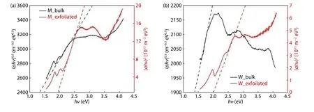
Fig.4.(Color online) Tauc plot for (a) M_bulk, M_exfoliated and (b) W_bulk, W_exfoliated.
Table 1.Optical band gap (Eg(opt)) and Urbach energy (Eu) for all the samples.
This is known as a “normal behavior”.On the other hand,refractive index is very sensitive to incident energy in exfoliated samples.In the lower energy region up to 2.5 eV, the dispersions behave anomalously, but in a higher energy range they behave normally[18].The peaks in reflectance spectra of M_exfoliated and W_exfoliated samples show spiked values of ‘n’ at certain values of energy.Such high values might be due to the equivalence between incident frequency and plasma frequency[19].The variation of optical conductivity,skin depth and optical density with the incident energy is shown in Figs.S2, S3 and S4 respectively.
4.3.2.Determination of optical band gap and Urbach Energy
To determine the optical band gap of a material, the method developed by Tauc was adopted.In the case of our samples, both MoS2and WS2clearly unveiled a transformation from indirect band gap semiconductor to a direct band gap semiconductor upon exfoliation (see Fig.4).The optical band gaps determined for all samples using Eq.(6) are summarized in Table 1.An optical band gap contrast (i.e.the difference betweenEg(opt)of bulk and exfoliated samples) of around 0.62 eV and of 0.64 eV has been found in MoS2and WS2samples respectively.This reassures that the band gap transitions lying in the UV–visible spectrum are responsible for semiconducting opto-electronic applications of such TMDs.The variation of ln(α) with incident energy is drawn in the low energy range in Fig.S5.The reciprocal of the slope of this graph gives the value ofEuwhich is calculated and listed in Table 1.
4.3.3.Dielectric constant
The comprehensive study of dielectric function is the foundation of profound understanding of optical phenomenon occurring in the material when it is excited with photon energy[20].Therefore, it is imperative to investigate this behavior for usefulness of TMDs in blooming opto-electronic technologies.The real and imaginary part of dielectric function has been calculated using Eqs.(4) and (5).It has been plotted against the incident photon energy for all the samples in Figs.5(a) and 5(b).The real part of dielectric constant rises with increasing frequencies of incident radiation which implies that the dielectric polarization induced in the material is more at higher energies.The increment in polarization effects is due to elevated density of states at higher frequencies.Moreover, it can be clearly observed from Figs.5(a) and 5(b) that in the visible domain, M_exfoliated and W_exfoliated reveal stronger and blue shifted polarization peaks as compared to their corresponding bulk counterparts.The contrast in dielectric behavior accounts for a greater optical contrast arising due to curtailed dimensions of nanosheets.In contrast, the imaginary dielectric constant shows reversing trends as expected.This signifies weaker polarization and greater optical loss as we increase the incident energy in all the samples.
4.3.4.Wemple Di-domenico model (WDM)
The optical analysis of any material that finds applications in the electromagnetic spectral range devices is incomplete without evaluation of dispersion energy and oscillator energy parameters.By using the values of refractive indices in Eq.(13), a variation of (n2–1)–1vs (hν)2has been plotted according to WDM (see Figs.5(c) and 5(d)).The linear portion of the graph gives the values of slopes and intercepts which further yield the WDM parameters.Further, the relationship between (n2–1)–1vsλ–2(Fig.S6) yields the SSM parameters using Eq.(17).The parameters are summarized in Table 2.Few more vital parameters were calculated using Eqs.(14)–(16).These are moments of spectra, static referactive index and zero frequency dielectric constant respectively.
5.Conclusion
Extensive optical study has been performed on MoS2and WS2TMDs in both bulk and nanomaterial morphologies.The“multilayer” to “few-layer” transformation was achieved with the liquid exfoliation process.The resulting nanosheet dispersions were drop-casted onto quartz substrates for further investigations.Several initial tests like XRD and FESEM were carried out to assure the successful exfoliation.UV–visible spectroscopy served as the major tool to thoroughly examine the optical response of TMDs from ultraviolet to visible range of frequencies.Beginning with the absorbance spectra, various optical constants were calculated and their variation with incident energy has been explained.The data was fitted with WDM and SSM models to evaluate dispersion energy and oscillator energy parameters.The performance statistics of nanosheets have been found to be greatly enhanced as compared to the bulk counterparts.This exclusive analysis is novel to TMDs, as there is no clear distinction between the optical parameters of bulk and nanosheets reported so far, to our knowledge.The spectral variation of optical constants can help in understanding a particular optical phenomenon and makes way for more suitable applications in photonics and electronics.For example, the presence of sharp excitation peaks at certain values of incident energies can be useful in creating excitation wavelengths.

Fig.5.(Color online) Variation of (a) real part and (b) imaginary part of dielectric constant with incident energy for all samples.WDM plots for (c)M_bulk, M_exfoliated and (d) W_bulk, W_exfoliated.
Table 2.Dispersion energy and oscillator energy parameters for all the samples.
Acknowledgements
We would like to acknowledge SAIF, CIL, Panjab University, Chandigarh, for the characterization facilities and the Department of Physics, Panjab University, Chandigarh, for laboratory equipments.
Appendix A.Supplementary materials
Supplementary materials to this article can be found online at https://doi.org/1674-4926/42/8/082001.
