Low-cost dual-stage offset-cancelled sense amplifier with hybrid read reference generator for improved read performance of RRAM at advanced technology nodes
2021-08-26QiaoWangDonglinZhangYulinZhaoChaoLiuXiaoxinXuJianguoYangandHangbingLv
Qiao Wang, Donglin Zhang, Yulin Zhao, Chao Liu Xiaoxin Xu, Jianguo Yang,and Hangbing Lv
1Institute of Microelectronics of Chinese Academy of Sciences, Beijing 100029, China
2University of Chinese Academy of Sciences, Beijing 100049, China
3Zhejiang Lab, Hangzhou 311121, China
Abstract: In this work, two process-variation-tolerant schemes for a current-mode sense amplifier (CSA) of RRAM were proposed: (1) hybrid read reference generator (HRRG) that tracks process-voltage-temperature (PVT) variations and solve the nonlinear issue of the RRAM cells; (2) a two-stage offset-cancelled current sense amplifier (TSOCC-SA) with only two capacitors achieves a double sensing margin and a high tolerance of device mismatch.The simulation results in 28 nm CMOS technology show that the HRRG can provide a read reference that tracks PVT variations and solves the nonlinear issue of the RRAM cells.The proposed TSOCC-SA can tolerate over 64% device mismatch.
Key words: RRAM; double sensing margin; device mismatch cancellation; nonlinearity of RRAM resistance; hybrid reference-cell
1.Introduction
Resistive random access memory (RRAM) has been studied as a promising candidate for the next generation of embedded non-volatile memory due to its advantages such as high scalability, low power consumption, high speed and non-volatility[1,2].However, the practical application of RRAM at advanced technology nodes is challenged by a limited sensing margin[3].The sense amplifier (SA) needs to tolerate the increasing mismatch of devices.A read reference that tracks process and temperature variations is also essential[4−6].Several offset-cancellation techniques have been proposed to reduce the device mismatch and improve the sensing margin[7−9].However, only the first stage (current-sampling) or the second stage (latch) of the SA was calibrated.In addition,multi capacitors in the offset-cancellation circuits also incur a remarkable area overhead.Moreover, the nonlinearity of RRAM cells has not been considered in previous dummy-cell read references.
In this work, a two-stage offset-cancelled current sense amplifier (TSOCC-SA) with only two capacitors is proposed.Two capacitors are used to maximize the sensing margin of RRAM and the tolerance of device mismatch.In addition, a hybrid read reference generator (HRRG) is designed by combining RRAM cells and linear resistors to provide a read reference that can track PVT variations and solve the nonlinear issue of the RRAM cells.
2.RRAM cell and its nonlinearity
The structure of the 1T1R RRAM cell used in this study includes an NMOS switch transistor and a TaOx-based bipolar resistor memory device.Fig.1 shows the cross-section transmission electron microscope (TEM) images of the fabricated RRAM cells in the 28 nm CMOS process.The RRAM is fabricated at the back end of line (BEOL) process and is fully compatible with the logic process[10].
The schematic of the 1T1R RRAM cell is shown in Fig.2, including the word line (WL) used to select the cell, and the bit line (BL) and source line (SL) used to apply the corresponding operation voltage.A fresh RRAM cell is in an initial state with extremely high resistance[11]and requires a one-time forming process to form a large number of conductive filaments (CFs) as shown in Fig.2(a).After the forming process,the RRAM cell is in a low resistance state (LRS) as shown in Fig.2(b).The reset operation is shown in Fig.2(c).A reset voltage (VReset) is applied to the RRAM cell from the SL to BL.The reset operation ruptures the formed CFs, making the RRAM cell from the LRS to the high resistive state (HRS).In the set operation, a set voltage (VSet) is applied to the RRAM cell from the BL to SL and CFs form again to make the cell into an LRS[12].
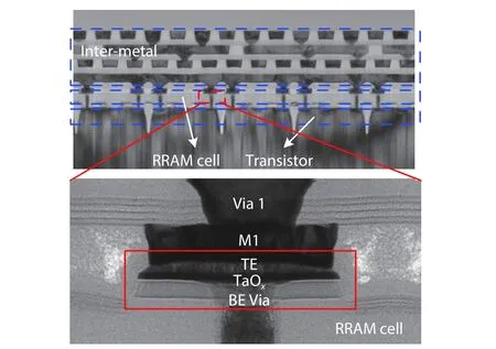
Fig.1.The TEM images of 1T1R RRAM cells.
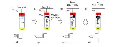
Fig.2.(Color online) RRAM cell basic operations: CFs forming, Reset and Set.
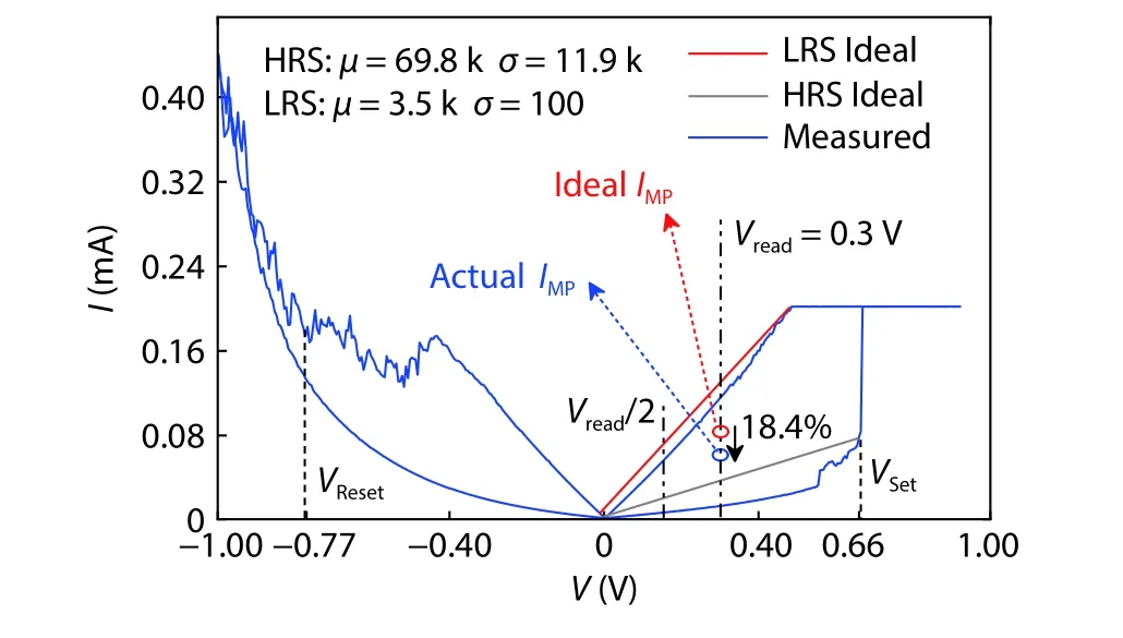
Fig.3.(Color online) Measured I–V curve and ideal I–V curve of RRAM cell.Ideal IMP is the mid-point current of the ideal value of IHRS and ILRS.Actual IMP is the mid-point current of the measured value of IHRS and ILRS.The actual IMP is 18.4% lower than the ideal IMP.

Table 1.RRAM cell operating conditions.
In the read operation, a small read voltage (Vreadis much lower than set voltage) is applied to the BL and then the CSA detects the current in the read path to determine the state of the cell resistance.TheVreadapplied to the BL will cause the migration of a small number of oxygen atoms.Then the distribution of oxygen vacancies inside the RRAM cell is changed and the resistance of RRAM cells exhibits nonlinearity.As shown in Fig.3, the ideal linearI–Vcurve of HRS and LRS is not exactly consistent with the measuredI–Vcurve.
Table 1 shows the operating conditions of the 1T1R RRAM cell used in this study.The RRAM cell has a large resistance variation (R-variation).R-variation leads to the wide distribution of cell current (Icell) and references current (Iref) that will cause sensing yield issues[13].Therefore, for an SA, a read reference that tracks process and temperature variations is essential.
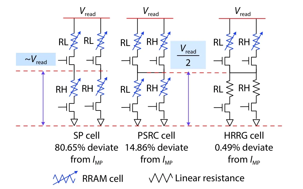
Fig.4.(Color online) Reference cell structure diagrams for SP scheme,PSRC scheme and HRRG scheme.
3.Hybrid read reference generator
The previous dummy reference cell structures of the Serial-Parallel (SP) scheme[14], Parallel-Series Reference Cell (PSRC)scheme[15], and the proposed hybrid read reference generator (HRRG) are shown in Fig.4.The HRRG adopts the Parallel-Series structure like the PSRC scheme.Besides, several dynamic-reference sensing schemes have been proposed to maximize the sensing margin[16−18].Nevertheless, the dynamic-reference sensing schemes are always accompanied by higher power consumption and area overhead.
The average of HRS RRAM cell and LRS RRAM cell is used as the reference in the SP scheme, and theIspis as Eq.(1).

Fig.5 shows the simulated reference current (Iref) distributions of conventional reference schemes and the proposed hybrid read reference, not considering the nonlinearity of the RRAM cell.The ideal reference for CSA should be the midpoint current of the two neighboring memory states (IMP).The reference current generated by SP schemes is closer to the current of HRS (IHRS) and the existing overlap may cause sensing failure with PVT variations.The reference current generated by PSRC (IPSRC) and the proposed HRRG (IHRRG) is in the middle ofIHRSandILRS, as shown in Eq.(2).
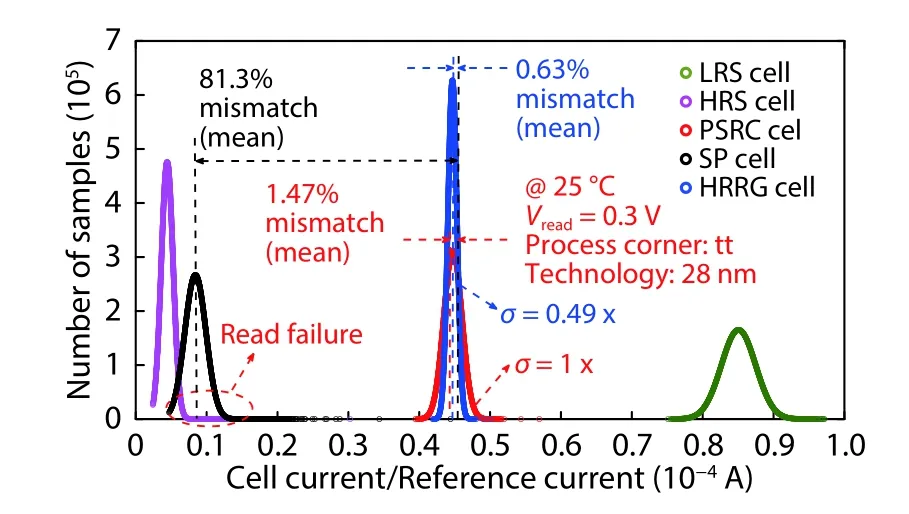
Fig.5.(Color online) The distributions of cell current and the reference current.
This is very close to the ideal reference for the CSA.In addition, as shown in Fig.5, the HRRG can achieve a narrower distribution compared with the PSRC.Specifically, the HRRG reduces theσ-IREFby 49% compared with the PSRC scheme.The difference between the proposed HRRG and the previous PSRC scheme is that the pair of parallel RRAM cells in the PSRC scheme is replaced by linear resistors to solve the nonlinear issue of RRAM cells, as shown in Fig.4.The two linear resistors are trimmed close to HRS and LRS of RRAM cells, respectively.Assuming that the four linear resistors are used in HRRG, the reference current with the most narrower distribution range can be obtained.However, it will not be able to track the PVT variations of the RRAM cell.
As shown in Fig.3, the resistance of the RRAM cell is nonlinear.The voltage falling on two pairs of parallel resistors is aboutVread/2 according to Ohm’s law.Therefore, the expression of the actual currents of the PSRC scheme and the HRRG scheme can be described as Eq.(3).

Taking into account the nonlinearity of the RRAM cell,Fig.3 shows the measuredILRSandIHRSwhich are 25% and 70% lower than the ideal value at a read voltage of 0.3 V, respectively.Hence, the actual value of theIMPis 18.4% lower than the ideal value of theIMP.TheIPSRCis 14.86% higher than the actual value of theIMPcalculated from theI–Vcurve in Fig.3.By contrast, the proposedIHRRGis only 0.49% higher than the actual value of theIMP.
Using the proposed HRRG scheme, the reference current shows a more concentrated distribution and is more agreed with the true value ofIMP.Hence, the sensing margin is maximized and the accuracy of the reading is improved.Moreover,the latency of the CSA with HRRG is minimum compared with the CSA with SP or PSRC, as shown in Fig.6.
4.Two-stage offset-cancelled current sense amplifier
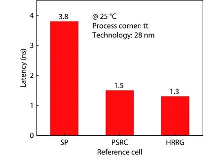
Fig.6.(Color online) The maximum latency of the CSA with different reference cells.
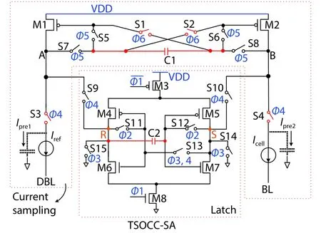
Fig.7.(Color online) Schematic diagram of TSOCC-SA.
A two-stage offset-cancelled current sense amplifier(TSOCC-SA) with only two capacitors is proposed to improve the sensing margin.Fig.7 shows the schematic of TSOCC-SA.The TSOCC-SA is comprised of a current-sampling and a latch.Compared to the previous OCCS-SA in Ref.[7], the proposed TSOCC-SA uses two cross switches (S1 and S2) for offset-cancellation.The switches (S3 and S4) are used to enlarge the sensing margin.Combined with the use of switches S1, S2, S3, and S4, only one capacitor can realize the function in Ref.[7], which significantly reduces the area of the circuit.The offset cancellation of the second stage of TSOCC-SA is realized by using a similar scheme proposed by Dong[8].
Fig.8 shows the timing of TSOCC-SA.In P1, the outputs of the two inverters are connected to their inputs, respectively.The difference between the trip voltages of the two inverters (VTR–VTL) is sampled by capacitor C2.In P2, the outputs of the two inverters are reset to “0”.And, the input of the right inverter becomes “VTR–VTL” while that of the left inverter remains “0”.In P3, two diode-connected transistors(M1 and M2) supply pre-charge currents (Ipre1andIpre2) to A and B nodes.After a sufficient pre-charge time, the currents of M1 and M2 (IM1andIM2) decrease to nearIrefandIcell, regardless of the device mismatch in M1 (M2) as long asIcellandIrefare constant in P3.Finally, the gate voltages (VG1andVG2) of M1 and M2 are stored at the left and right ends of capacitor C1, respectively.In P4, the four switches (S5–S8) are turned off and the two switches (S1 and S2) are turned on.The A (B)node has a current path to GND through S3 (S4), resulting in strong positive feedback.In P5, the latch comparator starts to work and outputs “1” or “0”.
Fig.9 shows the simulated waveforms of the CSB-SA[9]and the proposed TSOCC-SA.TSOCC-SA has a substantial influence on the sensing margin and performance.In P3, the operations of the CSB-SA and the TSOCC-SA are exactly the same.Four switches (S1–S4) are turned on at the beginning of P3,and the CSB-SA samplesIcellandIrefthrough these switches.Similarly, the TSOCC-SA samplesIcellandIrefthrough six switches (S3–S8).In P4, the operations of the CSB-SA and the TSOCC-SA are different.In the CSB-SA, the four switches(S1–S4) are turned off at the beginning of P4.However, in the TSOCC-SA, the double sensing margin switches (S1–S4) are turned on, and the four switches (S5–S8) are turned off.In the CSB-SA, without discharge path, bothVAandVBin P4 monotonically increase until one of them reaches VDD.In the TSOCC-SA, the M1 (M2) charges the A (B) node with the sampled currentIcell(Iref), while the S3 (S4) discharges the A(B) node with the currentIref(Icell).Thus, the current difference between the A and B nodes in the TSOCC-SA is twice that of the CSB-SA.
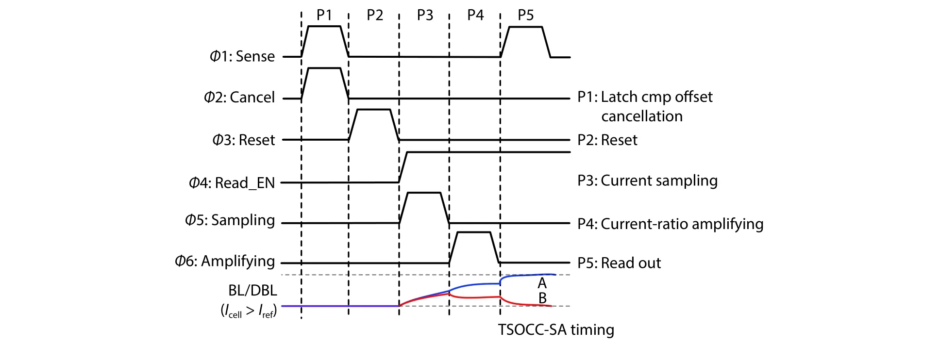
Fig.8.(Color online) The timing of TSOCC-SA.
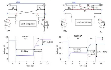
Fig.9.(Color online) CSB-SA and proposed TSOCC-SA.Bit-cell state 1 (Icell > Iref) is assumed in the VA and VB waveforms.
Fig.10(a) shows the sensing margin development withVTHmismatch between M1 and M2.For TSOCC-SA, when the device mismatch reaches 64% of the threshold voltage, the sensing margin is still enough, and the sense amplifier is valid.It clearly shows that the TSOCC-SA has higher offset-tolerance than the CSB-SA in Ref.[9].And the TSOCC-SA can work at a lower operation voltage to reduce power consumption by introducing offset-cancellation techniques, as shown in Fig.10(b).In addition, when the mismatch between M1 and M2 exceeds 225 mV, the swing between A and B is lower or even only tens of millivolts.Then, the mismatch between M4 and M5, M6 and M7 in the latch comparator will lead to the invalidation of SA.Hence, it is extremely necessary to introduce the cross-coupling capacitor C2 in the latch comparator to cancel these device mismatches, which can further improve the accuracy of SA.Donget al.have proved that the standard deviation of the mismatches is reduced by more than 60% by C2[8].
Moreover, the TSOCC-SA avoids excessive area overhead.In the layout, the area of the coupling capacitor is equivalentto that of a transistor.Fig.11 shows the sensing margin of several offset-cancellation techniques (CSB-SA[9], OCCS-SA[7],SCOC-SA[8], and TSOCC-SA) and the extra area overhead caused by the coupling capacitor.

Fig.10.(Color online) (a) Simulated ∆V [= min |VA –VB|]and ∆I [= min |IA –IB|]vs.VTH mismatch between transistors M1 and M2.(b) The maximum VTH mismatch that can be tolerated by TSOCC-SA at different operation voltage.

Fig.11.(Color online) The extra area overhead and sensing margin of several offset-cancellation techniques.
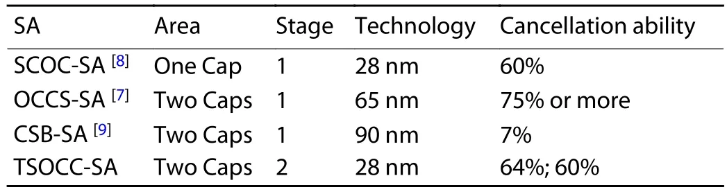
Table 2.Performances of several offset-cancellation techniques.
Table 2 shows the performance comparison of several offset-cancellation techniques.The area is characterized by the number of coupling capacitors (Caps).Stage indicates that the mismatch of how many stages of SA can be cancelled.Cancellation ability indicates the percentage of the mismatch voltage to the threshold voltage that can be tolerated by SA.
5.Conclusion
In this paper, we proposed a two-stage offset-cancelled current sense amplifier (TSOCC-SA) with only two capacitors for RRAM at an advanced technology node.A hybrid read reference generator (HRRG) is designed by combining RRAM cells and resistors to provide a read reference that tracking PVT variations and to solve the nonlinear issue of the RRAM cells.The simulation results in the 28 nm CMOS process have proved the effectiveness of HRRG and the reliability of the TSOCC-SA.
Acknowledgements
This work was supported in part by the National Key R&D Program of China under Grant No.2019YFB2204800 and in part by the Major Scientific Research Project of Zhejiang Lab(Grant No.2019KC0AD02) and in part by the National Natural Science Foundation of China under Grants 61904200 and the Strategic Priority Research Program of the Chinese Academy of Sciences under Grant No.XDB44000000.
