Influence of the finite size effect of Si(001)/SiO2 interface on the gate leakage current in nano-scale transistors
2019-10-15LiHaixiaJiAimingZhuCanyanMaoLingfeng
Li Haixia Ji Aiming Zhu Canyan Mao Lingfeng
(1School of Rail Transportation, Soochow University, Suzhou 215006, China)(2School of Information Engineering, Suqian College, Suqian 223800, China)(3School of Computer & Communication Engineering, University of Science & Technology Beijing, Beijing 100083, China)
Abstract:With the device size gradually approaching the physical limit, the small changes of the Si(001)/SiO2 interface in silicon-based devices may have a great impact on the device characteristics. Based on this, the bridge-oxygen model is used to construct the interface of different sizes, and the finite size effect of the interface between fine electronic structure silicon and silicon dioxide is studied. Then, the influence of the finite size effect on the electrical properties of nanotransistors is calculated by using the first principle. Theoretical calculation results demonstrate that the bond length of Si-Si and Si-O shows a saturate tendency when the size increases, while the absorption capacity of visible light and the barrier of the interface increase with the decrease of size. Finally, the results of two tunneling current models show that the finite size effect of Si(001)/SiO2 interface can lead to a larger change in the gate leakage current of nano-scale devices, and the transition region and image potential, which play an important role in the calculation of interface characteristics of large-scale devices, show different sensitivities to the finite size effect. Therefore, the finite size effect of the interface on the gate leakage current cannot be ignored in nano-scale devices.
Key words:finite size effect; tunneling current; nano-scale transistor
With the development of technology, the demand of improved performance in the semiconductor transistor has required reducing the device’s dimension in recent years, which follows a well-known scaling law known as “Moore’s law”. The size of the device is further reduced to its physical limit, and the research of small size effect is essential[1-2]. The dominance of Si in microelectronics is largely based on the high quality of the interface between Si and its native oxide SiO2[3].Many studies have been devoted to replacing SiO2with high-k gate dielectrics. However, in the case of high-k gate dielectrics, very thin SiO2is unavoidable[4-5]. Si- and SiO2-based systems also have the advantage of low cost as well as dealing with abundant, nontoxic, stable and durable materials. Therefore, many experiments and theoretical verifications on Si/SiO2interface have been carried out[6-12]. However, the precise bonding information remains controversial[12-15].

1 First Principle Method
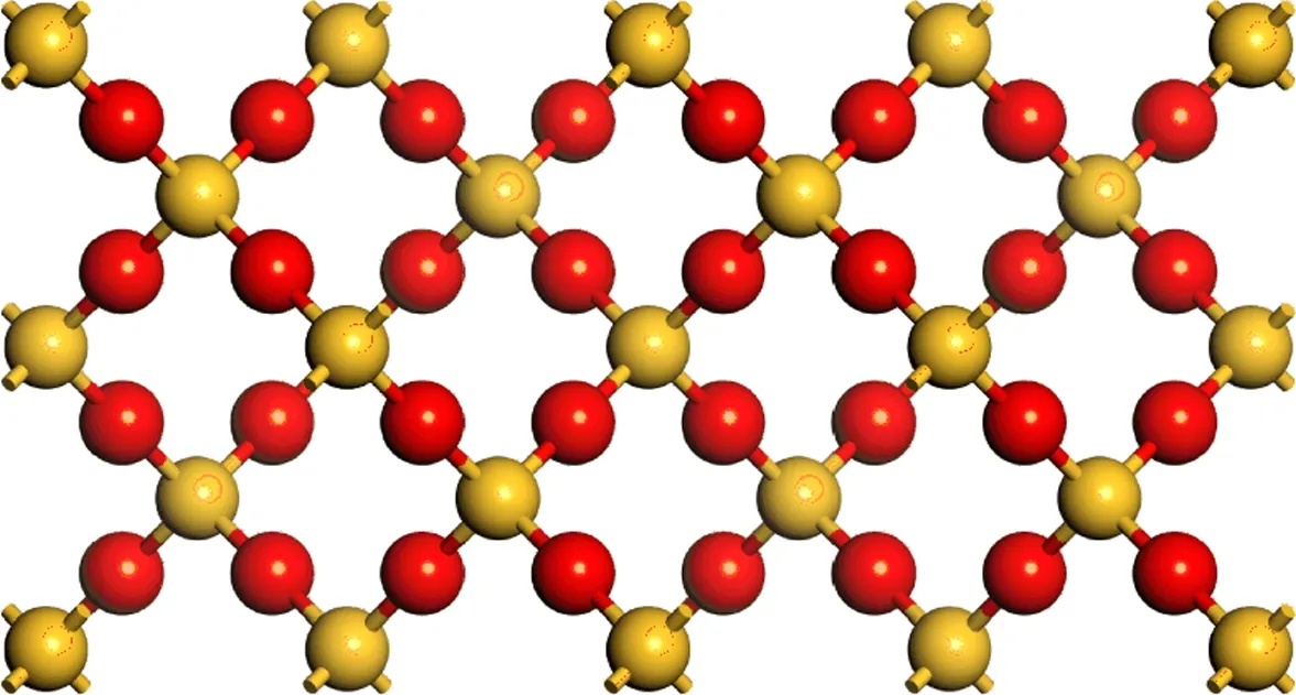
The interface model used in this paper is the bridge-oxygen model (BOM), which is first put forward by Herman et al[32]. It is the simplest and most suitable model for electronic structure calculation[33-36]. This model consists of two layers of Si(see Fig.1 (a)) and two layers of idealized β-cristobalite SiO2(see Fig.1 (b)). The experiment lattice constants are 0.543 and 0.716 nm for Si and SiO2, respectively. The lattice mismatch rate is 32%. The mismatch can be reduced to less than 7% by rotating SiO2by an angle of π/4, as shown in Fig.1(c). The BOM interface dangling bonds are saturated by adding an oxygen atom to bridge the two Si bonds. Here, the Si-O-Si angle is 144° and the length of Si-O bonds is 0.202 nm. The resulting unit cell has 72 atoms (47 Si and 25 O atoms)and dimensions of 0.5431 nm in theX-Yplane and 2.5181 nm in theZ(growth) direction. To ensure the independence of the interface, a 0.5 nm vacuum layer is added. Finally, the interface structure is obtained in Fig.1(d). No cell optimization of the model has been carried out.
In order to study the characteristics of the interface in nano-scale transistor considering the finite size effect, six structures with different sizes are constructed, as shown in Fig.2.
The geometrical optimization and energy calculations are performed using the CASTEP (Cambridge serial total energy package) program[37], which employs the plane pseudopotential method to calculate the total energy within the framework of the Kohn-Sham DFT. The PBE (Perdew, Burke, Ernzerh) formulation of the generalized gradient approximation (GGA) is always used to describe exchange correlation energy[38]. The Vanderbilt ultra-soft pseudo potential is used, which allows numerically converged calculations at relatively low kinetic energy cutoffs of the plane wave basis. The Broyden, Fletcher, Goldfarb and Shanno (BFGS) algorithm is applied to optimize the model structures. The convergence criteria for the self-consistent field (SCF) energy and the displacement are set to be 2.0×10⁻⁶eV/atom and 2×10⁻⁴nm. 2×5×1 k-point meshes are taken in the Brillouin zone, and the ground state energy is calculated with the Pulay density mixed method under the following conditions: The precision is 1.0×10⁻⁵eV/atom, and the cutoff energy of the plane wave is 340 eV.
Using the DFT theory, the effect of dimensional changes on the characteristics has been studied. Jie et al.[39]used CASTEP to study the influence of GaSe layer variation on optical properties. Niedfeldt et al.[40]also reported the influence of different cell sizes.
2 Results and Discussion
2.1 Electronic structure
It has been pointed out that the change of Si layer will affect the properties of silicon-based devices[41]. Therefore, the influence of the variedw/ton the Si-Si and Si-O bond length in the interface is first calculated.
Fig.3 shows the average bond length of Si-Si and Si-O. As seen from Fig.3, the average bond length of Si-Si gradually decreases with the increase inw/t, and finally tends to be saturated. On the other hand, although the Si-O bond length increases with the increase inw/t, it also finally tends to be saturated. These results show that the interface structure tends to be stable due to the influence of the surface state and quantum size effect with the increase inw/t[42].The relative change of the Si-Si bond length achieved 3.16%, and the Si-O bond length is as high as 4.53%. Such a large change is very important to the nano-scale transistor. From Fig.3, we conclude that the finite size effect can be ignored when the width is up to 2 nm and above when the oxide thickness is 2.5 nm.
2.2 Optical properties
By analyzing the electronic structure of the interface, it is found that the increase inw/twill affect the bond length of the Si side. The change of the structure in the Si side will inevitably affect the optical properties of the interface[41]. The dielectric function is the bridge between the microphysical processes of interband transitions and the electronic structure of materials.ωis the independent variable of the complex dielectric function,ε(ω)=ε1(ω)+iε2(ω),ε1(ω) is the real part andε2(ω) is the imaginary part of the dielectric function. It mainly represents the transition between the occupied and non-occupied states of electrons, and other spectral information can be easily obtained from it. Therefore, the imaginary part of the dielectric function and the other optical parameters are calculated and analyzed.
The changes in the imaginary part of dielectric function under different ratios ofw/tare given in Fig.4. It can be seen that the absorption peak shifts to the left and the peak value decreases gradually with the increase inw/t.
Fig.5 shows the variation of absorption peak with the increase inw/t. It can be seen that the absorption peak shifts to the left and decreases gradually with the increase inw/t. It indicates that with the increase inw/t, the absorption of photon energy in the high-energy region becomes weaker due to the influence of the surface effect and the quantum size effect. By comparing structure a with structure f, the absorption peak has decreased by almost an order of 10-1. This property can be used to control the optical properties of the transistor.
The change of optical properties with ratiow/twill lead to the change of electronic properties of devices. Therefore, we next investigate the tunneling current of the nano-scale transistor consisting of the Si/SiO2interface with differentw/t.

(a)
(b)

(c)

(d)

(a)

(b)

(c)

(d)

(e)

Fig.3 The average bond length of Si-Si and Si-O for the six nano-sizes

(a)

(b)
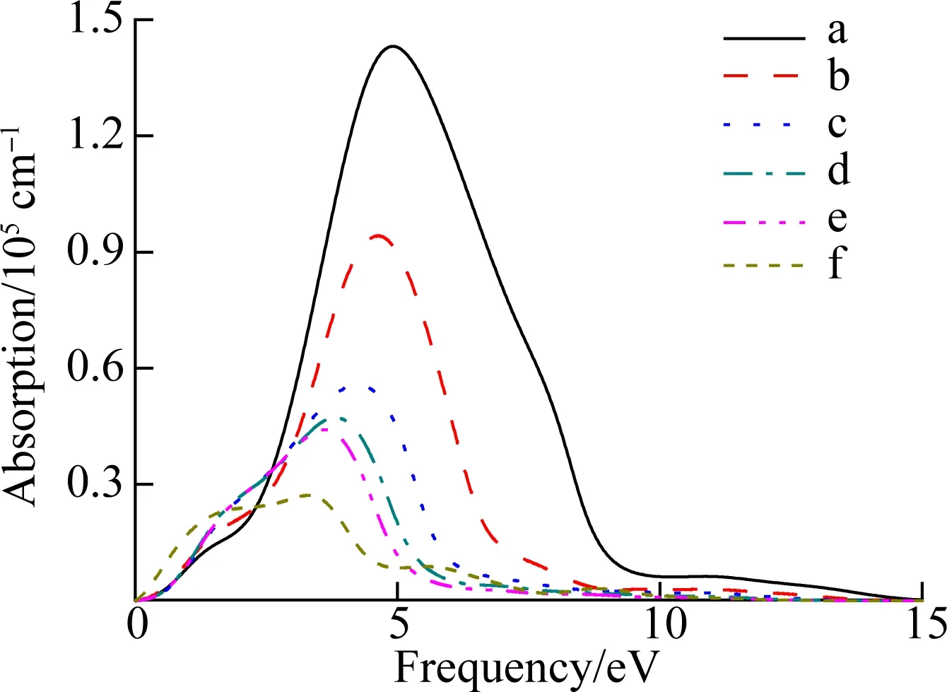
Fig.5 The size dependence of the absorption in Si/SiO2 interface
2.3 Energy band profile
2.3.1 Planar microscopic potential via first principles
The valence band profiles are calculated using the average potential method[43]. The electrostatic potential for the super cell is averaged in theX-Yplane; then, a planar microscopic potential is calculated in theZdirection.
(1)
At the Si/SiO2interface, the band changes continuously from Si to SiO2(see Fig.6). The coordinatesZ1,Z2are corresponding to the transition region boundaries andDis the width of the transition region. Before the calculation of transistor characteristics, the definition of the transition region is very important. The coordinates in theZdirection, corresponding to the band profile changes in a trend away from the averages and vice versa, are set to be the interface region boundaries. For example, the band goes up away from its average at pointAin Fig.6, so the coordinateZ1corresponding to pointAcan be set to be a boundary for the interface structure. Similarly, the other boundary can be set atZ2. After measurement, we can obtain the width of the transition region, which isD=Z2-Z1=0.48 nm. This result is consistent with others reported[16,26,36,44-45]and it is also in agreement with the measured results in the laboratory[46]. By measuring the potential of the structure with six nano-sizes (see Fig.2) in this paper,Dremains unchanged at different ratios ofw/t.

Fig.6 The planar microscopic potential along the Z direction
We can measure the VBM for the six structures with different sizes in Fig.6, and further obtain the CBM of these structures. The barrier heights are shown in Fig.7 which are calculated according to Fig.6. It can be seen clearly that the barrier height curve shows a downward trend, and the trend is getting slower. It is clear that the tunneling current will increase with the increase inw/tdue to the reduction of the barrier height.

Fig.7 The barrier height for the six nano-sizes
2.3.2 Gate tunneling current
Ando and Itoh[47]presented a numerical calculation method for gate leakage current with two tunneling conditions:
(2)
(3)
whereVoxis the voltage added to the barrier layer, and the electric field in the oxide isEox=Vox/Tox.Toxis the oxide thickness.BandCare given, respectively, by
(4)
(5)

The above classical tunneling current formulae approximately consider the interface region to be abrupt, and do not consider the influence of image potential. However, it can be clearly seen that the potential changes in the interface are not abrupt as shown in Fig.6. On the other hand, it will reduce the area and the thickness of the barrier due to the existence of the image potential. This will cause an increase in the tunneling current. Furthermore, when the oxide layer becomes ultra-thin and the applied voltage is below the potential barrier height, the classical FN formula is not applicable[48].
Taking the transition region (widthD) into account, the FN tunneling current through a triangular barrier can be rewritten as[49]
(6)
where
(7)
Taking the effect of barrier lowering induced by image potential into account, the direct tunneling (DT) current can be rewritten as[48]
(8)
Using Eq.(6), the FN tunneling current considering the transition region can be obtained in Fig.8(a). It shows the FN tunneling current under different applied voltages across gate oxide with different ratios ofw/t. It can be seen that the tunneling current increases gradually with the increase in the ratio, but the trend of the increase decreases, which is corresponding to the observed electronic structure (see Fig.3). In Fig.8(b), the change in the ratio ofJtrans/Jtrans0as a function of the applied gate voltages is calculated, whereJtrans0is the FN tunneling current without the finite size effect. The FN tunneling current becomes larger considering the finite size effect than that without considering. The ratio decreases with the increase in the electric field of the oxide layer. When the electric field is 10 MV/cm, the ratio ofJtrans/Jtrans0is up to 45 for structures with different sizes. However, when the field increases to 20 MV/cm, the ratio is only 4. Clearly, the FN tunneling current will increase due to the finite size effect. The increased amount becomes smaller when the electric field is increased.
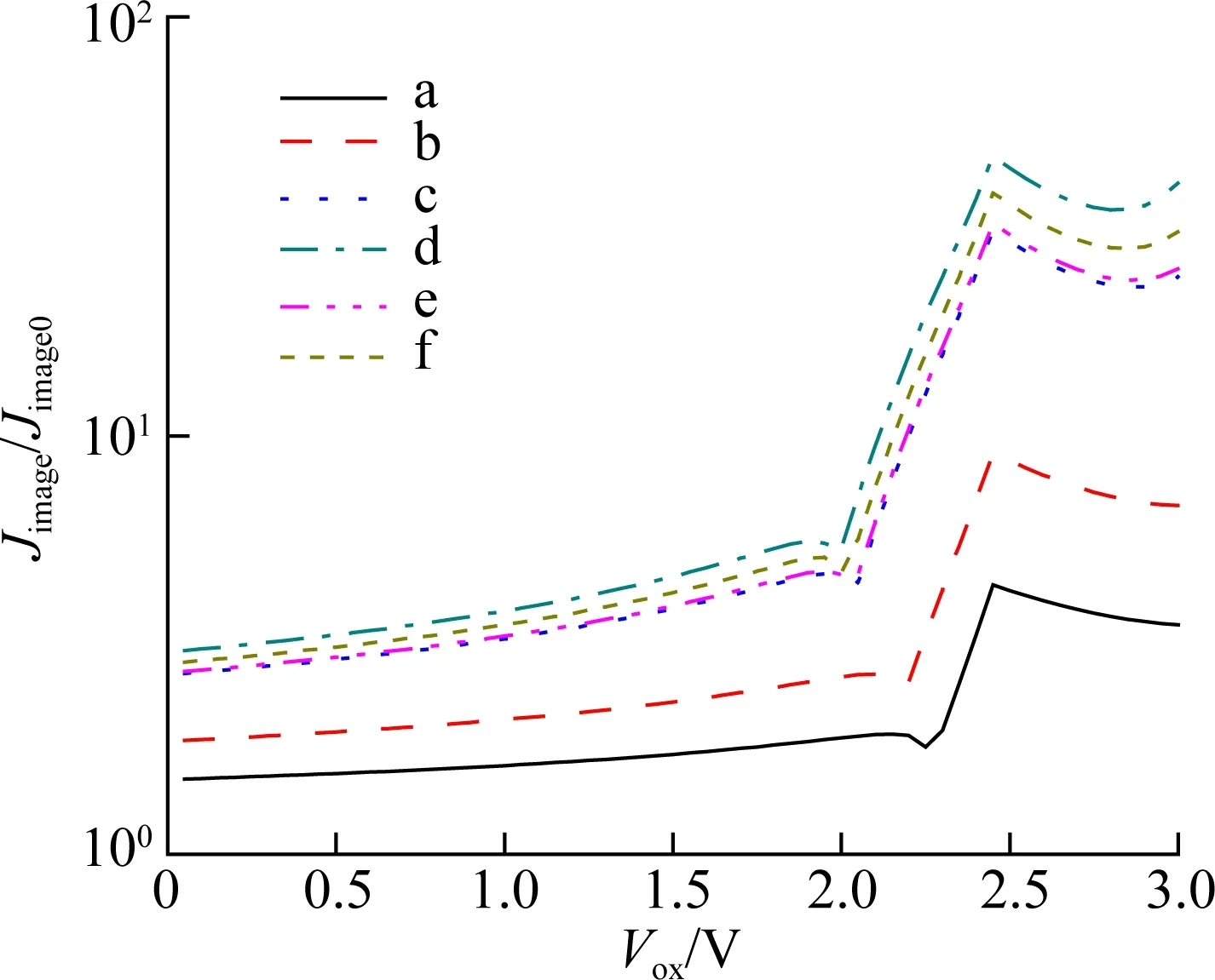
Fig.9(a) shows the change ofJimage, which is calculated using Eq.(8). It can be seen that the direct tunneling current already exists in the low voltage region which is different from the FN tunneling current. The direct tunneling current will increase with the increase inw/t. We can also see that the currents have an obvious turning point in the high voltage region, and the current increases significantly after the turning point. In an ultra-thin gate transistor, the gate field will increase with the decrease of the gate thickness, which corresponds to the high voltage region in which the direct tunneling current is significantly increased. Through this result, we find that the effect caused by sizes cannot be ignored as the size of the transistor decreases.

(a)

(b)
Fig.9(b) shows the change in the ratio ofJimage/Jimage0, whereJimage0is the direct current without the finite size effect. It can be seen that the direct current will increase due to the finite size effect. It also shows that with the increase in gate voltage, there are two turning points in the current curve. When near the FN tunneling area, the influence of the finite size effect is almost saturated and declines. This indicates that the influences of the finite size effect on the direct tunneling and FN tunneling are different. When the electric field is 10 MV/cm, the ratio ofJimage/Jimage0is only 3 for structures with different sizes. We can conclude that the finite size effect has a greater impact on the FN tunneling current than on the direct tunneling current.
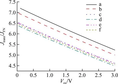
Figs.10(a) and (b) show the changes in the ratios ofJtrans/JFNandJimage/JDT, whereJFNis the tunneling current without the transition region, andJDTis the direct tunneling current without considering the effect of image potential. It can be seen that both the tunneling current will increase with the transition region and image potential. However, the existence of the finite size effect has redu-ced the influence of the transition region and image potential, and leads to a decrease in the ratio ofJtrans/JFNandJimage/JDT, separately. It also shows that with the increase in gate voltage, bothJtrans/JFNandJimage/JDTwill gradually decrease.

(a)
(b)
Fig.11(a) shows the change in the ratio ofJtrans/JFN, in which the currents are calculated under different gate voltages and oxide thicknesses when the barrier height isφ=3.15 eV. It can be seen that the influence of the transition region on the tunneling current decreases with the increase in the gate voltage under the same oxide thickness. Furthermore, the degree of decline will gradually increase with the decrease of the oxide thickness. The ratio ofJtrans/JFNdecreases from 7.8 to 4.5 withTox=1 nm when the gate voltage changes from 0 to 3 V. On the other hand, the ratio decreases from 7.8 to 6.8 withTox=3.5 nm when the gate voltage changes from 0 to 3 V. This is because with the decrease in thickness, the transition region occupies a larger proportion of the whole interface region. Therefore, considering the transition region or not will produce a greater impact on the tunneling current when the oxide thickness is smaller.
Fig.11(b) shows the change in the ratio ofJimage/JDTunder different gate voltages and oxide thicknesses, separately. Comparing Fig.11(a) and (b), we find that alth-ough the ratio is greater for direct tunneling current than for the FN tunneling current at the same oxide thickness and same gate voltage, the variation trend is similar, which is consistent with the numerical results obtained by Mao et al[48].Jimage/JDTdecreases with the increase in gate voltage. We also conclude that considering the image potential or not will produce a greater impact on the tunneling current when the oxide thickness is smaller. The ratio ofJimage/JDTdecreases from 21.6 to 9.7 when the gate voltage changes from 0 to 3 V. This ratio is lower than that of FN tuneling which is shown in Fig.11(a). These results indicate that the direct tunneling current is more dependent on oxide thickness than on the FN tunneling current.
(a)

(b)

(b)
It has been pointed out that the threshold voltage modulation of an MOSFET is affected not only by the channel length of the transistor, but also by its channel width[50]. The conclusions of this paper are consistent with the experimental conclusion that the leakage current becomes larger when the channel width increases[51].
Fig.12(a) shows the change of FN tunneling current calculated by Eq.(6) with different oxide thicknesses and applied gate voltages. It can be clearly seen that the tunneling current increases with the decrease of oxide thickness when the same gate voltage is applied. The dependence on the thickness of the oxide layers is greater while the gate voltage is smaller. Also, we conclude that under the same oxide thickness, the tunneling current decreases rapidly with the decrease of the gate voltage, and the tunneling current of FN is almost ignorable in the low voltage region (the current ranges from the magnitude of the 10-4to the order of magnitude of 10-36). This is consistent with the conclusion obtained by Yeo et al[52].

(a)
Fig.12(b) shows the variation of the direct tunneling current under different gate voltages and oxide thicknesses, and the barrier reduction effect caused by the image potential is considered. It can be seen that the direct tunneling current reduces with the increase in the oxide thickness when the same gate voltage is applied. When the oxide thickness ranges from 1 to 4 nm, the direct tunneling current is reduced by 14 orders of magnitude when applied voltage is 2 V. The value is 11 when the applied voltage is 3 V. Under the same oxide thickness, the tunneling current increases with the increase in the gate voltage. It is also shown that the direct tunneling current cannot be ignored in a transistor with oxide thickness less than 3 nm.
These results indicate that the FN tunneling current is more dependent on the applied voltage across the gate oxide in the nano-scale transistor. We also conclude that when traditional methods such as increasing oxide thickness or reducing gate voltage are no longer useful for decreasing the leakage current, we can use the finite size effect to achieve this.
3 Conclusions
1) Both the bond length of the Si-Si and Si-O at the interface will be saturated when the interface size increases.
2) The finite size effect must be considered when the interface size is less than 2 nm. It can cause a change in the absorption spectrum of visible light. It implies that the absorption spectrum of visible light can be used as a tool to characterize the interface size.
3) When the device is nanoscale, the barrier height of Si/SiO2decreases with the decrease of the interface size.
4) The tunneling current is significantly changed due to the finite size effect. It is well known that the existence of the transition region and image potential will cause a greater tunneling current. However, the increasing ratio will be weakened by the finite size effect.
5) This work can help us to clarify the impact of the finite size effect of the Si/SiO2interface on tunneling current in nano-scale transistors. Not only can we better understand the characteristics of the interface, but also help to optimize the parameters of the next generation of nano-transistors in the future.
杂志排行

Journal of Southeast University(English Edition)的其它文章
- Tensile behaviors of ecological high ductility cementitious composites exposed to interactive freeze-thaw-carbonation and single carbonation
- Delay-performance optimization resource scheduling in many-to-one multi-server cellular edge computing systems
- Image denoising method with tree-structured group sparse modeling of wavelet coefficients
- Travel time prediction model of freewaybased on gradient boosting decision tree
- Projection pursuit model of vehicle emission on air pollution at intersections based on the improved bat algorithm
- Experimental investigation of oil particles filtration on carbon nanotubes composite filter