中高温GaN插入层厚度对蓝光LED光电性能的影响
2017-01-05刘青明卢太平朱亚丹董海亮赵广洲周小润翟光美贾志刚马淑芳薛晋波李学敏许并社
刘青明, 卢太平*, 朱亚丹, 韩 丹, 董海亮,尚 林, 赵广洲, 赵 晨, 周小润, 翟光美, 贾志刚,梁 建, 马淑芳, 薛晋波, 李学敏*, 许并社
(1. 太原理工大学 新材料界面科学与工程教育部和山西省重点实验室, 山西 太原 030024;2. 太原理工大学 新材料工程技术研究中心, 山西 太原 030024)
中高温GaN插入层厚度对蓝光LED光电性能的影响
刘青明1,2, 卢太平1,2*, 朱亚丹1,2, 韩 丹1,2, 董海亮1,2,尚 林1,2, 赵广洲1,2, 赵 晨1,2, 周小润1,2, 翟光美1,2, 贾志刚1,2,梁 建1,2, 马淑芳1,2, 薛晋波1,2, 李学敏1,2*, 许并社1,2
(1. 太原理工大学 新材料界面科学与工程教育部和山西省重点实验室, 山西 太原 030024;2. 太原理工大学 新材料工程技术研究中心, 山西 太原 030024)
利用金属有机气相化学沉积(MOCVD)技术在蓝宝石图形衬底上生长GaN基蓝光LED,并系统研究了不同中高温GaN插入层厚度对其光电性能的影响。利用芯片测试仪和原子力显微镜(AFM)表征了GaN基蓝光LED外延片的光电性能以及表面形貌。当中高温GaN插入层厚度从60 nm增加至100 nm时,V形坑尺寸从70~110 nm增加至110~150 nm。当注入电流为20 mA时, LED芯片的光功率从21.9 mW增加至24.1 mW;当注入电流为120 mA时, LED芯片的光功率从72.4 mW增加至82.4 mW。对V形坑尺寸调控LED光电性能的相关物理机制进行了分析,结果表明:增大V形坑尺寸有利于增加空穴注入面积和注入效率,进而提高LED器件的光功率。
氮化镓; LED; V形坑; 空穴注入效率
1 引 言

在MOCVD外延过程中,超晶格的In组分对温度较为敏感,导致产品的一致性不能得到很好的保证;而且超晶格的生长速度较慢,亦会导致外延成本增加。与超晶格工艺相比,通过改变中高温GaN插入层厚度来控制V形坑尺寸的方法更具可行性,其生长工艺较为简单,生长速率更快,更有利于控制产品成本。本文通过控制中高温GaN插入层厚度来调控V形坑的尺寸,并对V形坑的形成机制以及载流子输运机理进行了讨论。实验结果表明,增大V形坑尺寸可以提高空穴的注入效率,进而提高LED的光功率以及外量子效率。
2 结果与讨论
图1为蓝宝石图形衬底上生长的GaN基蓝光LED外延结构示意图,样品A的中高温GaN插入层厚度为60 nm,样品B为100 nm。
图2为室温下样品A、B在注入电流为20 mA时测得的EL光谱。样品A、B的峰值波长和半高宽分别为454.1 nm和22.6 nm、455.0 nm和24.2 nm。以上数据表明:当中高温GaN厚度从60 nm增加至100 nm时,LED外延片的峰值波长红移0.9 nm,半峰宽展宽1.6 nm,EL积分强度增加约11.5%,这可能与插入层厚度增加、V形坑尺寸变大、载流子注入效率增加、辐射复合效率得到提高有关[21-22]。

图1 蓝宝石图形衬底上生长GaN基蓝光LED外延结构示意图
Fig.1 Schematic epitaxial structure of GaN-based blue LEDs grown on patterned sapphire substrate

图2 样品A、B在20 mA注入电流下的EL光谱。
图3为样品A、B的I-V曲线。在注入电流为20 mA时,样品A、B的正向偏压分别是3.18 V和3.13 V;在注入电流为120 mA时,样品A、B的正向偏压分别为4.35 V和4.25 V。实际二极管可以看作一个理想二极管和等效电阻串联而成,其电压-电流方程[23]可近似写成:
(1)
其中I为输入电流,Is为反向饱和电流,q为电子电荷,V为输入电压,R为等效串联电阻,n为二极管理想因子,k为玻尔兹曼常数,T为热力学温度。为方便描述,上述公式可变形为:
(2)

图3 样品A、B的I-V曲线。
经计算,样品A、B的串联电阻分别为9.2 Ω和8.1 Ω。即随着中高温GaN插入层厚度增加,样品B的正向偏压和串联电阻均变小,这可能与V形坑的尺寸变化有关。若V形坑尺寸增大,载流子注入效率增加,则正向偏压降低,串联电阻减小[24-25]。
图4是样品A、B的峰值波长和半峰宽随注入电流的变化图。由图4可知,随着注入电流的增加,峰值波长先蓝移后轻微红移,半高宽逐渐展宽。当注入电流从1 mA增加至40 mA时,样品A、B的峰值波长分别从459.2 nm蓝移至452.7 nm, 458.9 nm蓝移至454.7 nm,分别蓝移了6.5 nm和4.2 nm。样品B的蓝移量较小,这可能与V形坑尺寸变大、量子阱内应力变小有关[21]。当注入电流从40 mA增加至120 mA时,样品A、B的峰值波长由于热效应而产生轻微红移。随着注入电流从1 mA增加至120 mA,载流子的注入效率逐渐增加,能带填充效应增强,引起半峰宽展宽[22,26]。在同一注入电流下,样品B的半峰宽大于样品A,这可能与V形坑尺寸增大使载流子注入效率增加、能带填充效应更强有关(详细说明见图7)。

图4 样品A、B的峰值波长及半峰宽随注入电流的变化图。
Fig.4 Peak wavelength and full width at half maximum (FWHM) of sample A and Bvs. forward current
图5是样品A、B的光功率及外量子效率随注入电流的变化图。在相同注入电流下,样品B的光功率及外量子效率均大于样品A。当注入电流为20 mA时,样品A、B的光功率分别为21.9 mW和24.1 mW,样品B的光功率及外量子效率比样品A分别提高了10.0%和12.2%。当注入电流为120 mA时,样品A,B的光功率分别为72.4 mW和82.4 mW。样品B的光功率及外量子效率比样品A分别提高了13.8%和16.1%。这可能与中高温插入层厚度增加使V形坑尺寸增大、空穴注入效率提高有关(详细说明见图7)。
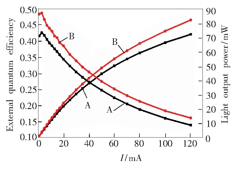
图5 样品A、B的光输出功率及外量子效率随注入电流的变化图。
Fig.5 Light output power and calculated EQE of sample A and Bvs. forward current
图6为样品A、B的AFM图像,扫描范围为2 μm×2 μm,扫描模式为轻敲模式。图像中均可观察到明显的二维台阶流生长模式,均存在较小黑点和较大六角形坑。其中较小的黑点为位错露头,较大的六角形坑为V形坑[27]。经统计,样品A的V形坑尺寸分布为70~110 nm,样品B为110~150 nm。这说明随着中高温GaN插入层厚度的增加,V形坑尺寸明显增大,这与之前通过改变超晶格周期数来控制V形坑尺寸的报道类似[20-21],但超晶格生长工艺对温度要求较为严格,生长速率也较慢,因此本文方法更具优势。

图6 样品A(a)、B(b)的AFM图像。
为更好地说明V形坑尺寸变化对LED光电性能的影响,图7给出了具有不同V形坑尺寸的GaN基LED的结构示意图。GaN基LED器件中V形坑形成原因主要有以下两点:一是外延层之间由晶格失配和热失配引起的应力会产生大量位错[28],在位错处易形成V形坑[29];二是低温生长时,Ga原子迁移能力较低,有效迁移时间较长,导致表面生长不平整而形成V形坑[30]。而在后续高温p-GaN生长过程中,参与生长的Ga原子能量增加,原子表面迁移率增大,有助于V形坑合并,从而形成平整的表面[17]。
与传统LED器件相比,含有V形坑的LED器件在空穴输运上有两大优势:第一,空穴注入面积占优。V形坑为倒金字塔结构,p型层面积大,n型层面积小,因此空穴在注入面积上占有优势。第二,空穴浓度占优。空穴在倒金字塔结构的V形坑中输运可能为压缩模式,即随着空穴往V形坑底部输运,运输面积逐渐减小,空穴浓度逐渐增高[17]。更重要的是,V形坑中的空穴还可通过侧壁量子阱注入到c面量子阱中。首先,V形坑内存在侧壁量子阱,侧壁量子阱中的In含量比c面量子阱低,故侧壁量子阱势垒高于c面量子阱,此高势垒可阻止空穴被位错等非辐射复合中心所捕获[19,31]。其次,侧壁量子阱较薄,只有c面量子阱厚度的1/3[15,32],在300 K下,空穴能量较高,较易从侧壁量子阱中隧穿至c面量子阱,从而提高了空穴注入效率,弥补了空穴在浓度上的不足,使得空穴与电子的浓度更为匹配[33-36]。
本文中的样品A和B,由于外延层中应力的积累以及Ga原子表面迁移率较低而在位错处形成V形坑(图7)。除中高温GaN插入层厚度不同外,样品A、B的其余生长工艺均一致,因此V形坑在中高温GaN插入层中产生的几何位置应该相当。由于样品B的插入层较厚,V形坑为倒金字塔结构,所以样品B中的V形坑尺寸较大,即空穴注入面积较大;更重要的是,样品B中的V形坑更深,因而由侧壁量子阱注入至靠近n-GaN 的c面量子阱中的空穴数目增多,使得空穴浓度分布更均匀,注入效率增加,电子和空穴的辐射复合效率得到提高[33-36]。这与本文中V形坑尺寸变大、正向偏压降低、光输出功率及外量子效率提高等结果相吻合。
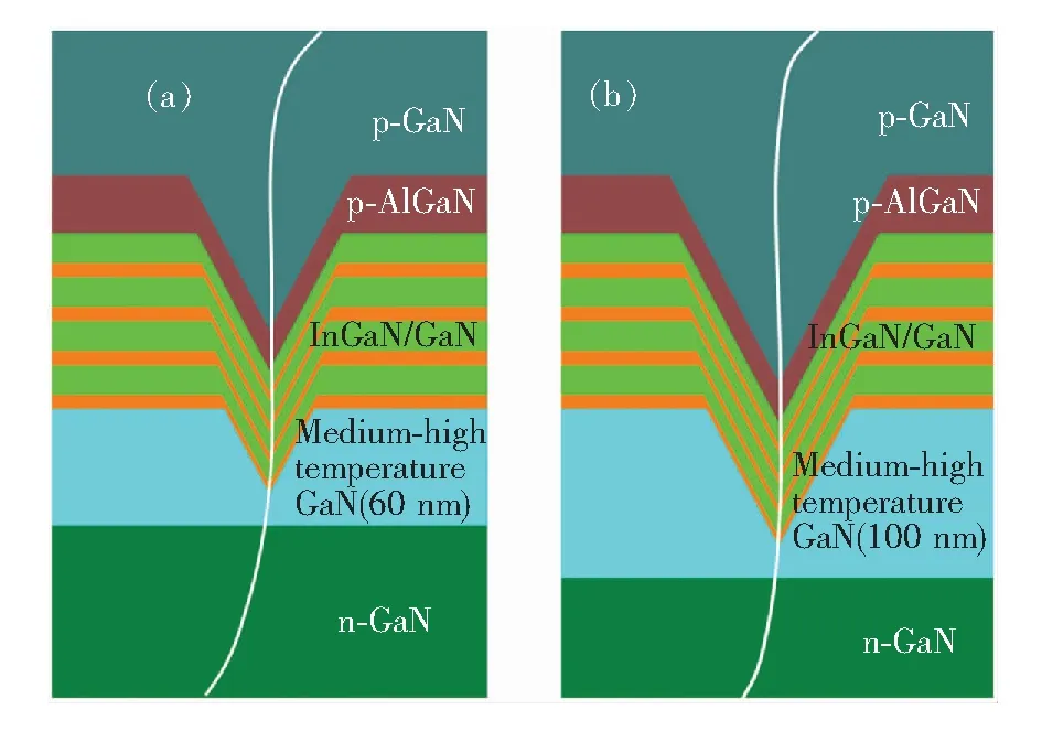
图7 具有不同V形坑尺寸的样品示意图。(a)样品A;(b)样品B。
Fig.7 Schematic of the epitaxial structure with different V-shaped size.(a) Sample A. (b) Sample B.
3 结 论
采用MOCVD法生长了具有不同厚度中高温GaN插入层的GaN基蓝光LED,通过调整GaN插入层的厚度来控制LED外延层中V形坑的尺寸。当中高温GaN插入层厚度从60 nm增加至100 nm时,V形坑尺寸从70~110 nm增加至110~150 nm。当注入电流为20 mA时,正向偏压从3.18 V降低至3.13 V,光输出功率提高了10.0%;当注入电流为120 mA时,光输出功率提高了13.8%。V形坑尺寸的增大可以使空穴注入面积增加,且V形坑深度的增加使空穴更易注入至靠近n-GaN的c面量子阱中,改善了c面量子阱中的空穴浓度分布,增加了空穴注入效率,提高了LED的光电性能。本文方法具有工艺简单、成本低廉的优点,更适合于工业化生产。
[1] DUPUIS R D, KRAMES M R. History, development, and applications of high-brightness visible light-emitting diodes [J].J.LightwaveTechnol., 2008, 26(9):1154-1171.
[2] LU T P, LI S T, ZHANG K,etal.. The advantage of blue InGaN multiple quantum wells light-emitting diodes with p-AlInN electron blocking layer [J].Chin.Phys. B, 2011, 20(9):098503-1-4.
[3] 李正凯,严启荣,罗长得,等. GaN垒层厚度渐变的双蓝光波长发光二极管 [J]. 光子学报, 2013, 42(7):757-762. LI Z K, YAN Q R, LUO C D,etal.. Dual-blue wavelength light-emitting diodes based on varied GaN barrier thickness [J].ActaPhoton.Sinica, 2013, 42(7):757-762. (in Chinese)
[4] SHANG L, LU T P, ZHAI G M,etal.. The evolution of a GaN/sapphire interface with different nucleation layer thickness during two-step growth and its influence on the bulk GaN crystal quality [J].RSCAdv., 2015, 5(63):51201-51207.
[5] NAKAMURA S, SENOH M, IWASA N,etal.. High-power InGaN single-quantum-well-structure blue and violet light-emitting diodes [J].Appl.Phys.Lett., 1995, 67(13):1868-1870.
[6] PEARTON S J, ZOLPER J C, SHUL R J,etal.. GaN: processing, defects, and devices [J].J.Appl.Phys., 1999, 86(1):1-78.
[7] LU L, GAO Z Y, SHEN B,etal.. Microstructure and origin of dislocation etch pits in GaN epilayers grown by metal organic chemical vapor deposition [J].J.Appl.Phys. 2008, 104(12):123525-1-4.
[8] BROWN P D. TEM assessment of GaN epitaxial growth [J].J.Cryst.Growth, 2000, 210(1-3):143-150.
[9] PONCE F A, MAJOR Jr J S, PLANO W E,etal.. Crystalline structure of AlGaN epitaxy on sapphire using AlN buffer layers [J].Appl.Phys.Lett., 1994, 65(18):2302-2304.
[10] LU T P, LI S T, LIU C,etal.. Advantages of GaN based light-emitting diodes with a p-InGaN hole reservoir layer [J].Appl.Phys.Lett., 2012, 100(14):141106-1-3.
[11] LIANG M M, WENG G E, ZHANG J Y,etal.. Influence of barrier thickness on the structural and optical properties of InGaN/GaN multiple quantum wells [J].Chin.Phys. B, 2014, 23(5):054211-1-5.
[12] PAN C C, YAN Q M, FU H Q,etal.. High optical power and low-efficiency droop blue light-emitting diodes using compositionally step-graded InGaN barrier [J].Electron.Lett., 2015, 51(15):1187-1189.
[13] CHUNG H J, CHOI R J, KIM M H,etal.. Improved performance of GaN-based blue light emitting diodes with InGaN/GaN multilayer barriers [J].Appl.Phys.Lett., 2009, 95(24):241109-1-3.
[14] 胡金勇,黄华茂,王洪,等. ITO表面粗化提高GaN基LED芯片出光效率 [J]. 发光学报, 2014, 35(5):613-617. HU J Y, HUANG H M, WANG H,etal.. Light-output enhancement of GaN-based light-emitting diodes with surface textured ITO [J].Chin.J.Lumin., 2014, 35(5):613-617. (in Chinese)
[15] HANGLEITER A, HITZEL F, NETZEL C,etal.. Suppression of nonradiative recombination by V-shaped pits in GaInN/GaN quantum wells produces a large increase in the light emission efficiency [J].Phys.Rev.Lett., 2005, 95(12):127402-1-4.
[16] CHICHIBU S F, UEDONO A, ONUMA T,etal.. Origin of defect-insensitive emission probability in In-containing (Al, In, Ga) N alloy semiconductors [J].Nat.Mater., 2006, 5(10):810-816.
[17] 吴小明. 含V形坑的Si衬底GaN基蓝光LED发光性能研究 [D]. 南昌:南昌大学, 2014. WU X M.StudyonTheLuminescencePropertiesofV-pit-containingGaNBasedBlueLEDsonSiSubstrate[D]. Nanchang: Nanchang University, 2014. (in Chinese)
[18] TOMIYA S, KANITANI Y, TANAKA S,etal.. Atomic scale characterization of GaInN/GaN multiple quantum wells in V-shaped pits [J].Appl.Phys.Lett., 2011, 98(18):181904-1-3.
[19] OKADA N, KASHIHARA H, SUGIMOTO K,etal.. Controlling potential barrier height by changing V-shaped pit size and the effect on optical and electrical properties for InGaN/GaN based light-emitting diodes [J].J.Appl.Phys., 2015, 117(2):025708.
[20] KIM J, CHO Y H, KO D S,etal.. Influence of V-pits on the efficiency droop in InGaN/GaN quantum wells [J].Opt.Express, 2014, 22(S3):A857-A866.
[21] SONG T L. Strain relaxation due to V-pit formation in InxGa1-xN/GaN epilayers grown on sapphire [J].J.Appl.Phys., 2005, 98(8):084906.
[22] LU T P, MA Z G, DU C H,etal.. Temperature-dependent photoluminescence in light-emitting diodes [J].Sci.Rep., 2014, 4:6131.
[23] CHEUNG S K, CHEUNG N W. Extraction of Schottky diode parameters from forward current-voltage characteristics [J].Appl.Phys.Lett., 1986, 49(2):85-87.
[24] QUAN Z J, WANG L, ZHENG C D,etal.. Roles of V-shaped pits on the improvement of quantum efficiency in InGaN/GaN multiple quantum well light-emitting diodes [J].J.Appl.Phys., 2014, 116(18):183107.
[25] HSU C C, WU C K, LI C K,etal.. 3D finite element strain analysis of V-shaped pits in light emitting diodes [C].ProceedingsofTheInternationalConferenceonNumericalSimulationofOptoelectronicDevices,ChinaTaipei:Taipei, 2015:7-8.
[26] ZHAO Y K, YUN F, WANG S,etal. Modulating dual-wavelength multiple quantum wells in white light emitting diodes to suppress efficiency droop and improve color rendering index [J].J.Appl.Phys., 2015, 118(14):145702.
[27] SCHENK H P D, VENNéGUèS P, TOTTEREAU O,etal.. Three-dimensionally nucleated growth of gallium nitride by low-pressure metalorganic vapour phase epitaxy [J].J.Cryst.Growth, 2003, 258(3-4):232-250.
[28] 郭瑞花,卢太平,贾志刚,等. 界面形核时间对GaN薄膜晶体质量的影响 [J]. 物理学报, 2015, 64(12):123705-1-6. GUO R H, LU T P, JIA Z G,etal.. Effect of interface nucleation time of the GaN nucleation layer on the crystal quality of GaN film [J].ActaPhys.Sinica, 2015, 64(12):123705-1-6. (in Chinese)
[29] SHIOJIRI M, CHUO C C, HSU J T,etal.. Structure and formation mechanism of V defects in multiple InGaN/GaN quantum well layers [J].J.Appl.Phys., 2006, 99(7):073505.
[30] SON K S, KIM D G, CHO H K,etal.. Formation of V-shaped pits in GaN thin films grown on high temperature GaN [J].J.Cryst.Growth, 2004, 261(1):50-54.
[31] WU X M, LIU J L, QUAN Z J,etal.. Electroluminescence from the sidewall quantum wells in the V-shaped pits of InGaN light emitting diodes [J].Appl.Phys.Lett., 2014, 104(22):221101-1-5.
[32] CAO X A, STOKES E B, SANDVIK P M,etal.. Diffusion and tunneling currents in GaN/InGaN multiple quantum well light-emitting diodes [J].IEEE.ElectronDev.Lett., 2002, 23(9):535-537.
[33] QUAN Z, LIU J L, FANG F,etal.. A new interpretation for performance improvement of high-efficiency vertical blue light-emitting diodes by InGaN/GaN superlattices [J].J.Appl.Phys., 2015, 118(19):193102.
[34] LI Y F, YUN F, SU X L,etal.. Deep hole injection assisted by large V-shape pits in InGaN/GaN multiple-quantum-wells blue light-emitting diodes [J].J.Appl.Phys., 2014, 116(12):123101.
[35] LI Y F, YUN F, SU X L,etal.. Carrier injection modulated by V-defects in InGaN/GaN multiple-quantum-well blue LEDs [J].Jpn.J.Appl.Phys., 2014, 53(11):112103.
[36] ZHAO Y K, LI Y F, HUANG Y P,etal.. Efficiency droop suppression in GaN-based light-emitting diodes by chirped multiple quantum well structure at high current injection [J].Chin.Phys. B, 2015, 24(5):056806-1-5.

刘青明(1990-),男,山东临沂人,硕士研究生,2012年于济南大学获得学士学位,主要从事GaN基蓝光LED外延及器件的研究。
E-mail: 497258449@qq.com

卢太平(1986-)男,重庆人,博士,讲师,2014年于中国科学院物理研究所获得博士学位,主要从事Ⅲ族氮化物外延生长以及微电子、光电器件的研究
E-mail: lutaiping@tyut.edu.cn

李学敏(1956-)男,美籍华人,博士,教授,1994年于美国里海大学获得博士学位,主要从事化合物半导体材料和器件开发及应用方面的研究。
E-mail: xueminli@tyut.edu.cn
Effect of Medium-high Temperature Interlayer Thickness on The Optical and Electrical Properties of Blue Light Emitting Diodes
LIU Qing-ming1,2, LU Tai-ping1,2*, ZHU Ya-dan1,2, HAN Dan1,2, DONG Hai-liang1,2, SHANG Lin1,2, ZHAO Guang-zhou1,2, ZHAO Chen1,2, ZHOU Xiao-run1,2, ZHAI Guang-mei1,2, JIA Zhi-gang1,2, LIANG Jian1,2, MA Shu-fang1,2, XUE Jin-bo1,2, LI Xue-min1,2*, XU Bing-she1,2
(1.KeyLaboratoryofInterfaceScienceandEngineeringinAdvancedMaterials,MinistryofEducation,TaiyuanUniversityofTechnology,Taiyuan030024,China;2.ResearchCenterofAdvancedMaterialsScienceandTechnology,TaiyuanUniversityofTechnology,Taiyuan030024,China)
GaN-based blue light emitting diodes (LEDs) were grown on patterned sapphire substrates by metal-organic chemical vapor deposition (MOCVD) method, and the medium-high temperature GaN interlayer with different thickness was grown between the multiple quantum wells layer and n-GaN layer. The Optical and electrical properties and surface morphology of LEDs were characterized by LED test system and atomic force microscopy(AFM), respectively. When the thickness of the medium-high temperature GaN interlayer increases from 60 nm to 100 nm, the size of V-pit enlarges from 70-110 nm to 110-150 nm. Meanwhile, the light output power of the chip increases from 21.9 mW to 24.1 mW with the injection current of 20 mA, and 72.4 mW to 82.4 mW with the injection current of 120 mA. In order to better illustrate the influence mechanism of the size of V-pits on the photoelectric properties of the LEDs, the schematic structures with different V-shaped pit sizes are demonstrated. The analyzing results for the LED samples show that the increase of the V-pit size is beneficial to enhance the hole injection area and injection efficiency. Thus, the light output power of the LED device is improved.
GaN; LED; V-pits; hole injection efficiency
2016-02-23;
2016-03-31
国家自然科学基金(21471111,61475110,61404089,61504090); 山西省基础研究项目(2014011016-6,2014021019-1,2015021103); 电子薄膜与集成器件国家重点实验室开放课题(KFJJ201406); 山西省科技创新重点团队项目(2012041011); 山西省高等学校科技创新项目(2015131); 浙江省重点科技创新团队(2011R50012); 浙江省重点实验室项目(2013E10022)资助
1000-7032(2016)07-0829-07
TN383+.1; TN364+.2
A
10.3788/fgxb20163707.0829
*CorrespondingAuthors,E-mail:lutaiping@tyut.edu.cn;xueminli@tyut.edu.cn