Recent development of transient electronics
2016-12-09HuanyuChengVikasVepachedu
Huanyu Cheng,Vikas Vepachedu
Department of Engineering Science and Mechanics,Materials Research Institute,The Pennsylvania State University,University Park,PA 16802,USA
Review
Recent development of transient electronics
Huanyu Cheng∗,Vikas Vepachedu
Department of Engineering Science and Mechanics,Materials Research Institute,The Pennsylvania State University,University Park,PA 16802,USA
H I G H L I G H T S
•A number of inorganic materials and their method of application were studied.
•Models of reactive diffusion were presented to predict the dissolution behavior.
•Various encapsulation approaches were explored as a way to extend the lifetime.
•The transient ECG sensor was configured in a stretchable layout.
A R T I C L EI N F O
Article history:
Accepted 26 November 2015
Available online 15 January 2016
Transient electronics
Model of reactive diffusion
Encapsulation strategy
Multilayer structures
Transient electronics are an emerging class of electronics with the unique characteristic to completely dissolve withina programmed periodof time.Sincenoharmful byproducts arereleased,theseelectronics can be used in the human body as a diagnostic tool,for instance,or they can be used as environmentally friendly alternatives to existing electronics which disintegrate when exposed to water.Thus,the most crucial aspect of transient electronics is their ability to disintegrate in a practical manner and a review of the literature on this topic is essential for understanding the current capabilities of transient electronics and areas of future research.In the past,only partial dissolution of transient electronics was possible, however,total dissolution has been achieved with a recent discovery that silicon nanomembrane undergoes hydrolysis.The use of single-and multi-layered structures has also been explored as a way to extend the lifetime of the electronics.Analytical models have been developed to study the dissolution of various functional materials as well as the devices constructed from this set of functional materials and these models prove to be useful in the design of the transient electronics.
©2016 The Authors.Published by Elsevier Ltd on behalf of The Chinese Society of Theoretical and Applied Mechanics.This is an open access article under the CC BY license(http://creativecommons.org/ licenses/by/4.0/).
Contents
1.Introduction........................................................................................................................................................................................................................21
2.Hydrolysis of semiconducting materials..........................................................................................................................................................................22
3.Model of reactive diffusion for transient materials.........................................................................................................................................................23
4.Dissolution of the device with bi-layered structures......................................................................................................................................................25
5.Conclusion..........................................................................................................................................................................................................................29
Acknowledgments.............................................................................................................................................................................................................30
References...........................................................................................................................................................................................................................30
1.Introduction
While the development of modern electronics has typically been concerned with durable devices that function stably over time,the advent of transient electronics takes an opposite approach;the destruction of the said devices is designed to provide unique opportunities.Upon exposure to water,transient electronics disintegrate at a predictable rate while releasing biologically and/or environmentally benign end products[1,2].This ability opensawiderangeofapplicationsfrombio-degradableelectronics to diagnostic/therapeutic implants[3,4].One can use an electronic component,for instance,as a temporary implant in a patient and allow it to safely dissolve on its own without the need for a second surgery[1,5].Ultimately,transient electronics can solve the problemofdisposingelectronicsinasafeandconvenientmanner[6–8].
The defining quality of transient electronics is their ability to dissolve into non-toxic products upon exposure to water and,naturally,dissolution accounts for a significant amount of research in this field[1,2,9–12].Early research on this topic resulted in achieving the partial dissolution of components through the use of organic materials as substrates[13,14].For instance,organic thinfilmtransistorshavebeendevelopedusingcotton-madepaper[15] as substrate and silk was also shown to be useful as a soluble substrate for implants in the body[16].However,this type of research was limited to the substrate and the electronic devices remained insoluble.
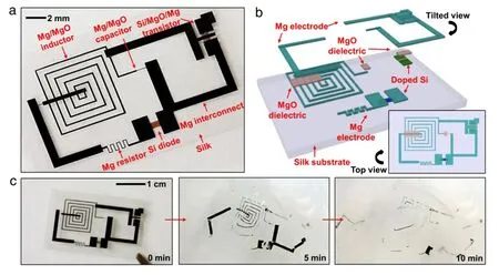
Fig.1.Proof-of-concept demonstration for transient electronics,with key materials and device structure layout.(a)Image of a device with all components deployed on a thin silk substrate.The device components include transistors,diodes,inductors,capacitors,and resistors,with interconnects and interlayer dielectrics.(b)Schematic illustration in an exploded view,with a top view in the lower right inset.(c)Images showing the time sequence at various dissolution stages in deionized(DI)water.
More recently however,electronics which are completely soluble have been developed.This relies on a recent,important discovery that semiconductor grade monocrystalline silicon can undergo dissolution in bio-fluids or even water at physiological conditions with a programmed lifetime relevant to applications in biomedicine[1].As the reaction rate of silicon hydrolysis to form silicic acid(Si(OH)4)is exceptionally small,silicon devices were fabricated in extremely thin forms.A nanomembrane of silicon with lateral dimensions similar to conventional circuits but with a thickness of 70 nm has been shown to dissolve in~10 days[1].Via similar chemistry,thin silicon dioxide(SiO2)was selected as a gate dielectric.Taken together with the other dissolvable,inorganic materials such as magnesium(Mg)and magnesium oxide(MgO) for conductors and the interlayer dielectric,respectively,due to their spontaneous reaction with water to form biologically benign Mg(OH)2,silicon nanomembranes provide a basic means for the construction of a transient,electronic device.As a proofof-concept,Fig.1(a)and(b)present a schematic demonstration platform which utilizes silicon nanomembranes(Si NMs)for the semiconductors,magnesium for the conductors,magnesium oxide and silicon dioxide for the dielectrics,and silk for the substrate and packaging materials.The collectively configured devices dissolve and disintegrate when immersed in DI water(Fig.1(c)).
Surface reactions typically dominate the dissolution behavior for sufficiently large reaction constants.The porosity of the materials(e.g.,Mg,MgO and SiO2)however,was found to be influential as it allows for the diffusion of water through the material,thereby increasing the dissolution rate through an increase in the effective surface area[12].In studying the dissolution of transient electronics,the factors to consider include physical and chemical properties of materials,and certain ambient factors of an aqueous environment.Given the research of these factors and others,analytical models have been developed to solidify the understanding of the dissolution behaviors in transient electronics[1,11,12].Such models can be of great assistance in the design of transient electronics.This review will first provide a comprehensive discussion on the hydrolysis of semiconducting materials with a focus on silicon nanomembranes,followed by the model of reactive diffusion to account for the dissolution behavior of porous materials.When combined with ideas from soft,tissuelike electronic devices,the class of transient electronics provides a viable means to monitor health or deliver care in a minimally obtrusive way.
2.Hydrolysis of semiconducting materials
To establish a realistic set of functional materials,knowledge regarding the chemical kinetics of each material is critical, especially that of the hydrolysis of semiconducting materials.At physiological pH levels and temperatures,the dissolution rates of semiconducting materials(e.g.,silicon,silicon–germanium,and germanium)are remarkably small[17].Therefore,in order to minimize the amount of semiconducting materials which must be dissolved,the nanomembrane structure is critical.Dissolution of monocrystalline silicon nanomembranes in phosphate buffered saline(PBS with pH=7.4)at biologically pertinent temperatures (e.g.,37°C)forms either an intermediate oxidation product SiO2or Si(OH)4through the equilibrium:Si+4H2O↔Si(OH)4+2H2[18,19].Theratedependsonthecrystalstructure,morphology,and doping concentration of silicon[20,21],as well as the temperature and composition of solutions[2,19].
Systematic characterization of the dissolution kinetics for siliconusedvariousbio-fluidsatmultiplepHlevelsandtemperatures. Patterned Si NMs(3µm×3µm×70 nm)were first created on a layer of thermal oxide on a silicon wafer,followed by immersion in aqueous buffer solutions(50 mL,in a petri dish with diameter of 7 cm).The dissolution rate of thermal oxide is negligible in comparison to that of silicon.Thicknesses of Si NMs were measured at a specific time(e.g.,every other day)after which the sample wasplaced into a fresh buffer solution.There was no significant change in the dissolution rate for a variety of time intervals(e.g.,for every 1,2,4,7 days),indicating accurate measurement in the dissolution rate.Studies of SiGe and Ge were given in a similar setup[17].Figure 2(a)presents atomic force microscope topographical images of a Si NM with an initial thickness of 70 nm collected at various stages of hydrolysis,demonstrating its transient behavior in biofluids(PBS with pH of 7.4;37°C).
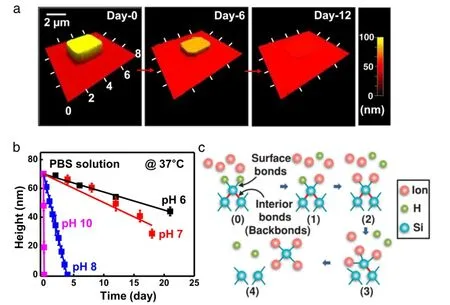
Fig.2.Experiments of silicon dissolution with corresponding theoretical and numerical analyses.(a)Atomic force microscope topographical images of a Si NM with initial dimension of 3µm×3µm×70 nm at various stages of hydrolysis in PBS at 37°C.(b)Theoretical(lines)and experimental(symbols)dissolution of Si NMs from(a)in buffer solutions at different pH levels(pH 6,black;pH 7,red;pH 8,blue;pH 10,purple),at physiological temperature(37°C).(c)Atomic configurations for each ion adsorption event in density functional theory(DFT)simulation of the silicon dissolution process.(For interpretation of the references to color in this figure legend,the reader is referred to the web version of this article.)
Given the dense arrangement of the silicon atoms in crystal structures,the hydrolysis of monocrystalline silicon nanomembranesislimitedtothesurfaceandthekineticscanbedescribedby a surface reaction with a constant dissolution rate[1,2].With the assumption that no solution molecules diffuse into the silicon,this modelyieldsalinearrelationshipbetweenthemeasuredthickness and the time,where the slopes represent the dissolution rates.A previously established empirical formula[19]suggests that an increase in the hydroxide ion concentration[OH−]results in an accelerated dissolution rate in high pH solutions of KOH.As shown in Fig.2(b),this formula can reproduce the experimental trends for solutions at the physiological pH levels if a different power law exponent is used for[OH−][2].


3.Model of reactive diffusion for transient materials
In addition to surface reactions,the diffusion in the porous materials cannot be ignored and the reaction between the diffused molecules and surrounding porous materials also needs to be considered.A model of reactive diffusion was proposed to analytically study the dissolution process of porous materials[23].Themodelconsidersthediffusionofwaterandhydroxideionsinto porous materials,which effectively increases the reactive surface. Here the key parameters are the diffusivity D of water in the porousmaterialandthereactionconstantkbetweenwaterandthe material.Becausetheinitialthicknessh0ismuchsmallerthanboth the width and length of the sample in the experiment,the onedimensional(1D)model can adequately capture the dissolution behaviors.Withy=0atthebottomofthemateriallayer(Fig.4(a)), the water concentrationw(y,t)at location y and time t satisfies the reactive diffusion equation[23]

This equation reduces to the standard diffusion equation if the reaction constant k is negligible.The boundary conditions of Eq.(1) include a constant water concentration at the water/porous material interfaceand a zero water flux at the porous material/substrate interface∂w/∂y|y=0=0.The initial condition is zero water concentrationIn order to transform the inhomogeneous boundary conditionto a homogeneous one,a new variableis introduced[12],which results in an updated equation

The boundary conditions and the initial condition becomeandrespectively.Eq.(2)is inhomogeneous,but the general solution can be represented by a sum of a homogeneous solutionθhand a particular solutionθp.The homogeneous solutionθhsatisfies the homogeneous equationwith homogeneous boundary conditionsand. Expressed in the form ofcan be solved by the method of separation of variables.The homogeneous equation leads towhereλis the eigenvalue to be determined from the boundary condition.The functions T(t)and Y(y)are then expressed as T=e−λtandwhere A and B are constants to be determined from initial and boundary conditions.Withandobtained from the homogeneous boundary conditions,A is solved to be A=0 and the trigonometric equationleads to the solution for eigenvaluesk(n=1,2,3,...),whichin turngivesthehomogeneous solution


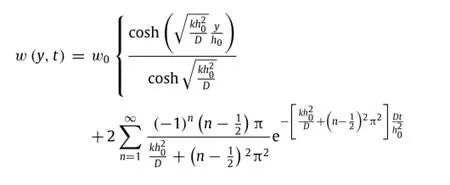

The solution given above indicates a clear scaling lawin which the normalized water concentrationw/w0depends on normalized position y/h0,normalized timeand a single non-dimensional parameterthat scales with the ratio of reaction constant k to diffusivity D.Experimental measurement of Mg with an initial thickness of 300 nm showsandwhich is within the range of reaction constants reported by Taub et al.[24].Figure 3(a)presents the distribution of water concentration for the normalized time0.2,0.4,0.8, 2 and∞,wherecorresponds to the steady-state limit of the water concentration in the Mg layerw(y,t→∞)=

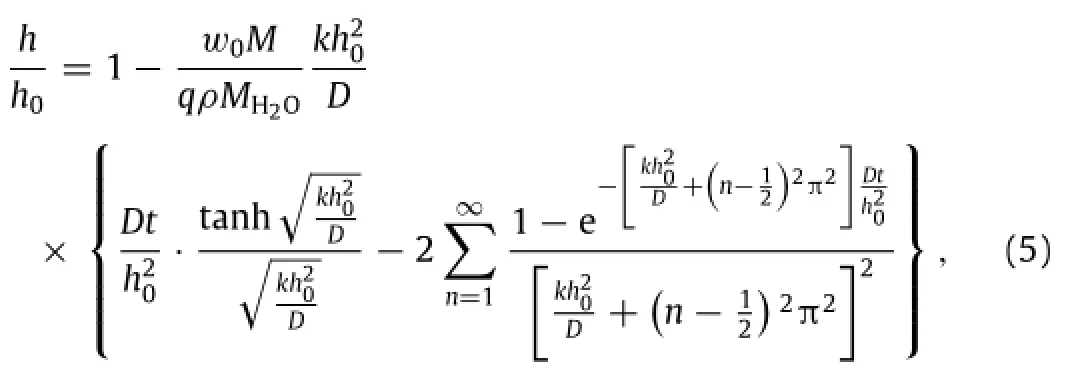
whereρis the mass density of the porous material.For parameters k and D relevant to applications of transient electronics in biomedicine,the summation on the right hand side of Eq.(5)is negligible in linear expression for the thickness as

is the critical time of complete physical disappearance for the transient material.The rate of dissolutionalso known as the electrical dissolution rate used for conductors[25],can be determined from the linear approximation of the thickness asThe rate of dissolution is 0.044 nm/s, 0.13 nm/s,and 0.20 nm/s for 100 nm-,300 nm-and 500 nmthick Mglayers,respectively.Thesequantitieshavethe same order of magnitude as rates of dissolution reported in the prior experiments[26,27].
The chemical reaction of Mg in phosphate buffered saline follows Mg+2H2O→Mg(OH)2+H2.Thus,two water molecules react with one Mg atom(i.e.,q=2).Because water molecules are the dominant molecule in phosphate buffered saline or the other bio-fluids,the water concentration is approximatelyw0= 1 g·cm−3.The critical time tcto dissolve Mg(molar mass M= 24 g·mol−1,mass densityρ=1.738 g·cm−3,and initial thickness h0=300 nm)is calculated as 38 min,which agrees reasonably well with the measurement of 40 min in the experiment.Via a similar chemistry,one silicon oxide atom reacts with two water molecules by SiO2+2H2O→Si(OH)4.Because the reactionbetween SiO2and water is much slower than between Mg and water(minutes to dissolve Mg versus days to dissolve SiO2),the reaction constant between water and SiO2(~10−6s−1)is much smaller than that between water and Mg(~10−3s−1).The rates of dissolution range from 0.11 to 0.47 nm/h for SiO2with an initialthicknessbetween35and100nmatatemperaturebetween room and physiological temperatures.These rates of dissolution for PECVD SiO2in water are consistent with the rates reported in priorexperiments[28],whicharehigherthanthoseforquartz[29].
In comparison to the intermittent thickness measurement, electrical properties can potentially provide continuous measurements.Electrical measurements also allow for evaluation of the dissolution behavior of a conductive material below a nonconductive layer,as discussed in the next section.The relative changes in both the width and length directions are much smaller than in the thickness direction.Therefore,the electric resistance is inversely proportional to the remaining thickness as R=R0h0/h≈R0/(1−t/tc),where R0is the initial resistance.Changes of resistance approximately account for both changes in thickness and influences associated with porosity,pitting and other nonuniformitiesinducedbynon-uniformdissolution[25].ThenormalizedelectricresistanceR/R0ofMgisshowninFig.4(c)asafunction of the normalized time t/tc.In this figure,the same reaction constant k=1.2×10⁻³s−1and diffusivity D=6.0×10⁻¹²cm2/s arechosenforMgwithan initialthicknessof300nmandinitial resistance(per unit length)R0of 1.06Ω/mm.It is important to note that an initial layer of thin MgO may exist on top of the Mg layer. In the presence of water,this thin MgO layer quickly reacts to form a more stable,crystalline hydroxide[30],which is not as protective as non-crystalline films[31].Thus,the single-layer dissolution model can properly account for the hydrolysis of Mg.
The potential of thin films made from other transient metals for use in transient electronics has also been explored and was found to be worth considering with the development of MOSFETs as an example[25].Analytical models discussed above are found to be applicable to other dissolvable metals,including Mg alloy, zinc(Zn),tungsten(W),and molybdenum(Mo).The prediction from the model can reproduce the observed dissolution behaviors inDIwaterandsimulatedbodyfluids(e.g.,Hanks’solutionwithpH from5to8)[25].Particularly,theelectricaldissolutionratesinthin films can be much different from traditionally reported corrosion rates in corresponding bulk materials.The model cannot,however, capture the dissolution behavior of iron(Fe),because Fe degrades in a spatially non-uniform manner,with certain reaction products (Fe2O3and Fe3O4)that have very low solubility[25].
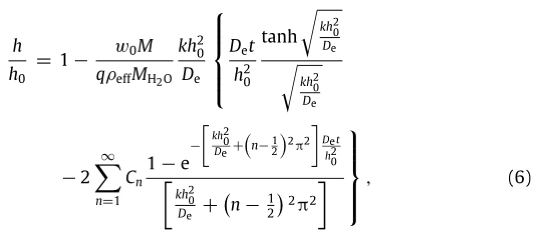
Silicon oxides and silicon nitrides are key materials for dielectrics and encapsulation layers in the class of silicon-based high performance electronics.The dissolution rates of these materials are affected by the physical and chemical properties of the films,which in turn depend on the deposition/growth methods and conditions.A key parameter that can approximately characterize these differences is density.The effects of density variation are two-fold.Reduced density increases the porosity in the porous materials,which results in an increased reactive surface to accelerate the dissolution.Secondly,it also reduces the amountofmaterialsthatneedtobedissolved.Theeffectivedensity ρeffof porous material is related to the densityρsof the fully dense materials asρeff= ρsVs/(Vs+Vair),where Vsand Vairare the volumes of the porous material and air cavity,respectively. A modified version of the reactive diffusion model provides a simple means to account for the density variation[11].In Eq.(1),the diffusivity D is replaced with an effective diffusivity De. The effective diffusivity of water in a porous medium is linearly proportional to the pore fraction in the porous medium:De∝Vair/(Vair+Vs)=(ρs−ρeff)/ρs.As densities of porous materials fromvariousdepositionmethods/conditionsaremeasureddirectly from the experiment,the effective diffusivity of water in each porous material can be determined.At time t=0,the air pores are filled with water,i.e.,w|t=0=w0(ρs−ρeff)/ρs(0≤y<h0). The boundary conditions remain the same as those for Eq.(1). Following the same approach discussed above,the normalized thickness is solved as[11]
4.Dissolution of the device with bi-layered structures
Applications in biomedicine require the transient electronics to function stably in a certain timeframe,followed by a complete physical disappearance.All of the transient materials however, start to dissolve immediately in the bio-fluids.The lifetime of the resulting devices is typically determined by Mg interconnects due totheirfastreactionwithwater.Althoughthesystemmayfunction before it completely breaks down,its performance is significantly compromised.Therefore,it is important to explore a mechanism that allows devices to function in a programmed lifetime.
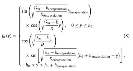
Adding encapsulation layers or packaging materials on top of the device can extend its lifetime in a controlled manner. For instance,MgO can serve as an encapsulation layer for Mg. In this bi-layered system(Fig.4(b)),zero initial condition at t=0 applies to both Mg and MgO layers.The reactive diffusion Eq.(1)together with zero water flux boundary condition at the bottom surface y=0 still holds for the Mg layer.As for the MgO encapsulation with an initial thickness ofthe reactive diffusion equation becomes[12]whereandare the diffusivity of water in MgO and reaction constant between MgO and water,respectively.The constant water concentration boundary condition at the MgO/water interface isIn addition,the continuity conditions of water concentration and flux across the MgO/Mg interface areandSimilar to the single-layer system,theinhomogeneous boundary condition leads to a representation of the water concentration as a sum of a homogeneous solutionwhand a particular solutionwp,i.e.,w=wh+wp.The homogeneous solutionwhsatisfies the homogeneous equationwhereandfor 0≤ y≤ h0in the Mg layer,andandfor h0≤in the MgO encapsulation.The boundary conditions become homogeneous as well,i.e.,


and fn(y)is written as
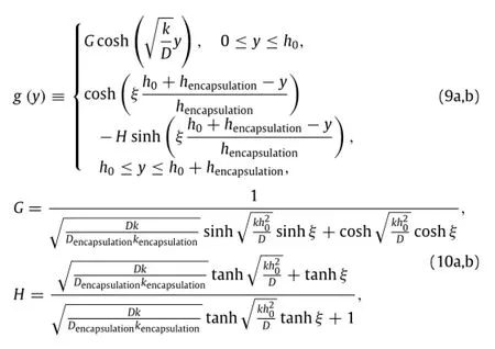
Satisfying the reactive diffusion equation,together with inhomogeneousboundarycondition,zerowaterfluxatthebottom of Mg layer,and continuity conditions,the particular solutionwpis solved aswp=w0g(y),where
In the same manner as described in the previous section,the remaining thickness h of the Mg layer normalized by its initial thickness h0is obtained as
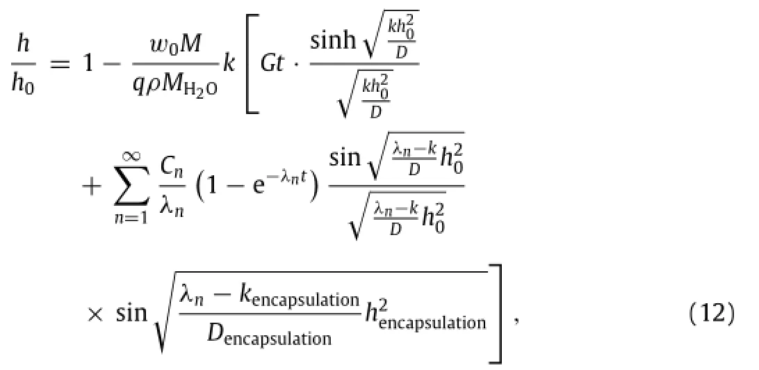
whereGisgiveninEq.(10a).AsMgisbelowtheMgOencapsulation layer,itisdifficulttomeasurethethicknesschangeofMg.Noticing MgO is not conductive,the electric resistance of Mg(or this bilayered structure)is then measured,from which the thickness can be calculated h=R0h0/R.To understand the thickness effect of MgO encapsulation,both 400 nm-thick and 800 nm-thick MgO layers are studied on a 300 nm-thick Mg layer.As shown in Fig.4(c),the normalized electrical resistance R/R0versus the normalized timepredicted from the theory agrees well with the experimental measurements.A comparison between two Mg+MgO structure layouts indicates a substantial increase in the dissolution time as the thickness of encapsulation layer increases. ThiscomesfromthefactthatthediffusionofwaterinMgOismuch slowerthanthatinMg,whicheffectivelyextendsthelifetimeofMg in providing an effective way to control the dissolution time.

The summation on the right hand side of Eq.(12)is negligible for devices relevant totransient implants.As a result,the thickness decreases linearly with time.The simple and approximate expression is given aswhere is the critical time for complete physical disappearance of the Mg conductor layer in the device and tcis the critical time in the single-layer system.From the remaining thickness h,the rate of dissolution can be solved as′.The rateofdissolutionisapproximatelylinearwiththeinitialthickness h0and it can be further simplified for a sufficiently thin Mg layer
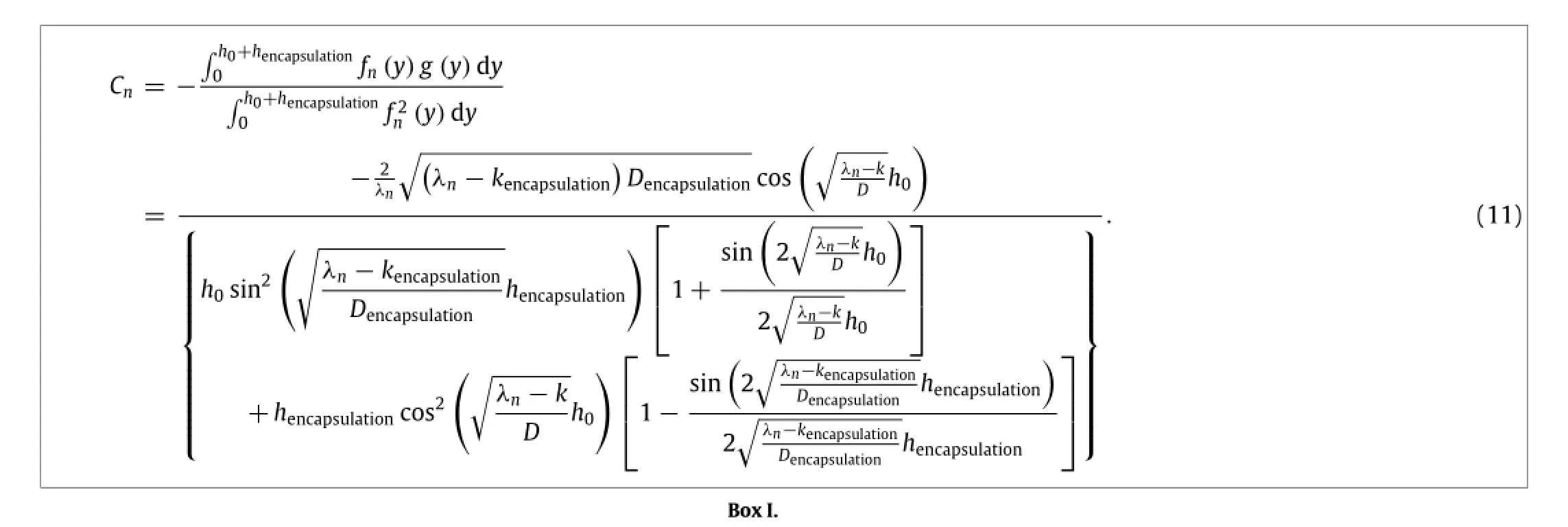
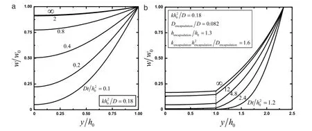
Fig.3.Distribution of water concentration predicted from models of reactive diffusion for the normalized timeand∞in(a)an Mg layerwithoutencapsulationlayer,and(b)bothanMgconductorlayerencapsulatedbyanMgOlayer
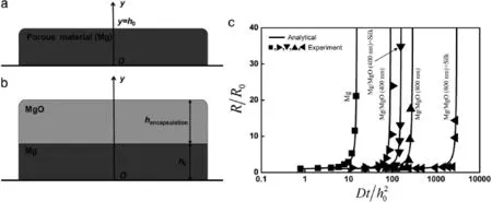
Fig.4.Schematic illustrations for models of reactive diffusion and modeling predictions of the electrical resistance compared with experimental measurements.(a)Singlelayered structure and(b)bi-layered structure used in models of reactive diffusion for porous materials.(c)Experimental and modeling results of the electric resistance of Mg and Mg with different encapsulation strategies(e.g.,MgO encapsulation layers and/or silk overcoats).
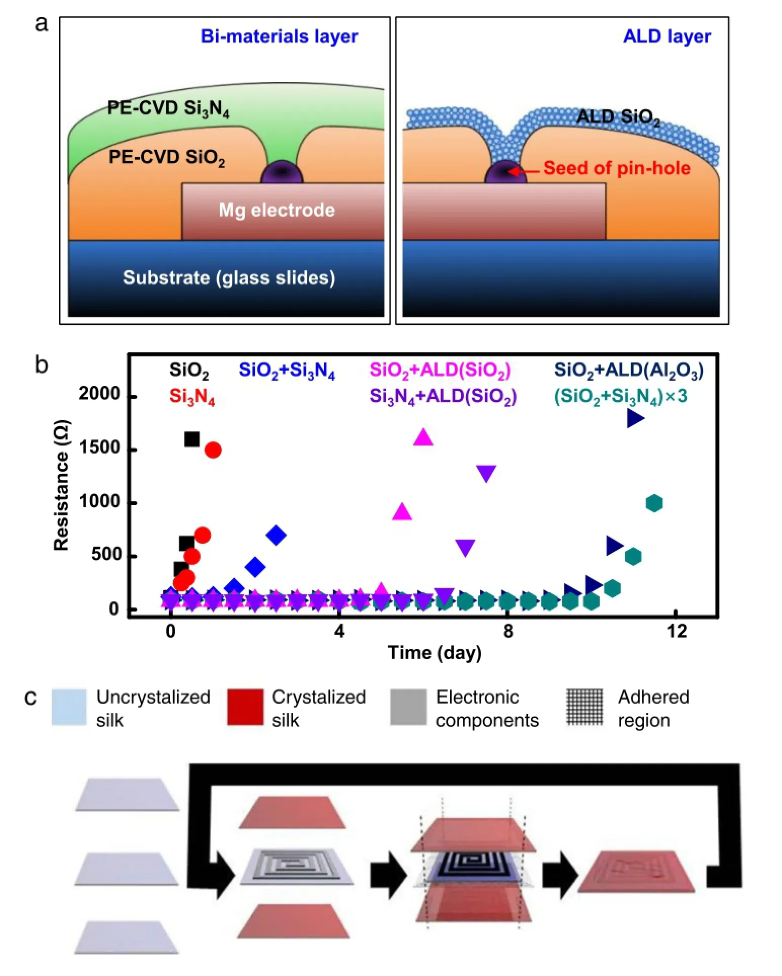
Fig.5.Encapsulation strategies with multilayer structures.(a)Schematic illustrations of encapsulation methods for transient electronic devices,with defects(e.g.,pinholes) covered by a bilayer of SiO2/Si3N4(left)or an ALD layer(right).(b)Measurements of changes in resistance of Mg traces with an initial thickness of 300 nm encapsulated with different encapsulation approaches(in deionized water at room temperature).Encapsulation strategies examined here include a single layer of PECVD SiO2(black, 1µm),PECVD-LF Si3N4(red,1µm)and ALD SiO2(orange,20 nm);a double layer of PECVD SiO2/PECVD-LF Si3N4(blue,500/500 nm),PECVD SiO2/ALD SiO2(magenta, 500/20 nm),PECVD-LF Si3N4/ALD SiO2(purple,500/20 nm);and a triple layer of PECVD SiO2/PECVD-LF Si3N4(Cyan,200/200/200/200/100/100 nm).(c)Fabrication strategy for the multilayer silk pocket.Crystallization of the outer layers renders them water insoluble,whereas the inner device substrate layer can remain crystallized.Sealing the outer edges around the device encapsulates it in a protective silk pocket.Multilayer fabrication is carried out by repeating the process with an inner pocket as the device layer.(For interpretation of the references to color in this figure legend,the reader is referred to the web version of this article.)
As an alternative,silicon oxides and nitrides can also be considered as encapsulation layers in addition to their use as gate and interlayer dielectrics,as they are typically known to be barrier materials for permeation of water[11].As a primary source of leakage for vapors or fluids,defects such as pinholes are commonly found in films of silicon oxides and nitrides.As a result,multilayer structures with different materials[11]have been developed to cooperatively eliminate defects[32]for use in transient electronics.In addition to a combination of multiple different layers,i.e.SiO2and Si3N4(Fig.5(a)left),atomic layer deposition(ALD)provides a complementary strategy to reduce defects and improve the performance of the encapsulation,even with thin layers(Fig.5(a),right)[33].As shown in Fig.5(b), measured changes in resistance of a serpentine-shaped Mg trace with an initial thickness of 300 nm demonstrate the effectiveness of several encapsulation approaches.
To achieve an even longer desired lifetime for transient electronic devices,silk overcoats have also been used to provide an extra barrier for water to diffuse into MgO and Mg layers[1]. A well designed layout with both MgO encapsulation and silk overcoat can successfully increase the lifetime of devices over hundreds of times[12].To apply the idea of multilayer structures to silk overcoats,an encapsulation strategy of exploiting multiple air pockets has been demonstrated[34].A scheme of this strategy is shown in Fig.5(c).Transient electronics transferred to a silk substrate are enclosed by silk films with tunable crystalline and diffusion properties.Thermal sealing of the silk films creates a small air pocket,which provides additional protection for the device components.Iteration of this process can provide multiple silk pockets as needed.The onset of device degradation starts only when swelling of the silk protective layer collapses the air pocket in a wet environment[35].
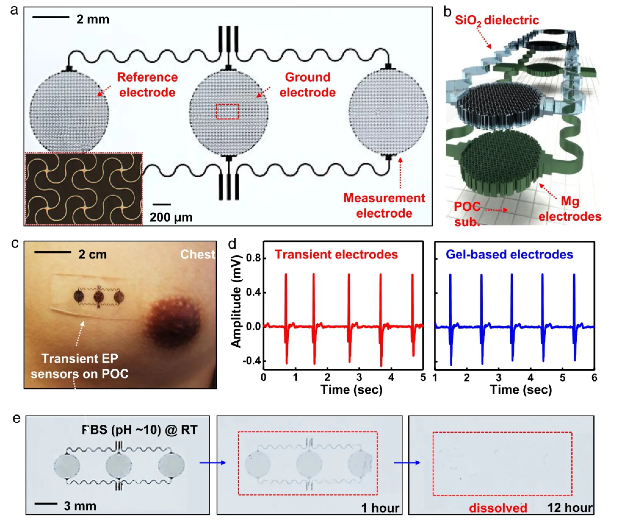
Fig.6.Transient electrophysiological sensors configured in a stretchable pattern for capacitive sensing.(a)Optical image of a device and(inset)magnified view of electrode structures in the filamentary serpentine mesh layout.(b)Schematic illustration in an exploded view for the corresponding device in(a).(c)Photograph of a device mounted onthe chestformeasurement ofelectrocardiograms(ECG).(d)ECGmeasurements collectedfrom transient(red)andstandardgel-based(blue)devices.(e)Aseries ofimages at various dissolution stages of a transient device in PBS(pH 10)at room temperature.(For interpretation of the references to color in this figure legend,the reader is referred to the web version of this article.)
These combined strategies in encapsulation lead to two-stage dissolution kinetics in transient electronics:(i)encapsulation layers define the first time period of stable operation with negligiblechangesinelectricalperformance,(ii)theMgdefinesthe second,where the device rapidly degrades.Efficient encapsulation strategies can remove the leakage pathways and significantly increase the time for stable operation.Realizing the full potential of transient electronics for implanted applications ultimately requires conformal contact with organs of the body.To this end, a recent development of transient medical devices exploits the conceptsofstretchableelectronics[36–40]byuseofbiodegradable elastomers[41].As shown in optical images and schematic illustrations(Fig.6(a)and(b)),a stretchable and transient electrophysiology sensor is constructed.Thin layers of Mg (300nm)andSiO2(100nm)aredesignedintheformoffilamentary serpentine meshes[42–44](Fig.6(a),inset)for measurement, ground and reference electrodes and connecting leads.Capacitive sensing leads to the use of a biodegradable polymer[45,46] between the Mg electrodes and the skin.The measurements show levelsoffidelitycomparabletothoseofconventionalgelelectrodes (Fig.6(d)),as demonstrated in the high quality ECG measurements on the chest(Fig.6(c)).Figure 6(e)presents a set of images of a transient electrophysiology sensor at various dissolution stages in PBS(pH 10)at room temperature.The dissolution behavior of each component is consistent with separate studies of these materials discussed in the previous section(complete dissolution within hours for Mg or days/weeks for SiO2).
5.Conclusion
When exposed to bio-fluids or water,the class of siliconbased high performance transient electronics disintegrates and dissolves to eliminate the need for recollection.A number of discoveries have been made in the effort to control how transient electronics dissolve.Firstly,a number of materials,including semiconductors,and their method of application in the design of transient electronics were studied.Secondly,a model of reactive diffusion was presented to predict the way in which a component would dissolve in bio-fluids or water.This model considered a variety of factors including the porosity of the material.Thirdly, this model was extended to study the reactive diffusion in a bilayered structure.The analytical results connect the key electricalproperty to models of reactive diffusion and provide the capability to use such analytics in conjunction with established circuit simulators as a comprehensive design approach.
Since the nature of the materials used in transient electronics exhibits a decisive effect on the dissolution of resulting electronics,future material science research would be desirable. Other strategies besides encapsulation would also be worth future research to understand multiple ways of controlling the dissolution behavior of transient electronics.Active control of the transience in devices is of interest for the future development as well. Combining possibilities in transient electronics with ideas in soft,‘tissue-like’devices further expands opportunities for applications in biomedicine.Overall,however,the research performed thus far on the design of transient electronics has been extensive and the potential use of this technology in industry is evident.
Acknowledgments
H.C.was a Howard Hughes Medical Institute International Student Research fellow.The authors acknowledge the start-up fund provided by the Engineering Science and Mechanics Department, College of Engineering,and Materials Research Institute at the Pennsylvania State University(215-37 1001 cc:H.Cheng).
References
[1]S.-W.Hwang,H.Tao,D.-H.Kim,et al.,A physically transient form of silicon electronics,Science 337(2012)1640–1644. http://www.sciencemag.org/content/337/6102/1640.
[2]S.W.Hwang,G.Park,H.Cheng,et al.,25th anniversary article:Materials for high-performance biodegradable semiconductor devices,Adv.Mater.26 (2014)1992–2000. http://onlinelibrary.wiley.com/doi/10.1002/adma.201470082/abstract.
[3]R.O.Darouiche,Treatment of infections associated with surgical implants,N. Engl.J.Med.350(2004)1422–1429. http://www.nejm.org/doi/full/10.1056/NEJMra035415.
[4]H.Tao,S.-W.Hwang,B.Marelli,et al.,Silk-based resorbable electronic devices for remotely controlled therapy and in vivo infection abatement,Proc.Natl. Acad.Sci.111(2014)17385–17389. http://www.pnas.org/content/111/49/17385.abstract.
[5]C.Dagdeviren,S.W.Hwang,Y.Su,et al.,Transient,biocompatible electronics and energy harvesters based on ZnO,Small 9(2013)3398–3404. http://onlinelibrary.wiley.com/doi/10.1002/smll.201300146/abstract.
[6]H.L.Hernandez,S.K.Kang,O.P.Lee,et al.,Triggered transience of metastable poly(phthalaldehyde)for transient electronics,Adv.Mater.26(2014) 7637–7642. http://onlinelibrary.wiley.com/doi/10.1002/adma.201403045/abstract.
[7]C.H.Lee,S.K.Kang,G.A.Salvatore,et al.,Wireless microfluidic systems for programmed,functional transformation of transient electronic devices,Adv. Funct.Mater.25(2015)5100–5106. http://onlinelibrary.wiley.com/doi/10.1002/adfm.201502192/abstract.
[8]C.W.Park,S.K.Kang,H.L.Hernandez,et al.,Thermally triggered degradation of transient electronic devices,Adv.Mater.27(2015)3783–3788. http://onlinelibrary.wiley.com/doi/10.1002/adma.201501180/abstract.
[9]X.Huang,Y.Liu,S.W.Hwang,et al.,Biodegradable materials for multilayer transient printed circuit boards,Adv.Mater.26(2014)7371–7377. http://onlinelibrary.wiley.com/doi/10.1002/adma.201403164/abstract.
[10]S.W.Hwang,S.K.Kang,X.Huang,et al.,Materials for programmed,functional transformation in transient electronic systems,Adv.Mater.27(2015)47–52. http://onlinelibrary.wiley.com/doi/10.1002/adma.201403051/abstract.
[11]S.K.Kang,S.W.Hwang,H.Cheng,et al.,Dissolution behaviors and applications of silicon oxides and nitrides in transient electronics,Adv.Funct.Mater.24 (2014)4427–4434. http://onlinelibrary.wiley.com/doi/10.1002/adfm.201304293/abstract.
[12]R.Li,H.Cheng,Y.Su,et al.,An analytical model of reactive diffusion for transient electronics,Adv.Funct.Mater.23(2013)3106–3114. http://onlinelibrary.wiley.com/doi/10.1002/adfm.201203088/abstract.
[13]C.J.Bettinger,Z.Bao,Organic thin-film transistors fabricated on resorbable biomaterial substrates,Adv.Mater.22(2010)651–655. http://onlinelibrary.wiley.com/doi/10.1002/adma.200902322/abstract.
[14]M.Irimia-Vladu,P.A.Troshin,M.Reisinger,et al.,Biocompatible and biodegradable materials for organic field-effect transistors,Adv.Funct.Mater. 20(2010)4069–4076. http://onlinelibrary.wiley.com/doi/10.1002/adfm.201001031/abstract.
[15]F.Eder,H.Klauk,M.Halik,et al.,Organic electronics on paper,Appl.Phys.Lett. 84(2004)2673–2675. http://scitation.aip.org/content/aip/journal/apl/84/14/10.1063/1.1690870.
[16]D.H.Kim,Y.S.Kim,J.Amsden,et al.,Silicon electronics on silk as a path to bioresorbable,implantable devices(vol 95,133701,2009),Appl.Phys.Lett.95 (2009). http://scitation.aip.org/content/aip/journal/apl/95/13/10.1063/1.3238552.
[17]S.-K.Kang,G.Park,K.Kim,et al.,Dissolutionchemistryandbiocompatibilityof silicon-and Germanium-based semiconductors for transient electronics,ACS Appl.Mater.Interfaces 7(2015)9297–9305. http://pubs.acs.org/doi/abs/10.1021/acsami.5b02526.
[18]J.D.Rimstidt,H.L.Barnes,The kinetics of silica–water reactions,Geochim. Cosmochim.Acta 44(1980)1683–1699. http://www.sciencedirect.com/science/article/pii/0016703780902203.
[19]H.Seidel,L.Csepregi,A.Heuberger,et al.,Anisotropic etching of crystalline silicon in Alkaline-solutions.1.Orientation dependence and behavior of passivation layers,J.Electrochem.Soc.137(1990)3612–3626. http://jes.ecsdl.org/content/137/11/3612.
[20]S.-W.Hwang,G.Park,C.Edwards,et al.,Dissolution chemistry and biocompatibility of single-crystalline silicon nanomembranes and associated materials for transient electronics,ACS Nano 8(2014)5843–5851. http://pubs.acs.org/doi/abs/10.1021/nn500847g.
[21]H.Seidel,L.Csepregi,A.Heuberger,et al.,Anisotropic etching of crystalline silicon in Alkaline-solutions.2.Influence of dopants,J.Electrochem.Soc.137 (1990)3626–3632.http://jes.ecsdl.org/content/137/11/3612.
[22]L.Yin,A.B.Farimani,K.Min,et al.,Mechanisms for hydrolysis of silicon nanomembranes as used in bioresorbable electronics,Adv.Mater.27(2015) 1857–1864. http://onlinelibrary.wiley.com/doi/10.1002/adma.201404579/abstract.
[23]P.V.Danckwerts,Absorption by simultaneous diffusion and chemical reaction,Trans.Faraday Soc.46(1950)300.http://pubs.rsc.org/en/Content/ ArticleLanding/1950/TF/TF9504600300#!divAbstract.
[24]I.A.Taub,W.Roberts,S.LaGambina,etal.,Mechanismofdihydrogenformation in the magnesium–water reaction?J.Phys.Chem.A 106(2002)8070–8078. http://pubs.acs.org/doi/abs/10.1021/jp0143847.
[25]L.Yin,H.Cheng,S.Mao,et al.,Dissolvablemetalsfor transientelectronics,Adv. Funct.Mater.24(2014)645–658. http://onlinelibrary.wiley.com/doi/10.1002/adfm.201301847/abstract.
[26]H.Inoue,K.Sugahara,A.Yamamoto,et al.,Corrosion rate of magnesium and its alloys in buffered chloride solutions,Corros.Sci.44(2002)603–610. http://www.sciencedirect.com/science/article/pii/S0010938X01000920.
[27]W.Ng,K.Chiu,F.Cheng,Effect of pH on the i in vitro/i corrosion rate of magnesium degradable implant material,Mater.Sci.Eng.C 30(2010)898–903. http://www.sciencedirect.com/science/article/pii/S0928493110000895.
[28]G.Wirth,J.Gieskes,The initial kinetics of the dissolution of vitreous silica in aqueous media,J.Colloid Interface Sci.68(1979)492–500. http://www.sciencedirect.com/science/article/pii/0021979779903072.
[29]W.G.Worley,DissolutionKineticsandMechanismsinQuartz-and Grainite-WaterSystems,MassachusettsInstituteofTechnology,1994, http://dspace.mit.edu/handle/1721.1/28068.
[30]M.Pourbaix,Atlas of Electrochemical Equilibria in Aqueous Solutions,1974.
[31]J.P.Hoare,Oxide film studies on iron in electrochemical machining electrolytes,J.Electrochem.Soc.117(1970)142–145. http://jes.ecsdl.org/content/117/1/142.abstract.
[32]J.Rosink,H.Lifka,G.Rietjens,et al.,34.1:Ultra-thin encapsulation for largearea OLED displays.Paper Presented at:SID Symposium Digest of Technical Papers,Wiley Online Library,2005. http://onlinelibrary.wiley.com/doi/10.1889/1.2036236/abstract.
[33]J.Meyer,P.Görrn,F.Bertram,et al.,Al2O3/ZrO2 nanolaminates as ultrahigh gas-diffusion barriers—A strategy for reliable encapsulation of organic electronics,Adv.Mater.21(2009)1845–1849. http://onlinelibrary.wiley.com/doi/10.1002/adma.200803440/abstract.
[34]M.A.Brenckle,H.Cheng,S.Hwang,et al.,Modulated degradation of transient electronic devices through multilayer silk fibroin pockets,ACS Appl.Mater. Interfaces(2015). http://pubs.acs.org/doi/abs/10.1021/acsami.5b06059?journalCode=aamick.
[35]B.D.Lawrence,S.Wharram,J.A.Kluge,et al.,Effect of hydration on silk film material properties,Macromol.Biosci.10(2010)393–403. http://www.ncbi.nlm.nih.gov/pubmed/20112237.
[36]H.Cheng,Y.Zhang,K.-C.Hwang,et al.,Buckling of a stiff thin film on a prestrained bi-layer substrate,Int.J.Solids Struct.51(2014)3113–3118. http://www.sciencedirect.com/science/article/pii/S002076831400198X.
[37]H.Cheng,J.Wu,M.Li,et al.,An analytical model of strain isolation for stretchable and flexible electronics,Appl.Phys.Lett.98(2011)061902. http://scitation.aip.org/content/aip/journal/apl/98/6/10.1063/1.3553020.
[38]D.-H.Kim,N.Lu,R.Ma,et al.,Epidermal electronics,Science 333(2011) 838–843.https://www.sciencemag.org/content/333/6044/838.abstract.
[39]J.A.Rogers,T.Someya,Y.G.Huang,Materials and mechanics for stretchable electronics,Science 327(2010)1603–1607. http://www.sciencemag.org/content/327/5973/1603.abstract.
[40]J.Viventi,D.H.Kim,J.D.Moss,et al.,A conformal,bio-interfaced class of silicon electronics for mapping cardiac electrophysiology,Sci.Transl.Med.2(2010) http://pubs.acs.org/doi/abs/10.1021/jp0143847.
[41]S.-W.Hwang,C.H.Lee,H.Cheng,et al.,Biodegradable elastomers and silicon nanomembranes/nanoribbons for stretchable,transient electronics, and biosensors,Nano Lett.15(2015)2801–2808. http://pubs.acs.org/doi/abs/10.1021/nl503997m.
[42]D.H.Kim,J.L.Xiao,J.Z.Song,et al.,Stretchable,curvilinear electronics based on inorganic materials,Adv.Mater.22(2010)2108–2124. http://onlinelibrary.wiley.com/doi/10.1002/adma.200902927/abstract.
[43]D.H.Kim,J.H.Ahn,W.M.Choi,et al.,Stretchable and foldable silicon integrated circuits,Science 320(2008)507–511. http://www.sciencemag.org/content/320/5875/507.
[44]R.H.Kim,M.H.Bae,D.G.Kim,et al.,Stretchable,transparent graphene interconnects for arrays of microscale inorganic light emitting diodes on rubber substrates,Nano Lett.11(2011)3381–3886. http://pubs.acs.org/doi/abs/10.1021/nl202000u.
[45]S.W.Hwang,J.K.Song,X.Huang,et al.,High-performance biodegradable/transient electronics on biodegradable polymers,Adv.Mater.26(2014) 3905–3911. http://onlinelibrary.wiley.com/doi/10.1002/adma.201306050/abstract.
[46]J.Yang,A.R.Webb,G.A.Ameer,Novel citric acid–based biodegradable elastomers for tissue engineering,Adv.Mater.16(2004)511–516. http://onlinelibrary.wiley.com/doi/10.1002/adma.200306264/abstract.
10 October 2015
http://dx.doi.org/10.1016/j.taml.2015.11.012
2095-0349/©2016 The Authors.Published by Elsevier Ltd on behalf of The Chinese Society of Theoretical and Applied Mechanics.This is an open access article under the CC BY license(http://creativecommons.org/licenses/by/4.0/).
∗.
E-mail address:huanyu.cheng@psu.edu(H.Cheng).
杂志排行
Theoretical & Applied Mechanics Letters的其它文章
- Editorial:Recent advances in mechanics of unconventional electronics
- The finite deformation of the balloon catheter
- Adhesion-governed buckling of thin-film electronics on soft tissues
- Mechanics of bioinspired imaging systems
- Recent advances on thermal analysis of stretchable electronics
- Acoustomechanics of semicrystalline polymers
