放电等离子烧结技术在陶瓷材料制备中的应用
2016-10-12冲湖北工业大学材料科学与工程学院武汉430068
熊 焰,刘 冲湖北工业大学材料科学与工程学院,武汉430068
放电等离子烧结技术在陶瓷材料制备中的应用
熊焰,刘冲
湖北工业大学材料科学与工程学院,武汉430068
放电等离子烧结 (SPS) 作为一种先进的材料制备技术,与传统烧结方法相比,在材料制备效率及所制备的材料的性能方面都有明显的提高,因而引起了世界范围的关注与深入研究。基于相关文献报道,本文针对SPS技术在陶瓷材料中应用中的若干基础问题进行了评述,分别就陶瓷SPS过程中的等离子放电现象、温度与温度场分布、电流电场的促进作用、升温制度选择与设置、压力的作用与使用、模具的设计与开发等控制参数对材料烧结行为、微观结构与宏观性能的影响进行了讨论,并简要介绍了纳米陶瓷SPS过程中微观结构自发均匀化现象。
放电等离子烧结;工艺参数;密实化机理;微观结构均匀化
上世纪90年代日本住友石炭矿业公司 (Sumitomo Coal Mining Ltd. Co., SCM,现已更名为SPS SYNTEX) 推出Dr. SINTER系列烧结炉,首次实现了放电等离子烧结 (Spark Plasma Sintering, SPS)技术的商业化。这一技术一经公开就立即引起了材料科学与工程界的极大兴趣,并首先在金属粉末冶金领域得到迅速推广。与传统的粉末冶金技术相比,SPS能够在更低的温度实现材料的快速密实化。例如,超细金属Ni粉的密实化采用传统热压 (Hot Press, HP) 烧结技术在700ºC保温150 min后,烧结体的相对密度约为95%;而采用SPS技术达到相同的密度只需要在500ºC相同压力下保温1 min[1],不仅能耗大幅降低,而且制备效率得到大幅提升。这一技术特点使得SPS在陶瓷材料领域也得到迅速发展,研究表明尤其是具有较低扩散系数的高熔点材料如氮化物[2]、硼化物[3]、碳化物[4]等都能够在SPS条件下实现相对低温下的快速制备。材料制备效率的大幅提升成为SPS技术迅速发展的重要驱动力。
SPS技术迅速发展的另一重要驱动力是所制备材料性能远优于传统方法,例如,SPS条件下Sialon陶瓷的超塑性能够达到10-2级数 (传统条件下制备的材料超塑性一般小于10-3)[5],所制备的BiTiO3陶瓷电容率高达3500 (传统方法制备的材料电容率仅为1500)[6],透明AlN陶瓷的光学性能更加良好,最大透过率大于50% (传统制备方法仅能达到约40%)[7]。
材料性能的提高与SPS独特的材料制备模式密切相关。SPS烧结设备结构如图1所示。区别于传统烧结技术的辐射加热模式,SPS利用脉冲电流通过模具及导电样品,具有更高的热效率,可以实现样品的快速加热与冷却,因此能够有效抑制升温过程晶粒的生长,保留所需的高温结构与物相成份,实现对材料微观结构的灵活调控[8]。此外,与传统HP烧结类似,SPS过程同样能够施加外部轴向压力辅助烧结过程,并且压力值更高 (目前采用石墨模具烧结压力可达到100 MPa ~ 150 MPa),能够在较低温度实现材料的快速密实化,从而降低可能的成份挥发、抑制不良相变的发生[9]。

图1 放电等离子烧结设备结构示意图Figure 1 Scheme of spark plasma sintering apparatus
自从1992年3月日本SCM公司采用SPS技术成功烧结了氧化锆-不锈钢功能梯度材料(Functional Graded Materials, FGMs)[10]以来,对SPS烧结技术的研究与应用一直在不断地深入。目前,SPS技术不仅在传统结构陶瓷材料的烧结中广泛应用[11-14],在许多先进功能材料如准晶[15]、石墨烯复合材料[16]、热电材料[17]、磁性材料[18]、生物材料[19]、透明材料[20]等合成与制备中优势突出。以日本SYNTEX、德国FCT等为代表的制备厂商相继开发出连续SPS烧结设备,SPS技术正在从实验室走向工业化大规模生产[21]。
SPS技术在材料制备效率与材料性能提升方面的巨大优势引发了各国学者对SPS技术更为深入的探索。与传统烧结方法相比,SPS提供了更加灵活的温度制度控制和更为宽泛的压力调节,脉冲电流加热的方式也为新材料的研发与制备提供了更多可能的契机。针对SPS烧结的特点,各国学者围绕SPS过程中等离子/放电现象、电流/电场对于烧结的促进作用、快速升降温速率与高压力对于材料烧结行为的影响等诸多方面开展广泛的研究,明晰SPS工艺参数-材料微观结构-材料宏观性能三者之间的相互联系。在这一过程中,不仅合成、制备出了大量的新型材料,也开发出了许多SPS的新型应用方法与使用技巧。但是,尽管如此,学界目前对于诸如SPS快速密实化机理、电场在烧结中的作用等基础问题仍未形成统一的解释。
本文将针对SPS技术在陶瓷材料应用中的若干问题进行综述讨论。
1 放电/等离子体的存在与作用
块体陶瓷材料是由陶瓷粉末烧结制备而成的,而活化烧结的方法之一就是利用电流。由于SPS技术利用低电压、大脉冲电流的加热方式,因此也被称作“脉冲电流烧结”(Pulsed Electric Current Sintering, PECS) 或“电脉冲辅助密实化”(Electric Pulse Assisted Consolidation) 技术。早在1933年,美国专利[22]中就有利用脉冲电流或放电促进金属粉体烧结的相关报道,随后在上世纪50年代到70年代美国和日本学者对“放电烧结”技术进行了大量的研究[23]。
关于SPS技术快速致密化机理的解释之一是放电与等离子体激发在烧结过程中的作用。Omori[24]在采用SPS技术烧结金属粉体时观察到烧结过程中形成的“放电颈部”及粉末颗粒间的网状“桥连”,并提出粉末颗粒微区存在电场诱导的正负极,在脉冲电流作用下颗粒间产生放电,激发等离子体,这种等离子体对颗粒表面的净化作用促进了烧结。Ishiyama等[25]认为在脉冲电流的作用下金属颗粒之间可能产生等离子体,从而对烧结过程以及取向性晶粒的形成发挥作用;同时在脉冲电场的作用下金属原子的扩散自由能降低,加速了原子的扩散,并且自身电阻加热也有利于塑性变形,因此SPS也被称为等离子活化烧结 (Plasma-Assisted Sintering, PAS)[26]。
金属材料SPS快速密实化的解释也被“借用”到非导电陶瓷材料的烧结中。一些学者将SPS技术快速密实化的机理主要归结于烧结过程中颗粒间的放电与等离子体的激发。Wang等人[27,28]通过对SPS温度场的模拟分析认为,烧结过程中最可能产生等离子体的区域是模腔中电磁场最强的区域 (即靠近压头边缘的区域),烧结时最可能产生等离子体的时间是电流变化最大的瞬间。然而,大多数陶瓷粉体并非为导电体。Tomino等人[29]的研究显示,当烧结电流为1000 A时,通过非导电Al2O3样品的电流小于100 mA;Carney等人[30]的研究也显示,脉冲电流的变化对于通过非导电样品中的电流改变并无显著贡献。Hulbert等人[31,32]采用原位原子发射显微镜测量、原位光学显微镜观测以及超快原位电压测量三种方法对SPS烧结非导电陶瓷材料的过程是否存在放电等离子进行了原位测量,均未发现SPS过程中有颗粒间的放电现象或是等离子的存在。对于非导电材料SPS过程中放电与等离子一直缺乏有力的实验佐证。目前,一般认为在非导电陶瓷材料中放电/等离子体并非材料密实化或性能提升的主要贡献因素。
2 电场的作用
如前所述,SPS过程中电流加载于上下模具压头之间使得样品处于电场条件下,因此德国FCT公司将这种烧结方式命名为“场助烧结技术”(Field Assisted Sintering Technique, FAST),并在世界范围内实现了商业化。对于电场对于SPS快速密实化中的贡献,目前仍然存在很大的争议。无可否认,电场的存在对材料内部化学结构尤其是缺陷的形成与扩散速率等方面有重要的影响作用[33]。SPS技术的知名学者Munir教授在其综述论文中提出,电场对于物质扩散的作用能够通过电子风效应,或是增加点缺陷浓度或是降低缺陷扩散激活能等方式显现[34]。Belmonet等人[35]基于SPS液相烧结Si3N4中颗粒重排与脉冲电压的相关性,提出了“电润湿”理论 (Electro-wetting theory) 的烧结机理。
对于SPS过程电场的作用,也有学者提出了不同的观点,原因是SPS过程是利用大电流、低电压进行加热 (以Dr. Sinter 1050为例,最大电流5000 A,最大电压10 V);这种模式下是否有足够的电场强度对陶瓷材料烧结产生促进作用是争论的焦点。Langer等人[36-38]将非导体Al2O3、半导体ZnO和离子导体8YSZ三种材料在150ºC/min、50 MPa的SPS条件下的烧结行为与相同压力HP条件下的烧结行为进行了实验对比,发现两者在密实化机理上并无显著差异。关于电场对于SPS烧结过程的促进作用,前期所报道的研究方法多是在实验数据基础上进行的理论计算解析[39,40],一直缺乏较为直观的实验结果。直至近期,Chen等人[41-43]在关于SPS烧结8YSZ的研究中观测到在烧结体中形成了异常的“波浪形”界面 (如图2所示),并将其归结于电场存在条件下“界面扩散为媒介的离子风”效应。
近年来,随着诸如闪烁烧结 (Flash Sintering)等新型烧结技术的出现[44,45],电场对于烧结的促进作用日益引起学者们的广泛关注。Raj等人[46]通过对模具的电路模拟指出SPS条件下能够在YSZ材料的烧结过程提供足够的电场辅助。近期,Grasso等人[47]将SPS技术与闪烁烧结技术结合,提出了“闪烁SPS” (Flash Spark Plasma Sinter, FSPS),并成功应用于纯ZrB2陶瓷的快速密实化。但是,目前对于电场在SPS过程中的贡献多是选择诸如YSZ等具有离子导体或半导体性质的材料为研究对象,对于所有陶瓷材料是否都具有类似的促进作用仍然存疑。此外,电场在SPS过程中贡献作用的多少仍然缺乏有效的量化手段进行表征。
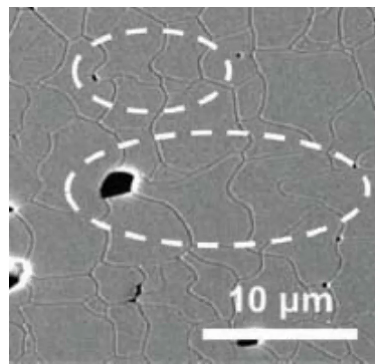
图2. SPS条件下8YSZ形成的波浪形晶界[43]Figure 2 The wave-like grain boundaries in 8YSZobtained by Chen IW et al[43]
3 温度与温度场分布
温度与温度场分布是SPS技术的一个敏感问题,模具与样品尺寸、导电性能以及模具粉料的装填等诸多因素都会对样品的实际温度场分布产生较大的影响。Vanmessnesl等人[48]通过对SPS烧结导电TiN和非导电ZrO2两种陶瓷材料的温度场进行了有限元模拟,对比结果表明:非导电ZrO2温度场由靠近模具内壁端向样品内部逐渐降低,而对于导电TiN样品温度场由样品中心向靠近模具内壁端逐渐降低;并且导电样品中存在更大的径向温度梯度。其原因可归结于电流能够直接通过导电样品,因此具有更大的热损失。Xiong等人[49]在SPS制备半透明AlN陶瓷时也发现在不添加烧结助剂的条件下很难制备大尺寸、颜色均匀的样品,其原因可归结于SPS烧结非导电陶瓷样品过程温度场分布不均匀。
因为无法在高速升温过程中对样品的实际烧结温度进行准确测量,在SPS过程中一般是借助于光学温度计或者热电偶聚焦于模具表面测量温度。对于非导电样品,考虑到石墨模具的壁厚,一般认为作用于样品的实际温度要高于测量温度。对于SPS过程中样品的实际温度,在名义烧结温度为~1600 ºC 的情况下,Suganuma等人[50]提出了如下近似计算公式:其中Ts和Tdie分别为样品计算温度和模具实际测量温度。

对于非导电样品,另一个影响温度场分布且难以控制的重要因素是接触电阻,这与样品模具装填有直接的关系[51]。实验设计如图3 (a) 所示,采用外径Φ20 mm压头与内径Φ12 mm石墨模具配合。在SPS烧结过程中温度最高的区域是石墨压头与模具接触的界面,因为其具有最大的接触电阻与电流密度;不同的接触界面 [(b) 粗糙;(c) 光滑] 会在接触面造成不同的温度梯度分布。石墨模具温度场分布虽然相对均匀,但是实际样品上下表面的温度已经产生了巨大的差异。在实际SPS过程中,由于样品置于模腔内部,接触面一般为上下压头的前端外壁与石墨模具的内壁部分;在模具装填时,需要利用碳纸调整压头与模具的间隙配合,因此保证粉料装填时上下界面的一致性是实现SPS过程温度可重复性的关键。Maizza等人[52]通过有限元法对SPS过程的温度与温度场分布进行了建模,强调模拟的准确性与接触电阻密切相关。
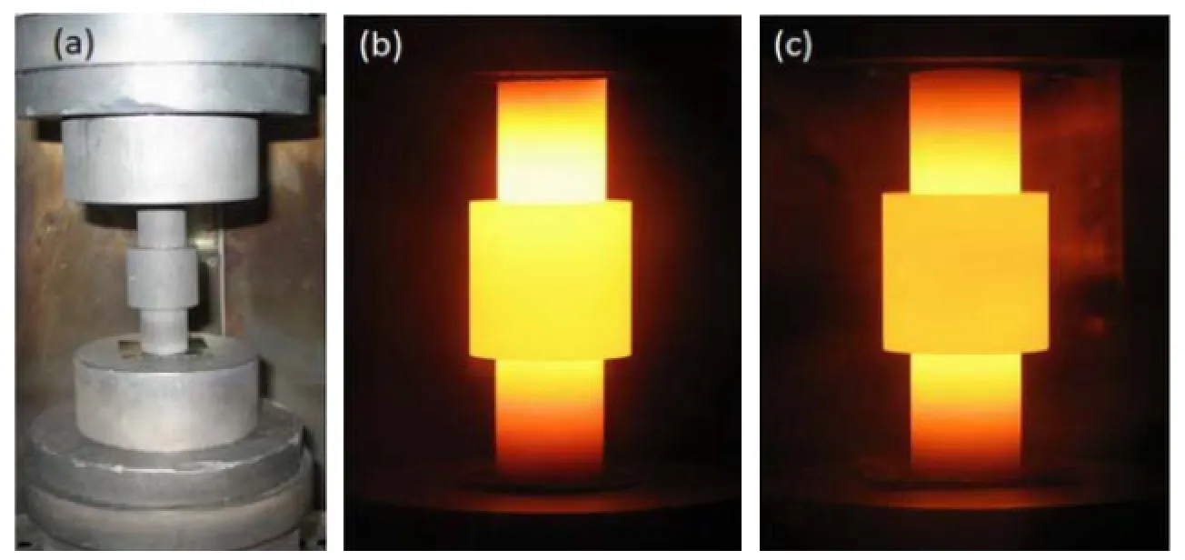
图3 模具接触面接触电阻对SPS温度场分布的影响Figure 3 Influences of surface contacting resistance on the temperature-distribution in spark plasma sintering
4 升温制度的应用
SPS设备提供了方便的升温速率控制方法,能够在较为宽泛的范围内实现升温速率调节。高速升温能够有效抑制晶粒在加热过程的生长熟化,因此在纳米陶瓷材料制备中多采用较快的升温制度。此外,高速升温能使得烧结过程远离平衡状态,不仅有利于非均质结构材料的制备,同时也丰富了烧结过程的动力学与热力学过程研究[53]。一个典型的例证便是Shen等人[54]在SPS液相烧结Si3N4陶瓷时应用“快速熟化机制”(Dynamic Ripening Mechanism),即在SPS高速升温条件下使Si3N4晶粒通过各项异性的Oswald熟化形成Si3N4长柱状互锁结构。
一些学者研究了SPS条件下升温速率与微结构的关系以及升温速率与致密化的关系,发现电流越大、升温速度越高,样品的致密化速率也越快,并且最终密实度也越高。因此,有些学者认为:要获得高密度的烧结产物,在可能的情况下应尽量提高烧结速率[55,56]。但是,日本国家材料科学研究所 (National Institution of Materials Science, NIMS) 在关于SPS制备透明Al2O3[57]、MgAl2O4[58]陶瓷的研究中却发现,较低的升温速率反而有利于得到颜色均匀、光学性能良好的烧结体,并将其原因归结于低速升温有利于晶界扩散和缺陷浓度的降低。
为了抑制烧结后期晶粒的快速生长,2000年Chen等人[59]提出了著名的“两步法烧结” (Two-Step Sintering, TSS) 技术,即首先在一个较高的温度下在烧结体中实现“冻结微观结构”,随后在较低的温度通过控制晶界迁移与晶界扩散动力学差异,实现材料的密实化同时抑制晶粒的生长。Schwarz等人[60]将这一技术应用于立方相YSZ材料的SPS过程,发现其能够有效抑制晶粒的生长,提高材料的制备效率。事实上,“两步法烧结”的概念最早是在1997年由美国加州大学伯克利分校的研究者提出的[61],他们在制备氧化铝材料的过程中通过先低温长时间保温匀化材料微观结构,再高温密实化两步工艺抑制晶粒的生长。这一概念被Chen等成功地借鉴到了SPS过程。最近,Reddy等人[62,63]又进一步提出了SPS过程的多阶段分布烧结工艺,并且应用于Al2O3和3Y-TZP纳米陶瓷的制备。
SPS设备是通过调节输出电流、电压从而调节升降温速率的,而且烧结过程中电流电压的波动相对于温度而言更为灵敏,这为更精确控制烧结制度提供了重要依据。以Ti粉和B粉在SPS中合成TiB2为例,由于反应为强放热反应,因此在温度曲线出现了瞬时的“过热”(图4),与之相伴随的是电流与电压输出的大幅降低[64]。类似的放热或者吸热反应存在于许多材料的烧结过程中,只是在一些情况下因为热量太小未能对记录曲线产生影响而在烧结过程中被忽视。但是,在某些纳米材料的烧结过程中,这种瞬时“过热”现象可能成为严重的隐患,这是因为纳米粉末的烧结活性很高,并且容易形成团聚,一点点热量就足以引起团聚体的异常长大。此时,可以通过降低升温速率,延长散热时间来防止局部过热。Shen等人[65]在制备透明纳米MgO陶瓷时,考虑到初始纳米粉体很容易吸水而形成Mg(OH)2,而Mg(OH)2在加热过程中会在450ºC左右放热还原成MgO,因此在这一温度附近采取了慢速升温或者保温的办法以防止晶粒的异常长大。

图4 SPS烧结Ti2BMg过程中电流,电源,温度与收缩位移记录[64]Figure 4 Recorded current, voltage, temperature and shrinkage versus time curves in spark plasma sintering Ti2BMg
通常情况下,SPS的升温制度是通过设定升温速率进行控制,随着温度升高电流数值逐渐增大。此外,SPS的升温制度还可以通过电流控制模式 (Current Control Mode, SPS-CCM) 进行调节,即以某一恒定电流进行升温。Sakka团队[52,66]采取CCM有限元法对SPS过程的温度及温度场的分布进行建模,并应用于超细晶WC材料的制备。近期,Niu等人[67]也利用电流控制升温模式实现了纯B4C陶瓷的超快密实化。
5 压力的作用与使用
除了加热模式的不同,SPS与传统HP技术存在诸多的相似性,因此许多学者在SPS密实化机理研究中都习惯性地与传统HP技术进行比较,一些经典的压力辅助烧结模型在SPS的研究中也得到了修正与借用。
Bernard-Granger等人[68]通过引入“应力-速率”模型研究了100 MPa压力下3Y-TZP纳米陶瓷的SPS烧结行为,指出在不同密度阶段和不同有效压力阶段,烧结行为受不同密实化机理主导。SPS过程一个典型的实验现象是密度大致处于50% ~ 90% 这一区间时极快的密实化速率,最大的密实化速率在固相烧结中能够达到10-3/s量级[69,70],在液相烧结中则可高达10-2/s量级[5]。Xu等人[71]借助于四种基于原子扩散相关过程的经典压力辅助烧结模型对3Y-TZP纳米陶瓷SPS过程早期的有效激活能进行了研究,结果表明实验所得到的数值远低于理论计算值。Langer等人[36-38]对比了三种材料的SPS烧结行为和HP烧结行为,并将材料在SPS条件下的快速密实化归结于更高的压力使用。
由于陶瓷颗粒材料的弹性模量较高,因此在传统HP技术中颗粒的塑性变形一般并不是密实化的主要机制。如前所述,SPS过程所用到的压力比传统的HP更高,Gendre等人[72,73]在碳化锆材料的SPS密实化过程中观察到晶界与晶内存在大量的位错缺陷,并提出材料的高温塑性变形是密实化的主要机制。Ji等人[74]近期也报道通过SPS技术以塑性变形为主要密实化机制制备出了B4C陶瓷。
传统HP过程一般为静态的外力载荷。Xie等人近期在国际上率先提出了振荡压力波与热场耦合烧结新技术 —— 振荡热压烧结,并且成功应用于氧化锆[75]、氮化硅[76]等材料的制备;与传统HP技术相比,振荡热压烧结在制备效率和材料性能方面优势明显。
SPS设备是通过滤波器将交流电转化为直流脉冲实现对样品的加热,以Dr. SINTER设备为例,设备优化设置的脉冲比为12:2。Salamon等人[77]通过调整设备脉冲比,在SPS过程中成功引入了振荡压力;此外还可以在SPS中通过压力输出设定,以“热锻”(Hot Forging) 方式实现材料微观结构的织构化。Zhao等[78]在SPS中对Bi2Te3进行热锻处理,有效提高了材料的热电性能与机械性能。
SPS过程压力的加载时机对材料的性能也会造成影响。一般SPS过程中,目标压力在烧结前期就完全施加在样品上。Wang等人[79]在采用SPS技术制备透明MgAl2O4时发现:随着低温阶段施加于烧结粉体的预压力提高,最终烧结体的均匀性与光学透过率都有所降低。NIMS的研究人员在透明Al2O3陶瓷的制备中也观察到了类似的实验现象,并且指出在SPS过程中采用分步加压的方式有利于高升温速率条件下提高透明Al2O3陶瓷的透光率[80]。Santanach等人[81]认为压力的分步施加更加有利于促进粉体在高温阶段的滑移与旋转。

图5 (a) 高压SPS和 (b) 无压SPS模具示意图Figure 5 Schemes of the dies used for (a) high-pressure and (b) pressureless spark plasma sintering
6 模具的设计与应用
为了制备密实的纳米晶陶瓷需要尽可能地降低烧结温度,抑制晶粒在高温下的长大。2006年Munir团队率先开发了高压SPS技术 (High Pressure Spark Plasma Sintering, HP-SPS),并且成功制备了相对密度大于98%、平均晶粒尺寸约为10 nm的氧化锆和氧化铈陶瓷[82,83]。图5 (a) 所示为HP-SPS所用模具的示意图,通过模具嵌套的方式可以将SPS过程的轴向压力提高至1 GPa。Munir等人认为高压力在烧结初期有利于颗粒的重排和打破团聚体;在烧结后期颗粒在高压力下的塑形或是超塑性变形是促进致密化的关键。由于在烧结过程中与样品的接触面采用了碳化硅 (SiC) 压头,基本阻隔了电流与烧结体的接触,样品的加热主要通过石墨外套的热传导,因此该方法更加类似于传统热压烧结,Trunec等人[84]将这种烧结方法命名为“暖压烧结”(Warm Press Sintering, WPS)。高压力下样品的烧结温度大大降低,有效抑制了晶粒的熟化生长,开辟了纳米陶瓷制备的新方法[85]。
关于无压SPS技术 (Pressureless Spark Plasma Sintering, PL-SPS) 最早的文献报道是2012年关于纳米HfB2粉体合成的一项研究工作[86]。PL-SPS技术所用模具如图5 (b) 所示,通过将传统石墨模具改造成为坩埚形态,完全阻隔外力施加与可能的等离子/电场等因素作用,充分利用SPS高速升温的特点抑制纳米粉体合成过程中的晶粒长大。Xie等人首先采用PL-SPS技术合成了纳米ZrC粉体,并成功实现了细晶ZrC密实陶瓷的低温制备[87]。
通过对模具的设计还能够实现在SPS烧结过程中对温度梯度的调控,为烧结行为差异较大的复合材料,特别是一些功能梯度材料的制备提供了便利。Hong等人[88]采用非对称锥形模具实现了ZrB2/SiC/ZrO2叠层复合材料的制备,Liu等人[89]通过SPS温度场调控实现了单一Ti/AlN原料组份制备Ti2AlN/TiN FGMs。
实验室条件下SPS所用到的模具一般为单模腔、对称圆柱体结构的石墨模具。随着SPS技术的发展与大规模工业化制造的要求,多模腔模具以及一些特殊形状模具也相继得到开发。例如,日本株式会社NJS目前已经采用叠层烧结的方式实现了大尺寸WC/Co-金刚石切割刀片的工业化生产;SPS制备的Al2O3陶瓷喷砂嘴具有更高的硬度、表面光洁度与更长的使用寿命;球面模具也已经在光学镜头的生产中得到应用 (图6)。此外,一些新型的模具材料也在SPS过程中得到应用。目前SPS模具多为石墨材质,电阻率约为15 μΩm、抗压强度100 MPa ~ 150 MPa,而添加了碳纤维的石墨压头可承压400 MPa[90]。对于较低温度的烧结过程 (不超过1000ºC),WC-Co、Mo合金、透明石英甚至是氧化铝陶瓷等材质的模具在作者的研究中也都有过尝试。
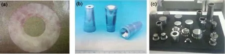
图6 (a) 150/60 mm WC/Co金刚石切割刀片;(b) 氧化铝喷砂嘴;(c) 球面模具Figure 6 (a) WC/Co diamond cutting blade and (b) Al2O3blasting nozzle by SPS. (c) Aspheric molds used in SPS.
7 SPS过程微观结构自发均匀化
SPS密实化机理一直是学术界研究的热点与难点。如前所述,SPS过程中包涵了可能的放电/等离子效应、电场促进烧结、快速升温、高辅助压力等诸多因素,多重因素的叠加作用使得对于SPS密实化机理的剖析更加复杂。尽管许多学者对以上可能影响因素分别进行了深入研究,关于SPS技术快速密实化机理至今仍然未能形成统一认识。
作者前期以3Y-TZP纳米陶瓷体系为代表,借鉴“两步法”(TSS) 原理对SPS技术密实化机理进行了探索,研究发现SPS过程能够实现陶瓷材料微观结构的自发均匀化。TSS要求在第一步烧结后微观结构发生“冻结”,并且形成相对于密实化不稳定的气孔结构,这种结构的形成一般通过密度进行标定。为进一步抑制升温过程中的晶粒生长,提高第一步烧结的密实度,作者采用SPS技术作为“两步法”烧结的第一步 (记为SPS-TSS)。研究发现当样品在第一步无压烧结后密度达到 ~83%即可通过常规的TSS实现密实化,结果与Mazaheri等人[91]采用相同初始粉体进行TSS烧结所得到的结果吻合,并确定了1100ºC为晶粒起始生长温度和1175ºC为“窗口”烧结温度。但是研究发现 (表1所示),采用SPS作为第一步烧结,虽然样品的密度达到 ~93% 且晶粒尺寸更小,但是在第二步烧结条件相同的情况下,样品的最终密度反而更低。
为了探究SPS-TSS失效原因,作者对SPS烧结密度达到 ~93% 的样品在第二步1100ºC无压烧结过程中的微观结构变化进行了表征。如图7 (a) 所示,样品在SPS烧结后晶粒尺寸细小,平均约为65 nm;气孔分布均匀,最大气孔尺寸约为50 nm。1100ºC无压烧结5 h后,平均晶粒尺寸仅为110 nm左右,晶粒生长因子约为2.0;但是烧结体中气孔出现了大尺度的异常生长,最大气孔尺寸在500 nm左右 [图7 (b)],气孔生长因子高达 ~ 10。这些大尺寸气孔无法在1100ºC无压烧结过程中去除,因此保温30 h后样品密度也只有95.4%。微观结构对比表明:SPS烧结样品中气孔尺寸细小,均匀分布于三角晶界,异常的气孔生长行为得到有效抑制,实现了“微观结构的自发均匀化”。

表1 传统两步法 (TSS) 与SPS两步法 (SPS-TSS) 烧结结果对比Table 1 Comparisons of the results of conventional TSS and SPS-TSS

图7 (a) 第一步SPS烧结 ~93% 样品与 (b) 第二步1100°C无压烧结5 h样品的微观结构照片Figure 7 SEM observations of (a) the samples with ~93% relative density obtained by the first SPS and (b) the sample after second-step pressureless sintering at 1100°C for 5 h
作者将SPS-TSS过程的失效与SPS过程微观结构的自发均匀化归结于纳米陶瓷的“增强颗粒重排”,即:有别于经典理论中“颗粒重排”的定义,纳米陶瓷烧结中颗粒重排对于烧结的贡献大幅提升,而且有效作用阶段也向高密度烧结区间大幅延伸[92]。颗粒旋转、滑移等运动行为受到颗粒尺寸、烧结颈部等因素的制约影响,而快速升温能够有效抑制晶粒与颈部的生长;高压力的辅助能够增强烧结过程中颗粒的重排运动行为。与传统烧结方法相比,纳米陶瓷的“增强颗粒重排”行为能够在SPS过程中得到更加充分的利用。利用SPS过程微观结构的自发均匀化机理,作者成功实现透明3Y-ZTP纳米陶瓷的制备[70,93]与细晶ZrC陶瓷的低温制备[87]。近期,作者利用高压SPS模具与无压SPS模具设计,分别讨论了SPS过程中电场、压力、升温速率等因素对于SPS过程微观结构自发均匀化的贡献。研究发现:辅助压力是实现SPS纳米陶瓷烧结微观结构的自发均匀化的关键因素,可能的电场、高速升温等参数对于SPS微观结构的自发均匀化并无决定性的影响[94]。这一结果可能有助于非导体陶瓷材料SPS快速密实化机理的解释。
8 结束语
从第一台商业化烧结装置问世至今,SPS技术经历了二十多年的发展。随着烧结装备、烧结方法、使用技巧的不断升级创新,SPS技术在陶瓷材料微观结构与宏观性能调控、结构-功能一体化陶瓷材料设计、先进多功能陶瓷制备等诸多方面显示出了越来越广阔的应用前景。随着研究的不断深入,诸如电场对于SPS过程的促进作用、非导体陶瓷材料的密实化机理等诸多基础科学问题解释也将逐渐明晰。尽管每年发表的相关学术论文中中国学者的工作占据了一半以上,但是我国在SPS装备制造、SPS技术在工业领域的应用推广等诸多方面仍然相对滞后。目前我国经济结构正在面临转型升级,相关领域节能降耗减排的环保要求不断提升,为SPS技术基础科学研究和大规模制造业的推广提供了良好的发展契机。
致 谢
感谢季伟博士对于文献整理、项铭禹博士对于文稿校正所提供的帮助。
[1] GUBICZA J, BUI HQ, FELLAH F, et al. Microstructure and mechanical behaviour of ultrafine-grained Ni processed by different powder metallurgy methods [J]. Journal of Materials Research, 2009, 24: 217-226.
[2] LEE JW, MUNIR ZA, SHIBUYA M. Synthesis of dense TiB2-TiN nanocrystalline composites through mechanical and field activation [J]. Journal of the American Ceramic Society, 2001, 84: 1209-1216.
[3] RISBUD SH, GROZA JR, KIM MJ. Clean grain boundaries in aluminium nitride ceramics densified without additives by a plasma-activated sintering process [J]. Philosophical Magazine, 1994, 63: 525-533.[4] OHYANAGI M, YAMAMOTO T, KITAURA H, et al. Consolidation of nanostructured β-SiC with disorder-order transformation [J]. Scripta Materialia, 2004, 50: 111-114.
[5] SHEN ZJ, PENG H, NYGREN M. Formidable increase in the superplasticity of ceramics in the presence of an electric field [J]. Advanced Materials, 2003, 15: 1006-1009.
[6] TAKEUCHI T, BETOURNE E, TAUCHI M et al. Dielectric properties of spark-plasma-sintered BaTiO3[J]. Journal of Materials Science, 1999, 34: 917-924.
[7] XIONG Y, FU ZY, WANG H, et al. Microstructure and IR transmittance of spark plasma sintering translucent AlN ceramics with CaF2additive. Materials Science and Engineering B, 2005, 123: 57-62.
[8] NYGEN M, SHEN ZJ. On the preparation of bio-, nano- and structural ceramics and composites by spark plasma sintering [J]. Solid State Science, 2003, 5: 125-131.
[9] CHEN XJ, KHOR KA, CHAN SH, et al. Overcoming the effect of contaminant in solid oxide fuel cell(SOFC) electrolyte: Spark plasma sintering (SPS) of 0.5 wt.% silica-doped yttria-stabilized zirconia (YSZ)[J]. Materials Science and Engineering A, 2004, 374 (1-2): 64-71.
[10] TOKITA M. Trends in advanced spark plasma sintering systems and technology [J]. Journal of the Society of Powder Technology, Japan, 1993, 30: 790-804.
[11] NYGEN M, SHEN ZJ. Spark plasma sintering: Possibilities and limitations [J]. Key Engineering Materials,2004, 264-268: 719-724.
[12] ORRU R, LICHERI R, LOCCI AM, et al. Consolidation/synthesis of materials by electric activated/assisted sintering [J]. Materials Science and Engineering R, 2009, 63: 127-287.
[13] MUNIR ZA, QUACH DV, OHYANAGI M. Electric current activation of sintering: A review of the pulsed electric current sintering process [J]. Journal of the American Ceramic Society, 2011, 94: 1-19.
[14] OLEVSKY EA, BRADBURY WL, HAINES CD, et al. Fundamental aspects of spark plasma sintering: I. Experimental analysis of scalability [J]. Journal of the American Ceramic Society, 2012, 95: 2406-2413.
[15] RAMOND L, BERNARD-GRANGER G, Addad A, et al. Sintering of a quasi-crystalline powder using spark plasma sintering and hot-pressing [J]. Acta Materialia, 2010, 58: 5120-5128.
[16] WALKER LS, MAROTTO VR, RAFIEE MA, et al. Toughening in grapheme ceramic composites [J]. ACS Nano, 2011, 5: 3182-3190.
[17] CHEN ZG, HAN G, YANG L, et al. Nanostructured thermoelectric materials: Current research and future challenge [J]. Progress in Natural Science: Materials International, 2012, 22: 535-549.
[18] GARAY JE. Current-activated, pressure-assisted densification of materials [J]. Annual Review of Materials Research, 2010, 40: 445-468.
[19] DROUET C, LARGEOT C, RAIMBEAUX G, et al. Bioceramics: Spark plasma sintering (SPS) of calcium phosphate [J]. Advanced Science and Technology, 2006, 49: 45-50.
[20] WANG L, JIANG W. CHEN L, et al. Formation of a unique glass by spark plasma sintering of a zeolite [J]. Journal of Materials Research, 2009, 24: 3241-3245.
[21] TOKITA M. Development of advanced spark plasma sintering (SPS) systems and its industrial applications [J]. Ceramic Transactions, 2006, 194: 51-59.
[22] TAYLOE GF. Apparatus for making hard metal compositions; 美国,US1896854 [P]. 1933-02-07.
[23] GRASSO S, SAKKA Y, MAIZZA G. Electric current activated/assisted sintering (ECAS): A review of patents 1906-2008 [J]. Science and Technology of Advanced Materials, 2009, 10: 053001.
[24] OMORI M. Sintering, consolidation, reaction and crystal growth by the spark plasma system (SPS) [J]. Materials Science and Engineering A, 2000, 287: 183-188.
[25] ISHIYAMA M. Plasma activated sintering (PAS) system [J]. Journal of the Japan Society of Powder and Powder Metallurgy, 1993, 40: 931-934
[26] SHON IJ, MUNIR A. Synthesis of MoSi2-xNb and MoSi2-yZrO2composites by the field-activated combustion method [J]. Materials Science and Engineering A, 1995, 202: 256-261.
[27] WANG YC, FU ZY. Study of temperature field in spark plasma sintering [J]. Materials Science and Engineering B, 2002, 90: 34-37.
[28] WANG YC, FU ZY. Study of temperature field in spark plasma sintering BN [J]. Journal of Wuhan University of Technology (Materials Science Edition), 2002, 17: 1-4.
[29] TOMINO H, WATANABE H, KONDO Y. Electric current path and temperature distribution for spark sintering [J]. Journal of the Japan Society of Powder and Powder Metallurgy, 1997, 44: 974-979.
[30] CARNEY CM, MAH TI. Spark plasma sintering of conductive and nonconductive ceramics [J]. Journal of the American Ceramic Society, 2008, 91: 3448-3450.
[31] HULBER DM, ANDERS A, DUDINA DV, et al. The absence of plasma in spark plasma sintering [J]. Journal of Applied Physics, 2008, 1040: 033305.
[32] HULBER DM, ANDERS A, DUDINA DV, et al. A discussion on the absence of plasma in spark plasma sintering [J]. Scripta Materialia, 2009, 60: 835-838.
[33] RAJ R, COLOGNA M, and FRANCIS JSC. Influence of externally imposed and internally generated electrical fields on grain growth, diffusional creep, sintering and related phenomena in ceramics [J]. Journal of the American Ceramic Society, 2011, 94: 1941-1965.
[34] MUNIR ZA, ANSELMI-TAMBURINI U, OHYANAGI M. The effect of electric field and pressure on the synthesis and consolidation of materials: A review of the spark plasma sintering method [J]. Journal of Materials Science, 2006, 41: 763-777.
[35] BELMONTE M, OSENDI MI, MIRANZO P. Modelling the effect of pulsing on the spark plasma sintering of silicon nitride materials [J]. Scripta Materialia, 2011, 65: 273-276.
[36] LANGER J, HOFFMANN MJ, GUILLON O. Direct comparison between hot pressing and electric field-assisted sintering of submicron alumina [J]. Acta Materialia, 2009, 57: 5454-5465.
[37] LANGER J, HOFFMANN MJ, GUILLON O. Electric field-assisted sintering and hot pressing of yttria-stabilized zirconia [J]. Journal of the American Ceramic Society, 2011, 94: 24-31.
[38] LANGER J, HOFFMANN MJ, GUILLON O. Electric field-assisted sintering and hot pressing of semiconductive zinc oxide: A comparative study [J]. Journal of the American Ceramic Society, 2011, 94: 2344-2353.
[39] GRANGER-BERNARD G, GUIZARD C. Spark plasma sintering of a commercially available granulated zirconia powder: I. Sintering path and hypotheses about the mechanism(s) controlling densification [J]. Acta Materialia, 2007, 55: 3493-3504.
[40] CHIAM R. Densification mechanisms in spark plasma sintering of nanocrystalline ceramics Materials Science and Engineering A, 2007, 443: 25-32.
[41] KIM SW, KIM SG, JUNG JI, et al. Enhanced grain boundary mobility in yttria-stabilized cubic zirconis under an electric current [J]. Journal of the American Ceramic Society, 2011, 94: 4231-4238.
[42] CHEN IW, KIM SW, LI J, et al. Ionomigration of neutral phases in ionic conductor [J]. Advanced EnergyMaterials, 2012, 2: 1383-1389.
[43] KIM SE, KANG SJL, CHEN IW. Ionomigration of pores and gas bubbles in yttria-stabilized cubic zirconina [J]. Journal of the American Ceramic Society, 2013, 96: 1090-1098.
[44] COLOGNA M, RASHKOVA B, RAJ RISHI. Flash sintering of nanograin zirconia in <5 s at 850 ºC [J]. Journal of the American Ceramic Society, 2010, 93: 3556-3559.
[45] NARAYAN J. A new mechanism for field-assisted processing and flash sintering of materials [J]. Scripta Materialia, 2013, 69: 107-111.
[46] RAJ R, REHMAN A. Can die configuration influence field-assisted sintering of oxides in the SPS process[J]. Journal of the American Ceramic Society, 2013, 96: 3697-3700.
[47] GRASSO S, SAUNDERS T PORWAL H, et al. Flash spark plasma sintering (FSPS) of Pure ZrB2[J]. Journal of the American Ceramic Society, 2014, 97: 2405-2408.
[48] VANMEENSEL K, LAPTEV A, HENNICKE J, et al. Modelling of the temperature distribution during field assisted sintering [J]. Scripta Materialia, 2005, 53: 4379-4388.
[49] XIONG Y, FU ZY, WANG H, et al. Microstructure and IR transmittance of spark plasma sintering translucent AlN ceramics with CaF2additive [J]. Materials Science and Engineering B, 2005, 123: 57-62.
[50] SUGANUMA M. KITAGAWA Y, WADA S, et al. Pulsed electric current sintering of silicon nitride [J]. Journal of the American Ceramic Society, 2003, 86: 387-394.
[51] 熊焰. SPS过程中陶瓷的微观结构控制与性能优化 [D]. 武汉: 武汉理工大学博士学位论文, 2009.
[52] MAIZZA G, GRASSO S, SAKKA, Y. Moving finite-element mesh model for aiding spark plasma sintering in current control mode of pure ultrafine WC powder [J]. Journal of Materials Science, 2009, 44: 1219-1236.
[53] SHEN ZJ, NYGRE M. Microstructural prototyping of ceramics by kinetic engineering: Applications of spark plasma sintering [J]. The Chemical Record, 2005, 5: 173-184.
[54] SHEN ZJ, ZHAO Z, PENG H, et al. Formation of tough interlocking microstructure in silicon nitride ceramics by dynamic ripening [J]. Nature, 417: 266-269.
[55] MISHRA RS, MUKHERJEE AK. Electric pulse assisted rapid consolidation of ultrafine grained alumina matrix composites [J]. Materials Science and Engineering A, 2000, 287: 178-182.
[56] LEON AB, MORIKAWA Y, KAWAHARA M, et al. Fracture toughness of nanocrystalline tetragonal zirconia with low yttria content [J]. Acta Materialia, 2002, 50: 4555-4562.
[57] KIM BN, HIRAGA K, MORITA K, et al. Effects of heating rate on microstructure and transparency of spark-plasma-sintered alumina [J]. Journal of European Ceramic Society, 2009, 29: 323-327.
[58] MORITA K, KIN BN, HIRAGA K, et al. Fabrication of transparent MgAl2O4spinel polycrystal by spark plasma sintering process [J]. Scripta Materialia, 2008, 58: 1114-1117.
[59] CHEN YI WANG XH. Sintering dense nanocrystalline ceramics without final-stage grain growth [J]. Nature, 2000, 404: 168-171.
[60] SCHWARZ S, GUILLON O. Two step sintering of cubic yttria stabilized zirconia using field-assisted sintering technique/spark plasma sintering [J]. Journal of European Ceramic Society, 2013, 33: 637-641.
[61] LIN FJT, DE JONGHE LC, RAHAMAN MN. Microstructure refinement of sintered alumina by a two-step sintering technique [J]. Journal of the American Ceramic Society, 1997, 80: 2269-2279.
[62] REDDY K M, KUMAR N, BASU B. Innovative multi-stage spark plasma sintering to obtain strong and tough ultrafine-grained ceramics [J]. Scripta Materialia, 2010, 62: 435-438.
[63] REDDY K M, KUMAR N, BASU B. Inhibition of grain growth during the final stage of multi-stage spark plasma sintering of oxide ceramics [J]. Scripta Materialia, 2010, 63: 585-588.
[64] SALAMON D, ERIKSSON M, NYGREN M, et al. Homogeneous TiB2ceramics achieved by electric current-assisted self-propagating reaction sintering [J]. Journal of the American Ceramic Society, 2007, 90: 3303-3306.
[65] CHAIM R, SHEN ZJ, NYGREN M. Transparent nanocrystalline MgO by rapid and low-temperature spark plasma sintering [J]. Journal of Materials Research, 2004, 19: 2527-2531.
[66] GRASSO S, SAKKA Y, MAIZZA G, et al. Pressure effect on the homogeneity of spark plasma sintered tungsten carbide powder [J]. Journal of the American Ceramic Society, 2009, 92: 2418-2421.
[67] NIU B, ZHANG F, ZHANG JY, et al. Ultra-fast densification of boron carbide by flash spark plasma sintering [J]. Scripta Materialia, 2016, 1163: 127-130.
[68] BERNARD-GRANGER G, ADDAD A, FANTOZZI G, et al. Spark plasma sintering of a commercially available granulated zirconia powder: Comparison with hot-pressing [J]. Acta Materialia, 2010, 58: 3390-3399.
[69] SHEN ZJ, JOHNSSON M, ZHAO Z, et al. Spark plasma sintering of alumina [J]. Journal of the American Ceramic Society, 2002, 85: 1921-1927.
[70] WANG L, POUCHLY V, MACA K, et al. Intensive particle rearrangement in the early stage of spark plasma sintering process [J]. Journal of Asian Ceramic Societies, 2015, 3:183-187.
[71] XU J, CASOLCO SR, GARAY JE. Effect of varying displacement rates on the densification of nanostructured zirconia by current activation [J]. Journal of the American Ceramic Society, 2009, 92: 1506-1513.
[72] GENDRE M, MAITRE A, TROLLIARD G. Synthesis of zirconium oxycarbide (ZrCxOy) powder: Influence of stoichiometry on densification kinetics during spark plasma sintering and on mechanical properties [J]. Journal of European Ceramic Society, 2011, 31:2377-2385.
[73] ANTOU G, PRADEILLES N, GENDRE M, et al. New approach of the evolution of densification mechanisms during spark plasma sintering: Application to zirconium (oxy-)carbide ceramics [J]. Scripta Materialia, 2015, 101: 103-106.
[74] JI W, REHMAN SS, WANG, WM, et al. Sintering boron carbide ceramics without grain growth by plastic deformation as the dominant densification mechanism [J]. Scientific Reports, 215, 5: 15827.
[75] XIE ZP, LI S, AN LN. A novel oscillatory pressure-assisted pressing for preparation of high-performance ceramics [J]. Journal of the American Ceramic Society, 2014, 97: 1012-1015.
[76] LI S, XIE ZP, XUE WJ, et al. Sintering of High-performance silicon nitride ceramics under vibratory pressure [J]. Journal of the American Ceramic Society, 2015, 98: 698-701.
[77] SALAMON D, ERIKSSON M, NYGREN M, et al. Can the use of pulsed direct current induce oscillation in the applied pressure during spark plasma sintering [J]. Science and Technology of Advanced Materials,2012, 13: 015005.
[78] ZHAO LD ZHANG BP LI JF, et al. Enhanced thermoelectric and mechanical properties in textured n-type Bi2Te3prepared by spark plasma sintering [J]. Solid State Sciences, 2008, 10: 651-658.
[79] WANG C, ZHAO Z. Transparent MgAl2O4ceramic produced by spark plasma sintering [J]. Scripta Materialia, 2009, 61: 193-196.
[80] GRASSO S, HU CF, MAIZZA G, et al. Effects of pressure application method on transparency of spark plasma sintered alumina [J]. Journal of the American Ceramic Society, 2011, 94: 1405-1409.
[81] SANTANACH JG, WEIBEL A ESTOURNES C, et al. Spark plasma sintering of alumina: Study of parameters, formal sintering analysis and hypotheses on the mechanism(s) involved in densification and grain growth [J]. Acta Materialia, 2011, 59: 1400-1408.
[82] ANSELMI-TAMBURINI U, GARAY JE, MUNIR ZA. Fast low-temperature consolidation of bulk nanometric ceramic materials [J]. Scripta Materialia, 2006, 54: 823-828.
[83] ANSELMI-TAMBURINI U, WOOLMAN JN, MUNIR ZA. Transparent nanometric cubic and tetragonal zirconia obtained by high-pressure pulsed electric current sintering [J]. Advanced Functional Materials,2007, 17: 3267-3273.
[84] TRUNEC M, MACA K, SHEN ZJ. Warm pressing of zirconia nanoparticles by the spark plasma sintering technique [J]. Scripta Materialia, 2008, 59: 23-26.
[85] MAGLIA F, TREDICI IG, ANSELMI-TAMBURINI U. Densification and properties of bulk nanocrystalline functional ceramics with grain size below 50 nm [J]. Journal of European Ceramic Society,2013, 33: 1045-1066.
[86] WANG HL, LEE SH KIM HD. Nano-hafnium diboride powder synthesized using a spark plasma sintering apparatus [J]. Journal of the American Ceramic Society, 2012, 95: 1493-1496.
[87] XIE JJ, FU ZY, WANG YC, et al. Synthesis of nanosized zirconia carbide powders by a combinational method of sol-gel and pulse current heating [J]. Journal of European Ceramic Society, 2014, 34: 13.e1-13.e 7.
[88] HONG CQ, ZHANG XH, LI WJ, et al. A novel functional graded material in the ZrB2-SiC and ZrO2system by spark plasma sintering [J]. Material Science and Engineering A, 2008, 498: 437-441.
[89] LIU Y, JIN ZH. Electric current assisted sintering of continuous functionally graded Ti2AlN/Tin Material[J]. Ceramics International, 2012, 38: 217-222.
[90] GRASSO S, YOSHIDA H, PROWAL H, et al. Highly transparent α-alumina obtained by low cost high pressure SPS [J]. Ceramics International, 2013, 39: 3243-3248.
[91] MAZAHERI M, SIMCHI A, FOLESTANI-FARD F. Densification and grain growth of nanocrystalline 3Y-TZP during two-step sintering [J]. Journal of European Ceramic Society, 2008, 28: 2933-2939.
[92] XIONG Y, HU JF, SHEN ZJ. Dynamic pore coalescence in nanoceramic consolidated by two-step sintering procedure [J]. Journal of European Ceramic Society, 2013, 33: 2087-2092.
[93] XIONG Y, FU ZY, POUCHLY V, et al. Preparation of transparent 3Y-TZP nanoceramics with no low-temperature degradation [J]. Journal of the American Ceramic Society, 2014, 97: 1402-120.
[94] LIU C, XIANG MY, FU ZY, et al. Microstructural refinement in spark plasma sintering 3Y-TZP nanoceramics [J]. Journal of European Ceramic Society, 2016, 36: 2565-2571.
State of Art: Applications of Spark Plasma Sintering Technique in Ceramic Fabrications
XIONG Yan, LIU Chong
Department of Materials Science and Engineering, Hubei University of Technology, Wuhan 430068
The advanced spark plasma sintering (SPS) technique has attracted worldwide attentions and extensive investigations due to the formidable enhancement in the material properties as well as the fabrication efficiency compared with those counterparts by conventional sintering methods. Based on the reported observations in literatures, this review focuses on the fundamental aspects of the applications of SPS technique in ceramic materials. The correlations of sintering behaviors, microstructural development and final properties are discussed by identifying the intrinsic benefits from spark plasma, electric field, temperature and temperature distribution, heating regimes,application of external force and developing of mold design. The phenomena of spontaneous microstructural refinement in spark plasma sintering nanocermics are briefly introduced as well.
Spark plasma sintering (SPS); Processing parameters; Densification mechanism;Microstructural refinement
TB321
1005-1198 (2016) 04-0227-14
A
10.16253/j.cnki.37-1226/tq.2016.04.003
及
熊焰,男,汉族,硕士生导师,美国陶瓷学会会员。2009年6月毕业于武汉理工大学材料加工工程专业,获工学博士学位。2009年8月至2011年11月,赴瑞典斯德哥尔摩大学Arrhenius实验室进行博士后研究工作。现为湖北工业大学副教授。入选湖北省新世纪高层次人才工程第三层次,湖北省“楚天学者”人才计划“楚天学子”层次。研究特长与方向:先进材料制备技术、无机非金属材料、纳米材料、生物材料。目前主持国家自然科学基金、湖北省自然科学基金等多项研究项目,共发表三大索引论文30余篇,总引用160余次。

2016-04-19
2016-05-08
国家自然科学基金 (No. 51402097)。
熊 焰 (1980 -), 男, 湖北孝感人, 副教授。E-mail: xiongyan1980@hotmail.com。