Fabrication of nanoscale speckle using broad ion beam milling on polymers for deformation analysisQinghua Wanga,∗,Satoshi Kishimotob,Yoshihisa Tanakab,Kimiyoshi Naitob
2016-09-21ReserchInstituteforMesurementndAnlyticlInstrumenttionNtionlInstituteofAdvncedIndustrilSciencendTechnologyUmezonoTsukuIrki3058568JpnNtionlInstituteforMterilsScienceSengenTsukuIrki3050047Jpn
Reserch Institute for Mesurement nd Anlyticl Instrumenttion,Ntionl Institute of Advnced Industril Science nd Technology,1-1-1 Umezono,Tsuku,Irki 305-8568,JpnNtionl Institute for Mterils Science,1-2-1 Sengen,Tsuku,Irki 305-0047,Jpn
Letter
Fabrication of nanoscale speckle using broad ion beam milling on polymers for deformation analysis
Qinghua Wanga,∗,Satoshi Kishimotob,Yoshihisa Tanakab,Kimiyoshi Naitob
aResearch Institute for Measurement and Analytical Instrumentation,National Institute of Advanced Industrial Science and Technology,1-1-1 Umezono,Tsukuba,Ibaraki 305-8568,Japan
bNational Institute for Materials Science,1-2-1 Sengen,Tsukuba,Ibaraki 305-0047,Japan
H I G H L I G H T S
·A fabrication technique of nanoscale speckle using broad ion milling was proposed.
·It is simple and low-cost to fabricate nanoscale speckle on polymers in a large area.
·Speckle morphologies under different milling times and tilt angles on different polymers were studied.
·The fabricated speckle with good time stability is useful for deformation measurement.
A R T I C L EI N F O
Article history:
in revised form
12 July 2016
Accepted 12 July 2016
Available online 21 July 2016
Nanoscale speckle
Ion beam milling
Polymer
Deformation
Digital image correlation
We first report a fabrication technique of nanoscale speckle patterns on polymers using broad ion beam milling.The proposed technique is simple and low-cost to produce speckles ranging from dozens of nanometers to less than three micrometers in a large area of several millimeters.Random patterns were successfully produced with an argon(Ar)ion beam on the surfaces of four kinds of polymers:the epoxy matrix of carbon fiber reinforced plastic,polyester,polyvinyl formal-acetal,and polyimide.The speckle morphologies slightly vary with different polymers.The fabricated speckle patterns have good time stabilityandarepromisingtobeusedtomeasurethenanoscaledeformationsofpolymersusingthedigital image correlation method.
©2016 The Authors.Published by Elsevier Ltd on behalf of The Chinese Society of Theoretical and
Applied Mechanics.This is an open access article under the CC BY-NC-ND license(http://creativecommons.org/licenses/by-nc-nd/4.0/).
Polymers,which are extensively used as substrates or matrixes in flexible electronics,aerospace materials and so on,play an essential and ubiquitous role in daily life.Micro/nano-scale deformation measurement has become a key issue for understanding the fundamental mechanical properties of polymer materials[1,2].One of the most popular methods for deformation measurement is the digital image correlation(DIC)method[3-6].With the combination of a scanning electron microscope(SEM),the DIC methodcanrealizemeasuringmicro/nano-scaledeformation[7,8]. Considerable attention has concentrated on the SEM-DIC method because of its high spatial resolution,high displacement sensitivity,noncontact and full-field properties[9,10].In the implementation process of the SEM-DIC method,fabrication of high-quality micro/nano-scale speckle or random patterns as the deformation carriers is of vital importance[11].
Common micro/nano-scale speckle fabrication techniques include electron beam lithography(EBL)[12]and focused ion beam(FIB)milling[13,14].An improved EBL technique was reported to generate a high quality micro/nano-scale random speckle pattern on various specimens[15].The FIB milling technique was often used to produce micro/nano-scale random or periodic patterns for local stress and residual stress measurement[16-19].However, due to the disadvantage of time consumption,the EBL and the FIB milling techniques can only produce micro/nano-scale speckle in a very small region and it is troublesome to splice some speckle patterns in a large area of several millimeters.Another method is using a fine point airbrush to generate random speckle patterns for micro/nano-scale deformation measurement of surface and internal planes via the DIC method[20].Nevertheless,there are some disadvantages about this method including long preparation time and complex experiment steps.Besides,chemical vapor exposure and ultraviolet(UV)lithography were also successfully utilized tofabricate random patterns[21].However,the high cost for chemical vapor exposure and the greater speckle size(2-20µm)for UV photo-lithography become the limitations for their wide applications in nanoscale measurement field.Although small-scale speckle can also be fabricated by mixing graphite powder particles and epoxy resin[22],this method is difficult to be used for nanoscale deformation due to the effect of epoxy resin and the micro speckle size(greater than 3µm).
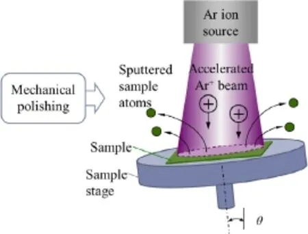
Fig.1.Schematicmapoffabricatingspecklepatternsusingbroadionbeammilling.
Broad ion beam (BIB)milling is another kind of ion beam lithography using low-energy noble gas ion beams(such as argon(Ar)Ar+and helium(He)He+).The BIB milling technique has been widely used for milling a re-shining a sample for transmission electron microscope(TEM)observation[23,24].In this study,we will put forward a new technique using BIB milling for fabricating nano-scale speckle patterns on polymer substrates in a large area withadiameterofaround10mm.Theinfluencingfactorsincluding the tilt angle and the milling time will be investigated and the verification experiments for the deformation measurement will be performed.The proposed method is believed to be easy to operate and the cost is much lower.
Four different kinds of polymer materials were chosen as the samples,on which nanoscale speckle patterns will be fabricated. These polymers have often been used in industrial and scientific fields,and their deformation characteristics are key influencing factors of their applications.
The first sample is a polyacrylonitrile(PAN)-based IM600 carbon fiber reinforced plastic(CFRP)prepreg material QC133-149A from Toho Tenax Co.,Ltd.The epoxy matrix(133)contains three-dimensional cross-linked structures formed by the reaction betweentheepoxyresinandthehardeners.CFRPisusuallyapplied in sailboats,rowing shells,modern bicycles,and motorcycles owing to its high strength-to-weight ratio and good rigidity.
The second sample includes 90%polyvinyl formal-acetal and 10%epoxy novolac.Since this polymer is widely used in flexible electronic devices such as strain gages,the deformation measurement of this kind of material has become a focus of attention in the field of flexible electronics.
The third sample is a plastic film with component of polyester in the structure of strain gages from Kyowa Electronic Instruments Co.,Ltd.Besides strain gages,the wide application of polyester also lies in making bottles,films,tarpaulin,liquid crystal displays, filters,dielectric film for capacitors,film insulation for wire and insulating tapes.
The last sample is polyimide(PI).Due to lightweight and flexible,the polyimide materials are usually used as an insulating film on magnet wire in the electronics industry and an insulating as well as passivation layer in the manufacture of digital semiconductor and micro electro mechanical system (MEMS)chips.Therefore,the deformation analysis is important for understanding the properties of PI in the modern industries.
The samples were first polished using a coarse sandpaper, a fine sandpaper,and polishing solutions(9,3,and 0.05µm)on an automatic polishing machine.After mechanical polishing, these four kinds of samples were placed on the sample stage of a BIB milling machine(IE-20S).When the sample surface was bombarded by the accelerated Ar ions,some of the sample atoms would be sputtered away from the surface(Fig.1).Due to different components,the sputtering ratios of different parts of the sample surface would be different and a speckle pattern similar to the cross-linked structure would emerge when the ion milling time is long enough.During the ion beam milling process,the sample stage was not rotated,the ion gun voltage was 2 kV and the ion beamcurrentwas0.35mA.Theproposedtechniquecanbeapplied to fabricate speckle patterns on all kinds of polymers.
In order to check the effects of the ion beam milling time and the tilt angle of the sample stage on the speckle patterns,we used several samples under different ion beam milling time and with two sample stage tilt angles.The ion beam milling time was chosen to be 1,3,6,and 12 h for the CFRP samples and the sample stage tilt angles were set to be 0°and 22°.The polyvinyl formal-acetal samples were under ion beam milling for 3,4,5, and 6 h.The polyester samples were milled by the ion beam for 4 and 6 h.For the PI samples,the ion beam milling time was chosen to be 2,6,and 8 h.The sample stage for the last three kind of polymers did not tilt.The tilt experiments were carried out by placing an oblique block on the sample stage.The sample surface was observed in an SEM(SM510)after ion beam milling.
Nanoscale random patterns were successfully produced on the surfaces of the samples using BIB milling.The variation of the speckle patterns on the CFRP samples with the increase of the sample stage tilt angle was investigated.Figure 2 shows a typical comparison between the speckle patterns when the sample stage tilts 0°and 22°after milling 6 h.Our experiments demonstrate that the greater the sample stage tilt angle is,the longer the columnar speckle is.The columnar random patterns in Fig.2(b)can also be used as speckle in the SEM-DIC method.However,it is simpler to get a better random pattern when the sample stage is not tilted.Besides,the speckle size is smaller when there is no tilt.Consequently,the sample stage will not be tilted during ion beam milling processes for the other three kinds of polymers.
Thesampleswereunderionbeammillingfordifferenttimeand the effect of milling time for speckle patterns were observed and analyzed.Figure 3 shows the speckle morphologies before milling and after milling 4,5,and 6 h for the CFRP samples.The sample surface should be coated with an aurum (Au)layer for electrical conductivity before milling and does not need an Au layer after milling.If the milling time is too short,the nano speckle pattern will be invisible(Fig.3(b))or not distinct(Fig.3(c)).The suitable milling time is around 6 h from Fig.3 and the nano speckle size ranges from 90 to 1200 nm.
For the polyvinyl formal-acetal samples,they were milled for 3, 4,5,and 6 h.From comparison of speckle morphologies in Fig.4, thespecklepatternsaftermilling5hhasbecomeclearanduniform(Fig.4(c)),and so 5 h is regarded to be the desired milling time.The size of the nanoscale speckle pattern varies from 120 to 1700 nm and the number of the speckle with size of greater than 1000 nm in the polyvinyl formal-acetal samples is much greater than those in other samples.
The polyester samples are milled for 4 and 6 h,respectively.As shown in Fig.5,the speckle size of this kind of polymer is greater and the size ranges from 50 up to 2500 nm.After milling 6 h,there aremorelegiblespecklepatternformed(Fig.5(b))thanthatmilling 4 h(Fig.5(a)).
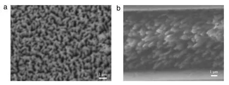
Fig.2.Speckle patterns on the CFRP sample surface after ion beam milling 6 h when the sample stage tilts(a)0°and(b)22°.
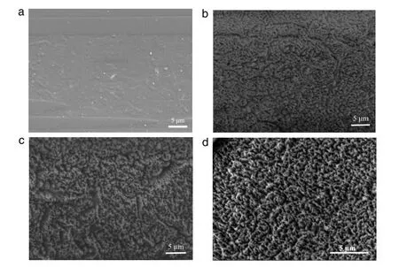
Fig.3.CFRP sample surface morphologies before and after ion beam milling,(a)before milling with an Au layer,(b)after 4 h,(c)after 5 h,and(d)after 6 h.
Figure 6(a)and(b)reveals different speckle morphology for the PI samples after milling 6 and 8 h,respectively.Most speckle patternsofPIsamplesaresmallandintensivewiththespecklesize from 20 to 700 nm.Since the nano speckle patterns in Fig.6(b)is easier to distinguish,8 h is chosen to be the optimum milling time for PI samples.
ItcanbeseenfromFigs.3-6,thelongermillingtimewillenlarge the speckle size for a specific material.The generated speckle is located in a circle area with a diameter of around 10 mm,which depends on the ion beam diameter and the distance from the ion gun to the sample surface.BIB milling is very simple,fast,and low-cost in producing nanoscale speckle in a large area of several millimeters compared with FIB milling and electron beam lithography.
To evaluate the time stability of the fabricated speckle,the CFRP specimen with the speckle pattern after ion beam milling for 6 h shown in Fig.3(d)was put in a Hitachi S-4800N SEM, and the speckle appearance was presented in Fig.7(a).The accelerated voltage was 20 kV,the working distance was 8.3 mm and the magnification was 6000×.A series of speckle images were recorded every 30 s.The histograms of the speckle patterns at 0, 210,420,and 600 s are displayed in Fig.7(b).The variations of the mean intensity and the standard deviation of the speckle pattern along with the time of duration is plotted in Fig.7(c).It can be seen that the mean intensity is around 110 and there is only a slight change during the period of 600 s.Based on the mean intensity at 0 s,the relative error of the mean intensity at 600 s is only 1.53%.The standard deviation of the intensity also changes slightly from 24.793 at 0 s to 25.265 at 600 s.It demonstrates that the fabricatedspecklepatternhasagoodtimestabilityandcanbeused for deformation measurement.
The fabricated nanoscale speckle pattern can be used to check the accuracy of the mechanical movement of an SEM sample stage. Asanexample,theaccuracyoftheFEIQUANTA200Ffieldemission SEMwiththeminimumtranslationdistanceof0.1µmwasstudied. In the experiment,the specimen stage was operated to translate for 0.1µm in the X direction and the speckle pattern images were recorded before and after translation.
The displacement between the two images was calculated by the DIC method using the vic-2D software as shown in Fig.8.The displacement distribution is relatively uniform.The average value of the full-field displacement is 0.11µm and the average full-field matching confidence is 0.01 pixel,which proved the accuracy ofcalculation.The error between the DIC calculation result 0.11µm and the translation distance of the sample stage 0.1µm reveals that the mechanical translation error of the SEM sample stage is around 10%.The fabricated speckle patterns have great potential in the accurate micro/nano deformation measurement.
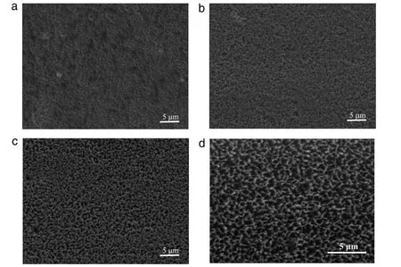
Fig.4.Polyvinyl formal-acetal sample surface morphologies after ion beam milling,(a)after 3 h,(b)after 4 h,(c)after 5 h,and(d)after 6 h.
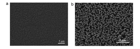
Fig.5.Polyester sample surface morphologies after ion beam milling,(a)after 4 h,(b)after 6 h.
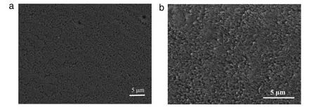
Fig.6.PI sample surface morphologies after ion beam milling,(a)after 6 h,(b)after 8 h.

Fig.7.Time stability of speckle pattern on CFRP during 600 s.
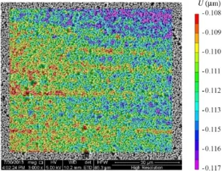
Fig.8.Displacement distribution of CFRP measured by the DIC method after the sample stage of SEM translate 0.1µm.
A fabrication technique of nanoscale speckle patterns on polymersusingBIBmillingwasproposed.Thistechniqueiscapable of producing speckles ranging from dozens of nanometers to a few micrometers in size in a circle area with a diameter of around 10 mm.The variations of the speckle patterns with the increases of the ion beam milling time and the tilt angle of the sample stage were investigated.It is easier to get a better speckle pattern whenthesamplestageisnottilted.Specklepatternswithdifferent morphologieswerefabricatedonthesurfaceoffourdifferentkinds of polymers.The speckle size on the PI samples is smaller than that on the other samples.The fabricated speckle has excellent time stability and can be used to check the mechanical translation error of an SEM using DIC.The proposed speckle fabrication method is useful in micro/nano-scale deformation analysis of polymers.
Acknowledgment
ThisworkwassupportedbyCross-ministerialStrategicInnovation Promotion Program(Unit D66)Innovative Measurement and AnalysisforStructuralMaterials(SIP-IMASM)operatedbytheCabinet Office,Japan.
[1]J.H.Qiu,T.Murata,X.L.Wu,et al.,Plastic deformation mechanism of crystallinepolymermaterialsduringtherollingprocess,J.Mater.Sci.48(2013)1920-1931.
[2]H.M.Xie,S.Kishimoto,Y.J.Li,Fabrication of micro-moire gratings on a strain sensor structure for deformation analysis with micro-moire technique, Microelectron.Reliab.49(2009)727-733.
[3]W.H.Peters,W.F.Ranson,Digital imaging techniques in experimental stress analysis,Opt.Eng.21(1982)427-431.
[4]M.A.Sutton,M.Q.Cheng,W.H.Peters,et al.,Application of an optimized digital correlation method to planar deformation analysis,Image Vision Comput.4(1986)143-150.
[5]T.C.Chu,W.Ranson,M.A.Sutton,Applications of digital-image correlation techniques to experimental mechanics,Exp.Mech.25(1985)232-244.
[6]B.Pan,Recent progress in digital image correlation,Exp.Mech.51(2011)1223-1235.
[7]M.A.Sutton,N.Li,D.Garcia,et al.,Metrology in a scanning electron microscope:Theoreticaldevelopmentsandexperimentalvalidation,Meas.Sci. Technol.17(2006)2613-2622.
[8]A.D.Kammers,S.Daly,Small-scale patterning methods for digital image correlation under scanning electron microscopy,Meas.Sci.Technol.22(2011)125501.
[9]B.Winiarski,G.S.Schajer,P.J.Withers,Surface decoration for improving the accuracy of displacement measurements by digital image correlation in SEM, Exp.Mech.51(2012)793-804.
[10]Z.B.Zhou,P.W.Chen,F.L.Huang,Experimental study on the micromechanical behavior of a PBX simulant using SEM and digital image correlation method, Opt.Laser Eng.49(2011)366-370.
[11]T.Hua,H.M.Xie,S.Wang,et al.,Evaluation of the quality of a speckle pattern in the digital image correlation method by mean subset fluctuation,Opt.Laser Technol.43(2011)9-13.
[12]Y.Tanaka,K.Naito,S.Kishimoto,et al.,Development of a pattern to measure multiscale deformation and strain distribution via in situ FE-SEM observation, Nanotechnology 22(2011)115704.
[13]Y.J.Li,H.M.Xie,Q.Luo,etal.,Fabricationtechniqueofmicro/nano-scalespeckle patterns with focused ion beam,Sci.China Phys.Mech.Astronom.55(2012)1037-1044.
[14]Z.W.Liu,H.M.Xie,D.N.Fang,et al.,Deformation analysis in microstructures and micro-devices,Microelectron.Reliab.47(2007)2226-2230.
[15]N.Li,S.M.Guo,M.A.Sutton,Recent Progress in E-beam Lithography for SEM Patterning,MEMS and Nanotechnology,in:Conference Proceedings of the Society for Experimental Mechanics Series,2011,pp.163-166.
[16]N.Sabate,D.Vogel,A.Gollhardt,et al.,Digital image correlation of nanoscale deformation fields for local stress measurement in thin films,Nanotechnology 17(2006)5264-5270.
[17]N.Sabate,D.Vogel,A.Gollhardt,et al.,Measurement of residual stress by slot milling with focused ion-beam equipment,J.Micromech.Microeng.16(2006)254-259.
[18]M.Sebastiani,C.Eberl,E.Bemporad,et al.,Depth resolved residual stress analysis of thin coatings by a new FIB-DIC method,Mater.Sci.Eng.A 528(2011)7901-7908.
[19]A.Korsunsky,M.Sebastiani,E.Bemporad,Residual stress evaluation at the micrometer scale:Analysis of thin coatings by FIB milling and digital image correlation,Surf.Coat.Technol.205(2010)2393-2403.
[20]T.A.Berfield,J.K.Patel,R.G.Shimmin,et al.,Micro-and nanoscale deformation measurement of surface and internal planes via digital image correlation,Exp. Mech.47(2007)51-62.
[21]W.A.Scrivens,Y.Luo,M.A.Sutton,et al.,Development of patterns for digital image correlation measurements at reduced length scales,Exp.Mech.47(2007)63-77.
[22]H.X.Wang,H.M.Xie,Y.J.Li,et al.,Fabrication of micro-scale speckle pattern and its applications for deformation measurement,Meas.Sci.Tech.23(2012)035402.
[23]N.Brodusch,K.Zaghib,R.Gauvin,Electron backscatter diffraction applied to lithium sheets prepared by broad ion beam milling,Microsc.Res.Tech.78(2015)30-39.
[24]B.J.Olanipekun,K.Azmy,Genesis and morphology of intracrystalline nanopores and mineral micro inclusions hosted in burial dolomite crystals: Application of broad ion beam-scanning electron microscope(BIB-SEM),Mar. Pet.Geol.74(2016)1-11.
11 May 2016
.
E-mail address:wang.qinghua@aist.go.jp(Q.Wang).
http://dx.doi.org/10.1016/j.taml.2016.07.001
2095-0349/©2016 The Authors.Published by Elsevier Ltd on behalf of The Chinese Society of Theoretical and Applied Mechanics.This is an open access article under the CC BY-NC-ND license(http://creativecommons.org/licenses/by-nc-nd/4.0/).
杂志排行
Theoretical & Applied Mechanics Letters的其它文章
- Editorial:Advances in Optical Techniques for Mechanical Measurements
- Residual stress measurement for injection molded componentsAchyut Adhikari∗,Thomas Bourgade,Anand Asundi
- Instantaneous phase-stepping interferometry based on a pixelated micro-polarizer arraySatoru Yoneyama∗,Shuichi Arikawa
- Visualizing surface strain distribution of facial skin using stereovisionNagisa Miura,Tsubasa Sakamoto,Yuichi Aoyagi,Satoru Yoneyama∗
- Fabrication of micro-scale gratings for moiré method with a femtosecond laserGaosheng Yana,Jianguo Zhua,∗,Yanlong Huanga,Wenfen Haoa,Yanjie Lib
- The mechanics and deformation of high temperature steel frame rapidly cooled by spray water in fire fightingYunchun Xia
