Epitaxial Growth and Thermoelectric Measurement of Bi2Te3/Sb Superlattice Nanowires
2016-07-05LingLiSichoXuGunghiLiKeyLbortoryofMterilsPhysicsAnhuiKeyLbortoryofNnomterilsndNnotechnologyInstituteofSolidSttePhysicsChineseAcdemyofSciencesHefei230031ChinSchoolofChemistryndMterilsScienceUniversityofSciencendTec
Ling Li,Si-cho Xu,Gung-hi Li,b∗. Key Lbortory of Mterils Physics,Anhui Key Lbortory of Nnomterils nd Nnotechnology,Institute of Solid Stte Physics,Chinese Acdemy of Sciences,Hefei 230031,Chin b. School of Chemistry nd Mterils Science,University of Science nd Technology of Chin,Hefei 230026,Chin
Epitaxial Growth and Thermoelectric Measurement of Bi2Te3/Sb Superlattice Nanowires
Liang Lia,Si-chao Xua,Guang-hai Lia,b∗
a. Key Laboratory of Materials Physics,Anhui Key Laboratory of Nanomaterials and Nanotechnology,Institute of Solid State Physics,Chinese Academy of Sciences,Hefei 230031,China b. School of Chemistry and Materials Science,University of Science and Technology of China,Hefei 230026,China
(Dated:Received on September 21,2015;Accepted on November 23,2015)
Superlattice nanowires are expected to show further enhanced thermoelectric performance compared with conventional nanowires or superlattice thin films. We report the epitaxial growth of high density Bi2Te3/Sb superlattice nanowire arrays with a very small bilayer thickness by pulse electrodeposition. Transmission electron microscopy,selected area electron diffraction and high resolution transmission electron microscopy were used to characterize the superlattice nanowires,and Harman technique was employed to measure the figure of merit(ZT)of the superlattice nanowire array in high vacuum condition. The superlattice nanowire arrays exhibit a ZT of 0.15 at 330 K,and a temperature difference of about 6.6 K can be realized across the nanowire arrays.
Key words:Bi2Te3,Superlattice nanowires,Electrodeposition,Thermoelectric,Harman technique
∗Author to whom correspondence should be addressed. E-mail:ghli@issp.ac.cn.
I. INTRODUCTION
There is growing interest in constructing thermoelectric microdevice for harvesting waste energy and refrigerating. The performance of such devices is determined by the efficiency of thermoelectric materials which is directly related to the dimensionless figure of merit (ZT):ZT=S2σT/κ,where S,σ,T,and κ are the Seebeck coefficient,electrical conductivity,absolute temperature,and thermal conductivity,respectively. The nanostructured materials have attracted much attention in thermoelectricity because they were predicated to have higher efficiencies than their bulk counterparts [1-4]. Studies on Bi2Te3/Sb2Te3[4]and Ge/Si0.5Ge0.5[5]superlattice thin films and Si nanowires[6,7]have shown that these nanostructured materials have an enhanced ZT in comparison with the corresponding bulks. On the other hand,compared to 2D superlattice thin films and 1D nanowires,the zero-dimensional structure of superlattice nanowires which integrates advantages of the enhanced phonon scattering at the interfaces between periodically alternating materials and the higher quantum confinement as well as a sharper density of states may lead to further improvement in ZT[8-10].
The template-based electrodeposition method is a widely used technique for fabricating nanowire array because it has some advantages such as simple operation, low cost,high controllability. Electrodeposited materials can potentially be integrated into nanogenerators or Peltier coolers[10-12]. A variety of thermoelectric superlattice nanowires such as Bi/Sb[13],Bi/BiSb[10,14],BiTe/BiSbTe[9],Bi2Te3/Sb[15],Bi2Te3/Te[16],Bi2Te2Se/Te[17],and Bi2Te3/Bi[18]have been fabricated using this simple technique. For near room temperature applications,the Bi2Te3related superlattice nanowires are always the best choice. Unfortunately,the Bi2Te3related superlattice nanowires obtained so far are always polycrystalline[9,15],which may depress the electrical conductivity of the superlattice nanowires. Although various types of thermoelectric superlattice nanowires have been fabricated,there is still no report on the thermoelectric performance of the abovementioned superlattice nanowire. In this work,we report the epitaxial growth of Bi2Te3/Sb superlattice nanowires by pulsed electrodeposition and thermoelectric characterization of the nanowire arrays via Harman technique.
II. EXPERIMENTS
Anodic alumina membrane(AAM)was prepared using a two-step anodic anodization process as described previously[19-22]. Electrodeposition was carried out in a three-electrode electrochemical cell,where a piece of graphite,saturated calomel electrode,and Ausputtered AAMs served as counter,reference and working electrode,respectively. Before electrodeposition,about 2µm-length Au nanorods were first deposited in an electrolyte containing 0.005 mol/L HAuCl4·4H2O and 0.5 mol/L boric acid. The electrolyte for the deposition of Bi2Te3/Sb superlattice nanowires contained 1 mol/L HNO3,0.008 mol/L Bi(NO3)3·5H2O,0.015 mol/L TeO2,0.02 mol/L Sb2O3,and 0.3 mol/L tartaric acid. Cyclic voltammogram(CV)experiments were performed to determine the suitable deposition voltages for the deposition of Bi2Te3and Sb.
The microstructure and morphology of the nanowires were examined by transmission electron microscopy (TEM,H-800),selected area electron diffraction (SAED),and high-resolution transmission electron microscopy(HRTEM,JEOL-2010).
The Harman method was used to measure the ZT of the nanowire arrays[23-28]. Before measurement,a top Au electrode segment with a length of about 2µm was electrodeposited onto the nanowire tips immediately after the deposition of Bi2Te3/Sb superlattice nanowires,this step is very important to get a highly ohmic contact. As shown in Fig.1(a),when a DC current IDCis applied to the nanowire array,a temperature difference is established across the nanowire array due to the Peltier effect. After the system reaches a steady state,the total measured voltage is the sum of the ohmic and Seebeck voltages[26]:

where Vohmicis the voltage drop due to the resistive nature of the nanowires which can be measured using the the AC measurement[26],and VSeebeckis the Seebeck voltage induced by Peltier effect. Then the ZT of the nanowire array can be calculated using the following formula[23,26]:

where VDCand VACis respectively the DC and AC voltage.
The measurement scheme for evaluating the heating or cooling ability of the fabricated superlattice nanowire arrays in air condition is shown in Fig.2. Briefly,the nanowire array was sandwich between two Cu blocks,and then a continued DC current was applied across the array for about 1 min,a pair of 80µm K-type thermocouple wires was attached to the two sides of the array for the measurement of temperature difference∆T.
III. RESULTS AND DISCUSSION
In Fig.3,two obvious reduction peaks(the labeled A and B)and three oxidation peaks(C,D,and E)were observed. Peak A at around -0.1 V can be attributed to the deposition of Bi-Te alloy,and the peak B at around -0.35 V accounts for the abundant electrodeposition of a Bi-Sb-Te ternary alloy. We found that the Bi2Te3binary alloy and Sb elementary can be deposited at the potential of -0.06 and -0.35 V,respectively,and the Bi-Te binary alloys instead of Bi2Te3binary alloy and Sb elementary were obtained at other potentials. The chemical compositions of the resulted Bi-Te binary alloy and Sb nanowires were measured by inductively coupled plasma atomic emission spectroscopy(ICP-AES,Thermo iCAP 6300). The nanowires deposited at -0.06 V exhibit a composition of 37.1%Bi,2.3%Sb,and 60.6%Te,which is close to the stoichiometric binary alloy Bi2Te3with a slightly doped-Sb,and the nanowires deposited at -0.35 V have a composition of 3.1%Bi,87.1%Sb,and 9.8%Te,indicating the majority element deposited at this potential is Sb.
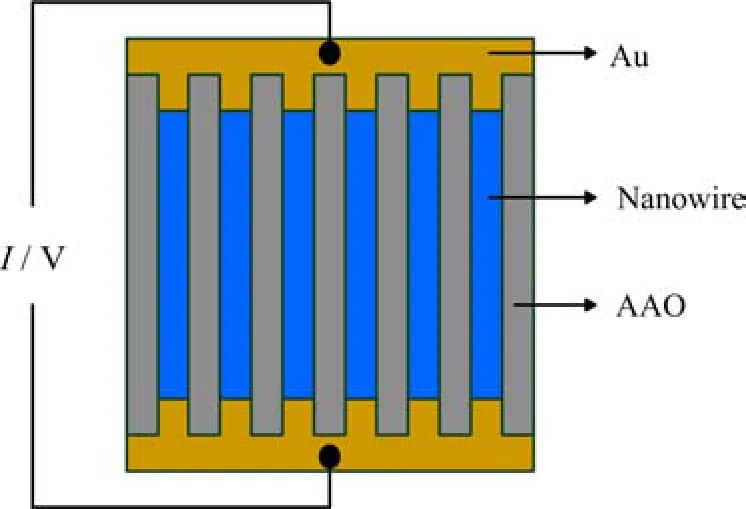
FIG. 1 Schematic of the AC and DC measurement of the Bi2Te3/Sb superlattice nanowire array.
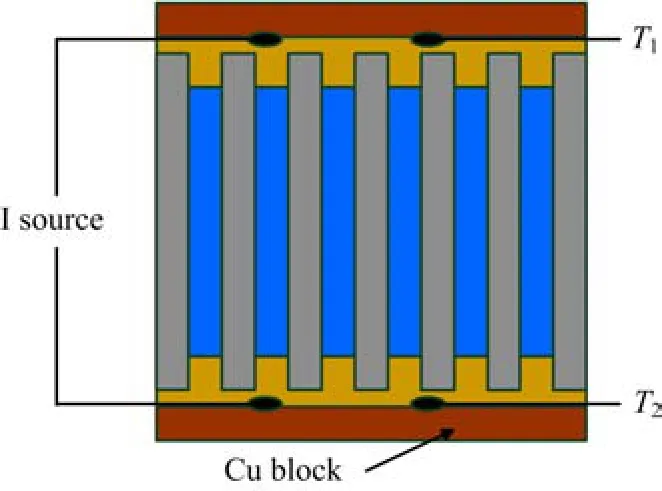
FIG. 2 Schematic of the measurement for evaluating heating ability of the Bi2Te3/Sb superlattice nanowire array.
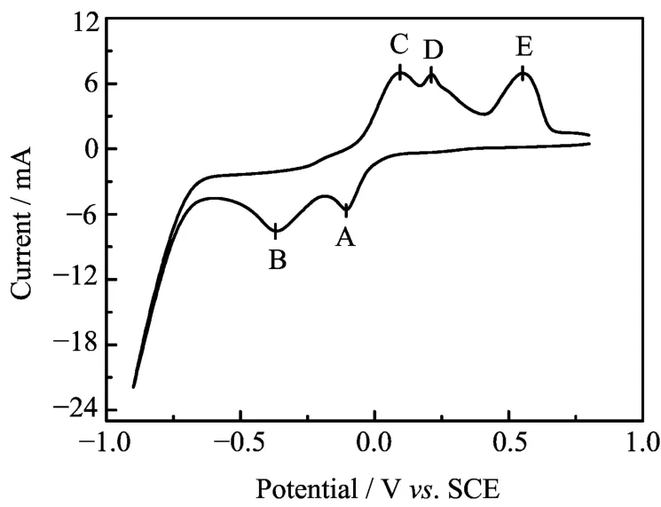
FIG. 3 CV curve of the electrolyte at a scan rate of 40 mV/s.
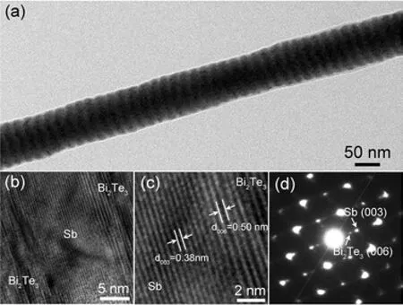
FIG. 4 (a)TEM image of an individual Bi2Te3/Sb superlattice nanowire,(b)and(c)HRTEM images of the junction of the superlattice nanowire,(d)the corresponding SAED pattern of(a).
Figure 4(a)shows transmission electron microscopy (TEM,H-800)image of the Bi2Te3/Sb superlattice nanowires pulsed electrodeposited at -0.06 and -0.35 V with the pulse duration 6 and 2 s,respectively. One can see that the average diameter of the nanowires is about 80 nm,and equals to the pore size of the AAM used. Due to the mass difference,the Bi2Te3and Sb segments can be clearly distinguished by the bright field TEM imaging in which the darker parts with a length of about 12 nm correspond to Bi2Te3segments and the brighter ones with a length of about 10 nm correspond to Sb segments. The bilayer thickness of Bi2Te3and Sb segments is about 22 nm,which demonstrating that the Bi2Te3/Sb superlattice nanowires fabricated by above mentioned depositing parameters have very small bilayer thickness. Figure 4(b)shows an HRTEM image taken at the junction region of the Bi2Te3and Sb segments,and the magnifying image is shown in Fig.4(c). The observed lattice spacings of 0.38 and 0.5 nm in Fig.4(c)correspond respectively to the(003)plane of Sb and(006)plane of Bi2Te3,indicating that the single crystalline Sb segment of a rhombohedral phase grows along[003]direction and Bi2Te3segment of a rhombohedral phase is along[006]direction. Bi2Te3has the crystal parameters of a=0.4417 nm and c=2.984 nm,while Sb has the crystal parameters of a=0.4307 nm and c=1.1273 nm,and both of them belong to the rhombohedral space group R¯3m[19,29],from these facts one can conclude that the deposition of the Bi2Te3/Sb superlattice nanowires is truly an epitaxial growth. The presence of double diffraction spots in the corresponding SAED pattern shown in Fig.4(d)further demonstrates the epitaxial character of the superlattice nanowires.
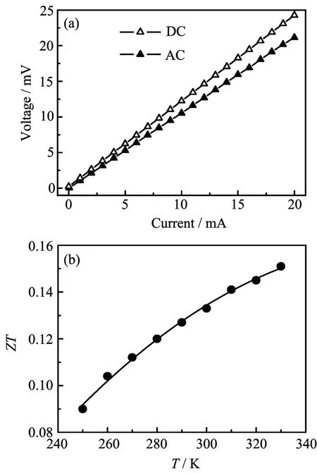
FIG. 5 (a)I-V curves of the nanowire array at 300 K and (b)temperature dependence of the calculated ZT.
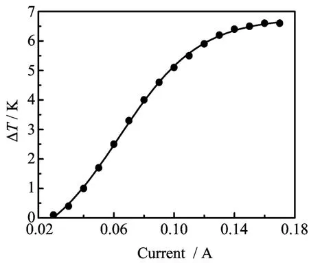
FIG. 6 The dependence of the temperature difference,∆T,across the array on applied DC current.
The AC and DC measurements were taken at a 1×10⁻⁴Pa high vacuum pressure. In order to reach a steady state,a stabilization time of 20 min was used at each temperature before measurement. For DC measurement,the bias current was applied for about 1 min before record the voltage data. Figure 5(a)shows the I-V curves of AC and DC measurements at 300 K,a nearly linear relationship between current and voltage can be clearly seen,indicating a highly ohmic contact of the nanowires. From Fig.5(b),one can also see that the VDCis always higher than VACat the same input current,which is reasonable if one considers the Peltier effect in the thermoelectric superlattice nanowires. Figure 5(b)shows the calculated ZT from 250 K to 330 K from Eq.(2),in which the highest ZT is about 0.15 at 330 K. At 300 K,the measured ZT is only about 0.13 and is much less than the state-of-the-art commercial Bi2Te3bulk(with ZT of about 1). Several reasons may be responsible for the low ZT:(i)the composition of each segment of the superlattice nanowires is not in the optimum region,which further leads the carrier concentration out of the optimum region[30],(ii)the thermal conductivity of AAM cannot be neglected compared to the nanowires[24,31],and thus the measured VSeebeckis always lower than the truly one. In the future,we aim to optimize the performance of the superlattice nanowires by regulating the composition (i.e.,Bi2Te3/Sb2Te3superlattice nanowires)and using very low thermal conductivity supporting membrane (i.e.,ion track Membranes)[32].
Figure 6 shows the temperature difference between the top and back side of the Bi2Te3/Sb superlattice nanowire array to illustrate the heating ability of the thermoelectric microdevice. One can see that ∆T first increases with increasing from zero at applied current of 0.02 A,and then reaches a steady value of about 6.6 K at about 0.16 A,this temperature difference is near the value obtained in hybrid Bi0.3Sb0.7nanowire/Bi0.4Sb1.6Te bulk thermoelectric couple. With further increasing current to over 0.2 A,because of breakdown of the electronic contact,no data can be obtained. This result clearly demonstrates that the Bi2Te3/Sb superlattice nanowire array can create a much larger temperature difference compared to the superlattice nanowire/alumina composite and can be used as potential thermoelectric microdevice.
IV. CONCLUSION
Thermoelectric Bi2Te3/Sb superlattice nanowires with a very small bilayer thickness have been grown by pulse electrodeposition technique. The highest ZT of the superlattice nanowire arrays measured in high vacuum condition using Harman method was 0.15 at 330 K,and the highest temperature difference across the nanowire arrays in air condition is about 6.6 K. We believe that with further optimizing the growth condition,the superlattice nanowires will have an even high ZT and can be incorporated into a heating or cooling device.
V. ACKNOWLEDGMENTS
This work was supported by the National Natural Science Foundation of China(No.11174285).
[1]L. D. Hicks and M. S. Dresselhaus,Phys. Rev. B 47,16631(1993).
[2]L. Hicks and M. Dresselhaus,Phys. Rev. B 47,12727 (1993).
[3]L. Li,N. Koshizaki,and G. H. Li,J. Mater. Sci. Tech. 24,550(2008).
[4]R. Venkatasubramanian,E. Siivola,T. Colpitts,and B. O'quinn,Nature 413,597(2001).
[5]L. F. Llin,A. Samarelli,S. Cecchi,T. Etzelstorfer,E. M. Gubler,D. Chrastina,G. Isella,J. Stangl,J. M. R. Weaver,and P. S. Dobson,Appl. Phys. Lett. 103,143507(2013).
[6]A. I. Boukai,Y. Bunimovich,J. Tahir-Kheli,J. K. Yu,W. A. Goddard Iii,and J. R. Heath,Nature 451,168 (2008).
[7]A. I. Hochbaum,R. Chen,R. D. Delgado,W. Liang,E. C. Garnett,M. Najarian,A. Majumdar,and P. Yang,Nature 451,163(2008).
[8]Y. M. Lin and M. S. Dresselhaus,Phys. Rev. B 68,075304(2003).
[9]B. Yoo,F. Xiao,K. N. Bozhilov,J. Herman,M. A. Ryan,and N. V. Myung,Adv. Mater. 19,296(2007).
[10]X. C. Dou,G. H. Li,and H. C. Lei,Nano Lett. 8,1286 (2008).
[11]N. Peranio,E. Leister,W. T¨ollner,O. Eibl,and K. Nielsch,Adv. Funct. Mater. 22,151(2012).
[12]L. Li,G. H. Li,X. D. Wang,and Z. M. M. Wang,Nanoscale Thermoelectrics,New York:Springer,237,(2014).
[13]F. H. Xue,G. T. Fei,B. Wu,P. Cui,and L. D. Zhang,J. Am. Chem. Soc. 127,15348(2005).
[14]X. Dou,G. Li,H. Lei,X. Huang,L. Li,and I. W. Boyd,J. Electrochem. Soc. 156,K149(2009).
[15]W. Wang,G. Zhang,and X. Li,J. Phys. Chem. C 112,15190(2008).
[16]W. Wang,X. Lu,T. Zhang,G. Zhang,W. Jiang,and X. Li,J. Am. Chem. Soc. 129,6702(2007).
[17]X. L. Li,K. F. Cai,D. H. Yu,and Y. Y. Wang,Superlatt. Microstruct. 50,557(2011).
[18]Z. Xue,X. L. Li,and D. M. Yu,Superlatt. Microstruct. 74,273(2014).
[19]Y. Zhang,G. H. Li,Y. C. Wu,B. Zhang,W. H. Song,and L. D. Zhang,Adv. Mater. 14,1227(2002).
[20]L. Li,Y. W. Yang,X. H. Huang,G. H. Li,R. Ang,and L. D. Zhang,Appl. Phys. Lett. 88,103119(2006).
[21]L. Li,G. H. Li,Y. Zhang,Y. W. Yang,and L. D. Zhang,J. Phys. Chem. B 108,19380(1998).
[22]L. Li,Y. W. Yang,G. H. Li,and L. D. Zhang,Small 2,548(2006).
[23]T. C. Harman,J. Appl. Phys. 29,1373(1958).
[24]J. Keyani,A. M. Stacy,and J. Sharp,Appl. Phys. Lett. 89,233106(2006).
[25]D. Pinisetty,M. Gupta,A. B. Karki,D. P. Young,and R. V. Devireddy,J. Mater. Chem. 21,4098(2011).
[26]R. Chavez,A. Becker,M. Bartel,V. Kessler,G. Schierning,and R. Schmechel,Rev. Sci. Instrum. 84,106106 (2013).
[27]T. Favaloro,A. Ziabari,J. H. Bahk,P. Burke,H. Lu,J. Bowers,A. Gossard,Z. Bian,and A. Shakouri,J. Appl. Phys. 11,034501(2014).
[28]S. Keun´aKim,Phys. Chem. Chem. Phys. 16,3529 (2014).
[29]L. Li,Y. W. Yang,X. H. Huang,G. H. Li,and L. D. Zhang,Nanotechnology 17,1706(2006).
[30]J. H. Zhou,C. G. Jin,J. H. Seol,X. G. Li,and L. Shi,Appl. Phys. Lett. 87,133109(2005).
[31]D. A. Borca-Tasciuc and G. Chen,J. Appl. Phys. 97,084303(2005).
[32]O. Picht,S. M¨uller,I. Alber,M. Rauber,J. Lensch-Falk,D. L. Medlin,R. Neumann,and M. E. Toimil-Molares,J. Phys. Chem. C 116,5367(2012).
DOI:10.1063/1674-0068/29/cjcp1509194
杂志排行
CHINESE JOURNAL OF CHEMICAL PHYSICS的其它文章
- Virtual Screening of Human O-GlcNAc Transferase Inhibitors
- Spin Polarization at Organic-Ferromagnetic Interface:Effect of Contact Configuration
- Comparative Theoretical Studies on Several Energetic Substituted Dioxin-imidazole Derivatives
- Controlled Synthesis of PCL/PVP Copolymer by RAFT Method and Its Hydrophilic Block-Dependent Micellar Behaviors
- Morphology and Growth Process of Bat-like ZnO Crystals by Thermal Evaporation
- Investigation of Ultrafast Electronic Transfer Process on Organic/Inorganic Heterojunction by Femtosecond Transient Absorption
