Fabricating Nanogaps between Nanoelectrodes using Dielectrophoresis Technique for Molecular Fluorescence Enhancement
2016-07-05QiushiMengHongbingCaiKeLinSanZhuYuanLiaoYangZhangXiaopingWangZhenchaoDongHefeiNationalLaboratoryforPhysicalSciencesattheMicroscaleandSynergeticInnovationCenterofQuantumInformationandQuantumPhysicsUniversityofScience
Qiu-shi Meng,Hong-bing Cai,Ke Lin,San-e Zhu,Yuan Liao,Yang Zhang,Xiao-ping Wang,Zhen-chao DongHefei National Laboratory for Physical Sciences at the Microscale,and Synergetic Innovation Center of Quantum Information and Quantum Physics,University of Science and Technology of China,Hefei 230026,China
Fabricating Nanogaps between Nanoelectrodes using Dielectrophoresis Technique for Molecular Fluorescence Enhancement
Qiu-shi Meng,Hong-bing Cai,Ke Lin,San-e Zhu,Yuan Liao,Yang Zhang∗,Xiao-ping Wang,Zhen-chao Dong∗
Hefei National Laboratory for Physical Sciences at the Microscale,and Synergetic Innovation Center of Quantum Information and Quantum Physics,University of Science and Technology of China,Hefei 230026,China
(Dated:Received on October 30,2015;Accepted on November 27,2015)
Here we demonstrate the fabrication of nanometer-sized gaps by assembling single coreshell nanoparticles between metallic nanoelectrodes. Protein coated SiO2@Au coreshell nanoparticles are synthesized and positioned between fluorescent molecules-covered electrodes in a controllable way using dielectrophoretic trapping,forming nanogaps sandwiched between nanoparticle and nanoelectrodes. Preliminary photoluminescence measurements show that enhanced molecular fluorescence could be detected from the fluorescent molecules inside the nanogaps. These results pave the way for realizing electrically driven molecular fluorescence based on nanogap electrodes.
Key words:Nanogap,Nanoelectrode,Dielectrophoresis,Coreshell nanoparticle,Fluorescence enhancement
∗Authors to whom correspondence should be addressed. E-mail:zcdong@ustc.edu.cn,zhyangnano@ustc.edu.cn
I. INTRODUCTION
The research on nanometer-sized gaps(nanogaps)between metallic nanoelectrodes has attracted considerable attention because of their broad applications in molecular electronics[1,2]and optoelectronics[3-6]. One of the interesting applications is to realize electrically driven molecular emission by exploiting the plasmonic enhancement in the nanogap. The first step is to fabricate nanogaps between metallic nanoelectrodes,and various methods have been proposed,such as electron beam lithography(EBL)[7],mechanical break junction[8],electromigration[9],and dielectrophoresis (DEP)[10]. Among them,the DEP technique allows to fabricate nanogaps sandwiched between nanoparticles and nanoelectrodes with controlled nanogap size down to the molecular scale[11,12],and is therefore adopted in the present work. In order to take advantage of plasmonic enhancement in the nanogaps but without suffering the fluorescence quenching problem,protein-coated SiO2@Au coreshell nanoparticles and self-decoupled fluorescent molecules are designed and used for the formation of molecular junctions. Moreover,the molecular fluorescence enhancement from the molecules inside the as-fabricated nanogaps is also explored preliminarily by photoluminescence measurements.

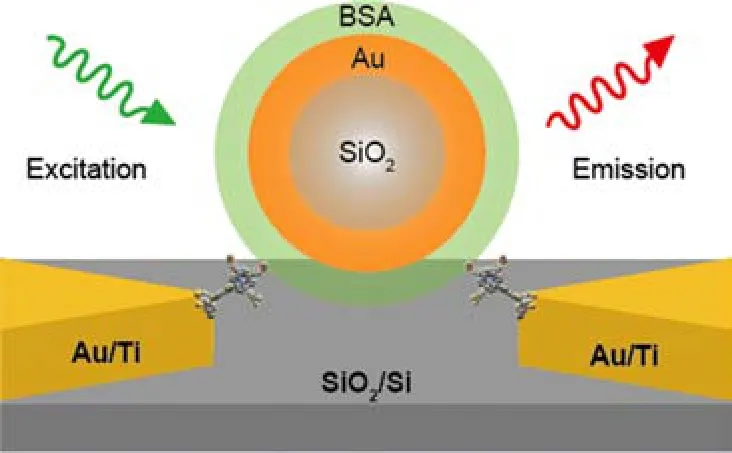
FIG. 1 Schematic of the nanogaps confined between a protein-coated coreshell nanoparticle and fluorescent molecule-functionalized nanoelectrodes.
II. SAMPLE DESIGN
Figure 1 shows the schematic of nanogaps with nanoparticle-molecule-nanoelectrode structure. Our strategy is to trap a single coreshell nanoparticle between a pair of metallic(Au/Ti)electrodes covered with a self-assembled monolayer(SAM)of functionalized fluorescent molecules,and thus to form nanogaps at single molecular scale on both sides.
The use of the SiO2@Au coreshell nanoparticles in the nanogap structure is because of the following two reasons:(i)the plasmonic resonance of coreshell nanoparticles can be tuned over a large spectral range[13],which will be favorable for generating large fluorescence enhancements;(ii)the coreshell nanoparticles can be made relatively large(around several hundred nanometers in diameter)[14],which can facilitate the positioning of a single nanoparticle between a pair of nanoelec-trodes[15],avoiding the coalescence of nanoparticles during the DEP process and also reducing the difficulty in making ultra-small inter-electrode nanogaps by EBL.
Besides,in order to avoid molecular fluorescence quenching due to the presence of nearby metallic surfaces,the fluorophores are decoupled from the metallic nanoelectrodes by functionalized spacer groups of tripodal porphyrin(TPP-3Ac)molecules[16],while the metallic surface of coreshell nanoparticles are coated by bull serum albumin(BSA)protein layers[17].

FIG. 2 (a)Flowchart of synthesizing the BSA-coated SiO2@Au coreshell nanoparticles and the corresponding TEM image. (b)SEM image of a pair of Au/Ti electrodes patterned by EBL with a predefined gap of 250 nm. Inset:optical microscope image of the electrode array.(c)Photoluminescence spectrum of TPP-3Ac molecules in CH2Cl2solution(~1.0µmol/L). TPP-3Ac molecules are used for the molecular assembly process. Inset:the chemical structure of the TPP-3Ac molecule. (d)Schematic of the experimental set-up used for the DEP trapping of coreshell nanoparticles.
III. SAMPLE PREPARATIONS AND EXPERIMENTAL CONDITIONS
A. Fabrication of the BSA-coated coreshell nanoparticles
SiO2@Au coreshell particles were synthesized according to Ref.[18],as shown in Fig.2(a). Silica nanosphere cores were prepared by the hydrolysis of tetraethylorthosilicate(TEOS)in the mixture of ammonia and ethanol solution via the St¨ober method. After being functionalized with 3-aminopropyl triethoxysilane(APTES),the amine-terminated silica nanospheres were mixed together with the pre-prepared colloidal gold nanoparticles(~2 nm)for the attachment of the gold“seeds”. Then by reducing gold from a HAuCl4solution(1%)with formaldehyde,continuous gold shells grew from the attached“seeds”all over the silica nanospheres and the coreshell nanoparticles were formed. In order to remove the residual reaction byproducts,the synthesized nano-coreshell nanoparticles were washed sufficiently through centrifugation and re-dispersed in deionized water.
Before DEP trapping,the coreshell nanoparticles were coated with BSA protein layers. In this step,the synthesized coreshell nanoparticles were centrifuged and then mixed with 50µmol/L BSA aqueous buffer solutions at room temperature for about 24 h. Finally,the mixture was centrifuged at very low speed to remove excess protein and re-dispersed in deionized water. As shown in the TEM image in Fig.2(a)(bottom left),the coreshell nanoparticles have been successfully synthesized with a total diameter of~500 nm(the SiO2core diameter is~410 nm,the thickness of Au shell is~90 nm and the thickness of BSA capping layer is 3-40 nm).
B. Preparation of the nanoelectrode
The metallic electrode array was fabricated using standard EBL combined with photolithography on Si substrates covered by 300-nm thick silicon oxides. Firstly,photolithography was used to pattern the larger contact pads(10 nm Ti/150 nm Au),of which the extended length is 4 mm and the width varied gradually from 20µm to 150µm. Secondly,standard EBL(Raith,e-Line)and lift-off technique were used to pattern the nanoelectrode structures(3 nm Ti/30 nm Au),defining an interelectrode separation of 250 nm. Scanningelectron microscopy(SEM)image and optical microscope image of the prepared nanoelectrodes are shown in Fig.2(b).
C. Molecular self-assembly on the nanoelectrode
TPP-3Ac was chosen as the emitter molecule for its specially designed self-decoupling function,of which the details have been described in Ref.[16]. The rigid tripodal anchor groups of the TPP-3AC molecule not only allow the formation of three robust Au-S bonds to fix the molecule to Au electrodes,but also serve as the decoupling spacer together with a linking ethynyl unit to separate the porphyrin fluorophore from the underlying metallic surface to suppress quenching. Figure 2(c)shows the photoluminescence(PL)spectrum of TPP-3Ac molecules in CH2Cl2solution(~1µmol/L),which is characterized by two emission peaks at about 660 nm (Qx(0,0))and 720 nm(Qx(0,1))[16].
Prior to the assembling procedure,the as-prepared metallic electrodes were cleaned for 5 min using O2plasma to remove organic residues and rinsed with ethanol for 10 min to remove gold oxides[19]. The sample was then blow dried with nitrogen gas and immersed into the TPP-3Ac solution for 12 h at room temperature for molecular assembly. Finally,the sample was taken out,rinsed thoroughly with CH2Cl2and blown dried with nitrogen gas.
D. Dielectrophoretic trapping of the coreshell nanoparticles
For the DEP trapping process shown in Fig.2(d),freshly prepared BSA-coated coreshell nanoparticles(~500 nm)and SAM-covered electrodes were employed. The external pads of the nanoelectrodes were electrically connected to a function generator(Tektronix AFG 3102)using Pt probe needles in a probe station. A drop(~5µL)of the aqueous solution of the BSA-coated coreshell nanoparticles was dispersed on the nanoelectrodes,covering the gap region. An alternating voltage of 1.5-2.0 V peak-peak at a frequency of 10 kHz was applied for 30-60 s for DEP trapping. After that,the sample was immediately rinsed thoroughly with deionized water and blow dried with nitrogen gas.
E. SEM characterization and fluorescence measurement
The SEM images were obtained by the same EBL system at a voltage(EHT)of 10 kV. For the fluorescence measurements,spatial maps of the integrated emission light were obtained using a WITec alpha300 scanning confocal fluorescence microscope in reflection mode,with the excitation laser at 532 nm(1.6 mW power). The corresponding optical spectra were recorded by an air-cooled charge-coupled-device(CCD)spectrometer (Princeton Instruments,ProEM CCD). All the fluorescence spectra presented in the work were not corrected for the wavelength-dependent sensitivity of photon collection and detection for our systems.

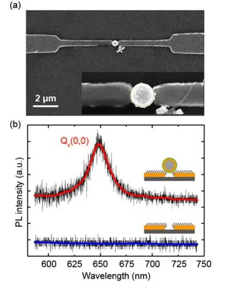
FIG. 3 (a)SEM image of a single BSA-coated SiO2@Au nanoparticle(500 nm)trapped in a 250 nm gap between an electrode pair.(b)Fluorescence spectra collected from the interelectrode nanogap area before(blue)and after(red)trapping with nanoparticles.
IV. RESULTS AND DISCUSSION
Following the DEP procedures described above,single SiO2@Au coreshell nanoparticles with a diameter of about 500 nm can be trapped between the SAM-covered electrodes,as shown in the SEM image of Fig.3(a). The successful trapping of single nanoparticles can be controlled by modulating the DEP parameters,i.e.,ac frequency,peak-to-peak voltage,and the trapping time [20]. In our system,the success rate of trapping single coreshell nanoparticles(500 nm in diameter)is about 10%under the optimized experimental parameters mentioned above.
Preliminary photoluminescence measurements were performed over the as-prepared samples. As shown in Fig.3(b),almost no discernable emission signals were detected from the TPP-3Ac molecules adsorbed on the area of nanoparticle-free electrode pairs,while an evidently enhanced emission peak at~650 nm was observed for the sample trapped with a coreshell nanoparticle. Such difference suggests that the occurrence of fluorescence is related to the formation of nanogaps between the trapped nanoparticle and the nanoelectrodepairs,which produces the fluorescence enhancement effect.
The photon map with the emission intensity given to each pixel could further help to identify the origin of the emission. As shown in Fig.4(a),the featureless characters in the photon map and emission spectrum collected from the molecule-free samples suggest that the emission peak at about 650 nm is originated from the Qx(0,0)emission of TPP-3Ac molecules rather than the plasmonic scattering of the nanogaps. On the other hand,as shown in Fig.4(b)for the sample with a single BSA-coated coreshell nanoparticle trapped in the gap between the TPP-3Ac SAM functionalized nanoelectrode pair,intense molecular fluorescence emission was observed when exciting the nanogap area between the nanoparticle and the nanoelectrode pairs,which indicates that the formation of nanogaps between coreshell nanoparticle and nanoelectrodes indeed offers strong fluorescence enhancement for the TPP-3Ac molecules adsorbed in the nanogaps(restricted by the diffraction limit,it is not possible to distinguish the two nanogap areas on either side of the nanoparticle). It should be noted that the Qx(0,1)emission from the TPP-3Ac molecules in the nanogaps is almost indiscernible,which might be related to the mismatch between the Qx(0,1)emission and the localized surface plasmon modes in the nanogaps[21]. Further research is underway.

FIG. 4 (a)Upper:SEM image of the molecule-free electrode pair with single BSA-coated coreshell nanoparticle trapped in the gap. Middle:photon map of emission intensities(integrated from 640 nm to 660 nm)acquired from the sample shown in upper SEM image. Lower:acquired fluorescence spectrum when exciting at the white“+”position indicated in the photon map.(b)Upper:SEM image of the the TPP-3Ac SAM-functionalized nanoelectrode pair with single BSA-coated coreshell nanoparticle trapped in the gap. Middle:photon map of emission intensities(integrated from 640 nm to 660 nm)acquired from the sample shown in upper SEM image. Lower:acquired fluorescence spectrum when exciting at the white “+”position indicated in the photon map. In the photon maps,stronger integrated intensities are represented in red,while weaker integrated intensities are represented in purple.
V. CONCLUSION
We have successfully positioned single BSA-coated coreshell nanoparticles between fluorophorefunctionalized metallic nanoelectrodes by the DEP trapping technique. This method provides a controllable way to fabricate nanogaps at the molecular scale. Preliminary fluorescence measurements on the nanoparticle-molecule-nanoelectrode structures show evident enhancement effect on the fluorescence from the molecules confined in the nanogaps. These results pave the way for realizing electrically driven molecular fluorescence based on nanogap electrodes and provide useful information for the development of optoelectronic nanodevices.
VI. ACKNOWLEDGMENTS
This work is supported by the National Basic Research Program of China,the National Natural Science Foundation of China,and Chinese Academy of Sciences.
[1]H. Park,J. Park,A. K. L. Lim,E. H. Anderson,A. P. Alivisatos,and P. L. McEuen,Nature 407,57(2000).
[2]S. Kubatkin,A. Danilov,M. Hjort,J. Cornil,J. L. Bredas,N. Stuhr-Hansen,P. Hedegard,and T. Bjornholm,Nature 425,698(2003).
[3]T. H. Lee,J. I. Gonzalez,J. Zheng,and R. M. Dickson,Acc. Chem. Res. 38,534(2005).
[4]C. W. Marquardt,S. Grunder,A. Blaszczyk,S. Dehm,F. Hennrich,H. von Lohneysen,M. Mayor,and R. Krupke,Nature Nanotech. 5,863(2010).
[5]Z. C. Dong,X. L. Guo,A. S. Trifonov,P. S. Dorozhkin,K. Miki,K. Kimura,S. Yokoyama,and S. Mashiko,Phys. Rev. Lett. 92,868011(2004).
[6]W. P. Hu,H. Nakashima,K. Furukawa,Y. Kashimura,K. Ajito,Y. Q. Liu,D. B. Zhu,and K. Torimitsu,J. Am. Chem. Soc. 127,2804(2005).
[7]W. Chen,H. Ahmed,and K. Nakazoto,Appl. Phys. Lett. 66,3383(1995).
[8]M. A. Reed,C. Zhou,C. J. Muller,T. P. Burgin,and J. M. Tour,Science 278,252(1997).
[9]H. Park,A. K. L. Lim,A. P. Alivisatos,J. Park,and P. L. McEuen,Appl. Phys. Lett. 75,301(1999).
[10]I. Amlani,A. M. Rawlett,L. A. Nagahara,and R. K. Tsui,Appl. Phys. Lett. 80,2761(2002).
[11]T. Dadosh,Y. Gordin,R. Krahne,I. Khivrich,D. Mahalu,V. Frydman,J. Sperling,A. Yacoby,and I. Bar-Joseph,Nature 436,677(2005).
[12]S. H. Hong,H. K. Kim,K. H. Cho,S. W. Hwang,J. S. Hwang,and D. Ahn,J. Vac. Sci. Technol. B 24,136 (2006).
[13]F. Tam,G. P. Goodrich,B. R. Johnson,and N. J. Halas,Nano. Lett. 7,496(2007).
[14]S. J. Oldenburg,R. D. Averitt,S. L. Westcott,and N. J. Halas,Chem. Phys. Lett. 288,243(1998).
[15]D. Cheon,S. Kumar,and G. H. Kim,Appl. Phys. Lett. 96,013101(2010).
[16]S. E. Zhu,Y. M. Kuang,F. Geng,J. Z. Zhu,C. Z. Wang,Y. J. Yu,Y. Luo,Y. Xiao,K. Q. Liu,Q. S. Meng,L. Zhang,S. Jiang,Y. Zhang,G. W. Wang,Z. C. Dong,and J. G. Hou,J. Am. Chem. Soc. 135,15794 (2013).
[17]R. Bardhan,N. K. Grady,J. R. Cole,A. Joshi,and N. J. Halas,Acs Nano 3,744(2009).
[18]T. Pham,J. B. Jackson,N. J. Halas,and T. R. Lee,Langmuir 18,4915(2002).
[19]H. Ron,S. Matlis,and I. Rubinstein,Langmuir 14,1116(1998).
[20]R. J. Barsotti Jr.,M. D. Vahey,R. Wartena,Y. M. Chiang,J. Voldman,and F. Stellacci,Small 3,488(2007).
[21]Z. C. Dong,X. L. Zhang,H. Y. Gao,Y. Luo,C. Zhang,L. G. Chen,R. Zhang,X. Tao,Y. Zhang,J. L. Yang,and J. G. Hou,Nature Photon. 4,50(2010).
DOI:10.1063/1674-0068/29/cjcp1510223
杂志排行
CHINESE JOURNAL OF CHEMICAL PHYSICS的其它文章
- Virtual Screening of Human O-GlcNAc Transferase Inhibitors
- Comparative Theoretical Studies on Several Energetic Substituted Dioxin-imidazole Derivatives
- Controlled Synthesis of PCL/PVP Copolymer by RAFT Method and Its Hydrophilic Block-Dependent Micellar Behaviors
- Epitaxial Growth and Thermoelectric Measurement of Bi2Te3/Sb Superlattice Nanowires
- Morphology and Growth Process of Bat-like ZnO Crystals by Thermal Evaporation
- Investigation of Ultrafast Electronic Transfer Process on Organic/Inorganic Heterojunction by Femtosecond Transient Absorption
