A Piezoresistive SOI Pressure Sensor for Wide Measurement Range*
2015-11-29ZHANGRuiLIANGTingXIONGJijunLIUYutaoWANGTaolongWANGXinxin
ZHANG Rui,LIANG Ting*,XIONG Jijun,LIU Yutao,WANG Taolong,WANG Xinxin
(1.Key Laboratory of Instrumentation Science&Dynamic Measurement(North University of China),Ministry of Education,Taiyuan 030051,China;2.Science and Technology on Electronic Test&Measurement Laboratory,North University of China,Taiyuan 030051,China)
A Piezoresistive SOI Pressure Sensor for Wide Measurement Range*
ZHANG Rui1,2,LIANG Ting1,2*,XIONG Jijun1,2,LIU Yutao1,2,WANG Taolong1,2,WANG Xinxin1,2
(1.Key Laboratory of Instrumentation Science&Dynamic Measurement(North University of China),Ministry of Education,Taiyuan 030051,China;2.Science and Technology on Electronic Test&Measurement Laboratory,North University of China,Taiyuan 030051,China)
This paper focuses on structural design for optimizing sensitivity of traditional piezoresistive SOI pressure sensor to enhance measurement range in high-temperature environments.By modeling mechanical properties,a shallow-boss configuration is adopted for increasing sensitivity and measurement range.Key influence factors of sensitivity including boss thickness and shape are analyzed and simulated.Doping concentration,size of single piezoresistor,arrangement of metal wires and their material are obtained when taking into account device high-temperature performance.Piezoresistor location is arranged on the basis of taking full advantage of maximum(σl-σt)regions to maintain sensitivity and linearity.According to stress distribution of the diaphragm,U-shaped piezoresistors are finally adopted by considering sensitivity loss due to fabrication deviation of shallow bossed structure.Finite element analysis(FEA)results show that the optimum design enables the sensor chip to operate in wider pressure condition(within 10 MPa)with a high sensitivity of 86.6 mV/(V·MPa)and excellent nonlinearity is less than 0.1%.Compared with other current wide-range sensors,the strength of shallow central bossed structure lies in sensitivity and overload capacity.
wide measurement range;piezoresistive SOI pressure sensor;high temperature;finite element analysis(FEA)
Recently,there is a growing demand for high sensitivity sensor used in high-temperature environments to measure relatively wide-range pressure such as petrochemical industry,auto industry,etc[1].Some efforts have been made to extent operation range of traditional MEMS piezoresistive pressure sensor.With the purpose of measurement extension,diaphragm thickness has to be thicker and sensitivity of the sensor chip will be affected.Therefore,the sensor structure needs to be optimized to increase the sensitivity of traditional flat diaphragm.
Bossed diaphragm has been mainly applicable forlower-pressure applications[2].Advantage of a boss lies in improving linearity and overload of sensor remarkably with thin diaphragm thickness.This characteristic is also useful for improving operation range.In this article,a shallow bossed sensor structure aimed at wide measurement range is designed and simulated.SOI(silicon on insulator)has been widely used to fabricate high-temperature sensors for its excellent temperature property[3-4].A piezoresistive SOI pressure sensor with a wider range of 0~10 MPa is designed based on commercial SOI wafer of SIMOX technology.Main factors of a piezoresistor including doping concentration,power and placement are carefully decided from the perspective of high temperature and characteristic of diaphragm structure.Output drift caused by metal wires in high-temperature environments is studied as well.The designed sensor is made by MEMS process.
1 Design and analysis of sensor structure
Fig.1 shows the schematic of proposed sensor chip structure.A full Wheatstone bridge constituted of four piezoresistors is used to measure stress of diaphragm and converts it to an electrical output signal.
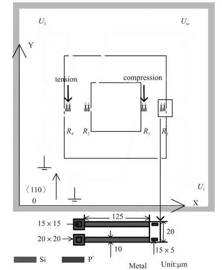
Fig.1 Layout of sensor chip structure
The sensitivity of a piezoresistive pressure sensor is given by
Uinrepresents full scale input,PMrepresents maximum applied pressure and U(PM)is the corresponding output.To enhance the sensitivity,the only single variable—U(PM)should be studied.
Initially,R1=R3=R2=R4=R and thus the bridge output Uout=0.When pressure is exerted on surface of the chip,values of resistance change are approximately equal but have opposite signs and thus both types of piezoresistors can contribute to the bridge output.That is,ΔR1=ΔR4≈ΔR andΔR2=ΔR3≈-ΔR,which results in
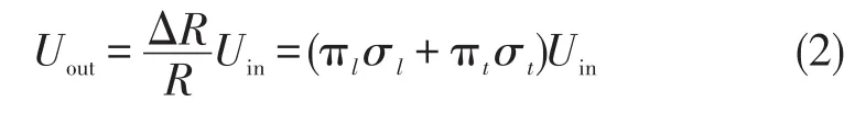
πlis longitudinal piezoresistive coefficient and πttransverse piezoresistive coefficient.σland σtare longitudinal stress[defined by Y in Fig.1]and transverse stress[defined by X in Fig.1]of the diaphragm,respectively.
From the equation(2),it is obvious that piezoresistive coefficients and stresses values are contributed to influence factor of the sensitivity.The piezoresistive coefficients are mainly connected to resistance material including crystal orientation and doping concentration[5],and the values of stresses are related to the chip structure and its shape.
To obtain the highest sensitivity,p-type singlecrystal SOI wafer is selected as piezoresistor material and four piezoresistors are arranged along<110>orientation.From both sensitivity and productivity considerations,the favored sensor chip shape is square[6-7].A surface impurity concentration of 3×1018cm-3is chosen to reduce temperature sensitivity of piezoresistors and maintain a high piezoresistive coefficients[5].
In〈110〉direction,Uoutcan be described as
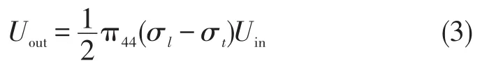
Therefore,Uoutis proportional to differential stress(σl-σt)and sensitivity improvement of SOI pressure sensor requires(σl-σt)to be maximized.When a bossed diaphragm is used,difference effect of stresses and stiffness of the diaphragm can be enhanced[8].Thus relatively good sensitivity and better linearity can be achieved,which is critical for wide-pressure range.
3 Simulation and optimization of diaphragm structure
Since analytical theory for calculating deformation and stress in the bossed diaphragm is complicated,ANSYS software is used for mechanical study of the chip structure.Dimensions for simulation is presented in Table 1.
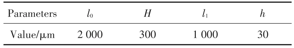
Table 1 Dimension of the structure
Mechanical simulation of SOI sensor is a silicononly model with Young’s modulus of 1.69×10¹¹Pa and Poisson’s ratio of 0.279,which for simplicity and speed of simulation.Clamping boundary is defined at bottom area of the structure.The simplified model is reasonable because the Young’s modulus of thin SiO2layer is low enough that its effect can be lumped in the silicon[9].When higher pressure is exerted,the deflection of diaphragm may become nonlinear.Therefore,nonlinear simulation in ANSYS is necessary to guarantee feasibility of the design.Further simplification here also neglects depth of the piezoresistive regions.
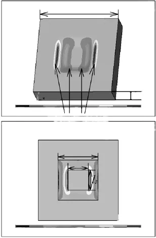
Fig.2 Stress distribution on the sensor chip for an applied pressure of 10 MPa
Fig.2 shows stress distribution of the sensor chip for an applied pressure of 10 MPa with a 500 μm×500 μm×470 μm(l2×l3×h)boss.When the pressure rises to 10 MPa,maximum stress on the sensor chip is about 2120 MPa,which is less than the tensile ultimate stress of silicon rupture stress(7 000 MPa).Hence the diaphragm would not be fractured under the pressure of 10 MPa.Maximum(σl-σt)can be found at positions of x1=520 μm,x2=736 μm,x3=1264 μm and x4=1480 μm by path simulation,which are not exactly at the edges of clamping support and boss.To achieve high sensitivity,four piezoresistive elements should be placed in these four points separately.
The boss thickness and shape are also related to the sensor sensitivity and the overload capacity.Large boss will function as mobile mass of an accelerometer,which will increase additional acceleration sensitivity and eventually influence stability of diaphragm unpredictably[10].To reduce difficulty and complexity of the measurement,the boss should be as thinner as possible.Fig.3 indicates that the less the thickness is,the more excellent sensitivity the chip will achieve.When nonlinear analysis of ANSYS has been taken into account,the chip with the boss thickness of only 25 μm can still guarantee a good linearity in the range of 10 MPa while that the center deflection of flat diaphragm changes nonlinearly.In addition,the linearity of the chip doesn’t be impaired apparently when overload pressures of 10 MPa to 20 MPa are applied.Therefore,a shallow-boss sensor structure can be loaded to wide range measurement for outstanding linearity,better sensitivity and proper overload pressure of at least 20 MPa.

Fig.3 Change of center deflection with different boss thicknesses
The boss shape depends on different aspect(l2/l3)ratios.Fig.4 shows how maximum differential stress values change when different aspect ratios of boss are applied.The thickness of the diaphragm is fixed as 180 μm.It is clear that the ranges of maximum(σl-σt)values are in the linear region for all kinds of boss aspect ratios.Tensile stresses can be increased proportionally with the decrease of aspect ratios.On the contrary,compressive stresses become almost the same since aspect ratios of boss reduce to 0.8.This means that the absolute stress values of tension and compression are no longer the same.A favored ratio should be 1(square shape)for equality of two kinds of stresses.
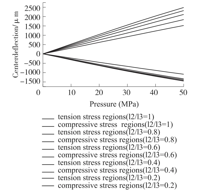
Fig.4 Change of maximum differential stress values with different aspect(l3/l2)ratios of boss
4 Design of piezoresistors and metal wires with high-temperature consideration
Not only doping concentration affect piezoresistors performance at high-temperature environment,but also heat generated by piezoresistors.To minimize the heat production,power consumption of piezoresistors should be small so that width of piezoresistors should be as broad as possible.Excitation voltage of the bridge is assumed 5 V and thus the original value for each piezoresistive element is 2.5 kΩ.
For the objective of high sensitivity,two pairs of piezoresistors are supposed to centralize in the regions of maximum difference of stresses as shown in Fig.1.Thus the width of piezoresistors should be thin since those high stress difference areas are narrow and focused.What’s more,longer and narrower the piezoresistor,larger the resistance will be obtained and current flow of piezoresistor will be one dimensional.An optimal ratio between the length and width of the piezoresistor should be ten[11].After detailed consideration and weighing up the dimension,resistance and sensitivity,the width and length of the piezoresistor were decided to be 10 μm and 250 μm with Rs=100 Ω/口.To keep both high uniformity and sensitivity,piezoresistor with 2 turns(U shape)is more suitable than with 1 turn(straight shape).This is because that piezoresistors can be avoided to extend to areas of low stresses difference when utilizing U shape.
On the other hand,alignment of bossed structure photolithography and verticality during deep etching process always have deviation,so edge-offset is inevitable.Since the stresses are non-uniform and rapidly changing in maximum(σl-σt)locations,the location change of diaphragm edges will affect force situation of piezoresistors,which will influence the achievement of highest sensitivity in the end.U-shaped piezoresistor pattern can compensate this kind of edge-offset.Each piezoresistor is placed symmetrically cross its corresponding x-axis value,connected by multi metal with a space of 20 μm,so that the impact of edge-offset can be reduced greatly.The value of space should be small for the purpose of sensitivity,determining by maximum possible alignment error(±2 μm)and etching verticality error(±2°)in our laboratory,as Fig.1 plots.In addition,the doping uniformity of the centralized piezoresistors is better than piezoresistors diffused at the edge of the diaphragm,which can reduce output zero offset[1].
Metal wires will easily be oxidized and have larger resistance at high-temperature environments.Ti-Pt-Au layers are sputtered on the surface of chip to solve the problem of oxidization for their good stability at high-temperature environments.As for resistance value change,it can be weaken by differential wires arrangement[12].As Fig.1 illustrates,metal wires are placed symmetrically according to the diaphragm center with same size.Hence Equation(3)should be replaced by Equation(4),defined as
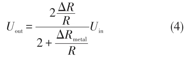
ΔRmetalis the resistance change of wire for each single piezoresistor.It is far less than 1 Ω/100 K,leading to slight influence for bridge output.
5 Results and discussions
Table 2 is a comparison between proposed sensor and other types of wide-range sensors that has been reported[13-14].It is obvious that the incorporation of shallow central bossed diaphragm with U-shaped piezoresistors can remarkably enhance sensitivity and overload capacity under wider range.Moreover,the optimized structure has an advantage of easy manufacture.From what has been discussed above,a SOI sensor of 10 MPa operation range with 180 μm boss thickness has been fabricated,as illustrated in Fig.5.
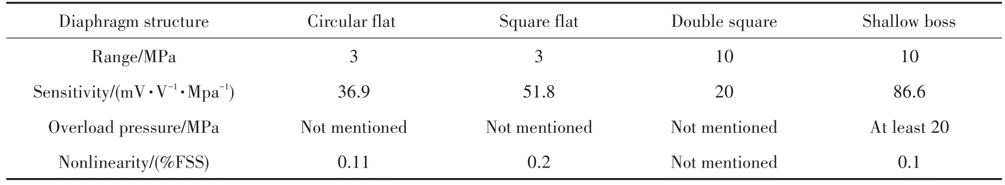
Table 2 Performance comparison with other types of wide-range sensors
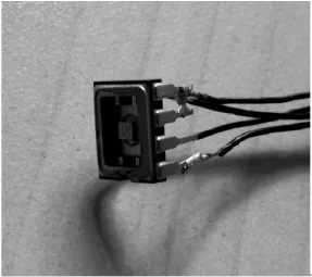
Fig.5 Practical view of the fabricated pressure sensor
6 Conclusions
In this paper a high sensitivity piezoresistive SOI pressure sensors for 10 MPa range has been presented.The characteristic of the shallow square boss enables the optimum configuration to provide a wide measurement range with high sensitivity,excellent linearity and certain overload capacity through a series of ANSYS simulation.A centralized U-shaped piezoresistor design is an effective method to keep both sensitivity and uniformity of shallow bossed structure.High-temperature conditions is taken into account during the design procedure to satisfy high-temperature measurement request.By comparing with other types of widerange sensors that has been reported,it is concluded that the incorporation of shallow central bossed diaphragm with U-shaped piezoresistors could be an ideal candidate for wider-pressure and high-temperature sensing in real application.Based on the optimum design parameters,a piezoresistive SOI pressure sensor for wide measurement range has been successfully manufactured.Future work will be towards high-temperature testing of the proposed sensor.
[1]Niu Zhe,Zhao Yulong,Tian Bian.Design Optimization of High Pressure and High Temperature Piezoresistive Pressure Sensor for High Sensitivity[J].Review of Scientific Instruments,2014,85:1-8.
[2]GREGORY T A KOVACS.Micromachined Transducers Sourcebook[M].USA McGraw-Hill Companies Inc,1997:182-183.
[3]Zang Shuyu,Zang Weilian,Suo Kainan,et al.Research of SOI High Temperature Pressure Sensor[J].Chinese Journal of Sensors and Actuators,2006,19(4):984-987.
[4]Ni Zhiqi,Yan Suying,Zhang Shengcai.Simulation&Optimal Design of SOI Single-Crystal Silicon Pressure Sensor[J].Chinese Journal of Sensors and Actuators,2003,16(1):92-95.
[5]Tufte O N,Chapman P W,Donald Long.Silicon Diffused-Element Piezoresistive Diaphragms[J].Journal of Applied Physics,1962,33(11):3322-3327.
[6]Liu Zhenni,Tan Xiaolan,Yang Junsong.Research on a Micro Piezoresistive Pressure Sensor[J].Machinery Design&Manufacture,2012,1:103-105.
[7]Shen Siguo,Ding jianning,Pan Haibin,et al.Design and Performance Study on Nano-Silicon Thin-Film Ultraminiatured Pressure Sensor[J].Transducer and Microsystem Technologies,2010,29 (10):62-64.
[8]Li Sainan,Liang Ting,Wang Wei,et al.A novel SOI Pressure Sensor for High Temperature Application[J].Journal of Semiconductors,2015,36(1):014014-1-014014-5.
[9]Hermann Sandmaier,Karl Kuhl.A Square-Diaphragm Piezoresistive Pressure Sensor with a Rectangular Central Boss for Low-Pressure Ranges[J].IEEE Transactions on Electron Devices,1993,40(10):1754-1759.
[10]Ralph H Johnson,Said Karbassl,Uppill Sndhar,et al.A High-sensitivity Ribbed and Bossed Pressure Transducer[J].Sensors and Actuators A,1992,35:93-99.
[11]Huang Xian,Zhang Dacheng.A High Sensitivity and High Linearity Pressure Sensor Based on a Peninsula-Structured Diaphragm for Low-Pressure Ranges[J].Sensors and Actuators A,2014,216:176-189.
[12]Ranjith Amara,Dzung Viet Dao,Toshiyuki Toriyama,et al.Simulation,Fabrication and Characterization of a Three-Axis Piezoresistive Accelerometer[J].Smart Materials and Structures,2006,15:1691-1699.
[13]Wang Wei.Design and Fabrication of SOI High Temperature Pressure Sensor[D].Taiyuan,North University of China,2014.
[14]Santosh Kumar S,Pant B D.Design of Piezoresistive MEMS Absolute Pressure Sensor[C]//16th International Workshop on Physics of Semiconductor Devices,2011,8549:1-10.
[15]Suja K J,Vidya Gopal,Rama Komaragiri.Optimized Design of a Silicon Based MEMS Pressure Sensor for Wider Range and Better Sensitivity[C]//International Conference on Microelectronics,Communication and Renewable Energy,2013:1-5.

张 瑞(1990-),女,山西太原人,硕士研究生,研究方向为高温压力传感器,15135088678@163.com;

梁 庭(1979-),男,山西长治人,副教授、硕士生导师、博士,研究方向为高温压力传感器、MEMS器件及工艺,liangtingnuc@163.com。
一种大量程SOI压阻式压力传感器*
张 瑞1,2,梁 庭1,2*,熊继军1,2,刘雨涛1,2,王涛龙1,2,王心心1,2
(1.中北大学仪器科学与动态测试教育部重点实验室,太原030051;2.中北大学电子测试技术国防科技重点实验室,太原030051)
对传统的SOI压阻式压力传感器进行了结构优化。目的是提高灵敏度,以满足在高温环境下大量程压力测量的实际需求。通过力学性能模拟,采用浅凸台结构来提高灵敏度和测量范围。分析并模拟了凸台厚度和形状对灵敏度的影响。得到了适合高温工作的掺杂浓度,压敏电阻的尺寸,金属引线的材料和布局。电阻放置在(σl-σt)最大的区域以保持灵敏度和线性度。采用U形电阻补偿在浅凸台制作过程中的工艺偏差对灵敏度的影响。有限元分析(FEA)表明,优化后的芯片结构可以测量10 MPa范围内的压力,灵敏度高达86.6 mV/(V·MPa),非线性误差在0.1%以下。和其他文献报道的大量程压力传感器相比,浅凸台芯片结构灵敏度和过载能力优异。
大量程;SOI压阻式压力传感器;高温;有限元分析(FEA)
TP212
A
1004-1699(2015)08-1125-06
2015-04-20 修改日期:2015-06-08
��7230
10.3969/j.issn.1004-1699.2015.08.005
项目来源:The project is funded by the National Science Foundation for Distinguished Young Scholars of China(51425505);National Natural Science Foundation of China(51405454)
