Ultraviolet Photodetector based on Sr2Nb3O10 Perovskite Nanosheets
2024-04-11ZHANGBinbinJIAMengmengLIANGQiWUJinsongZHAIJunyiLIBaowen
ZHANG Binbin ,JIA Mengmeng ,LIANG Qi ,WU Jinsong ,ZHAI Junyi ,LI Baowen,*
(1.School of Materials Science and Engineering,Wuhan University of Technology,Wuhan 430070,China;2.CAS Center for Excellence in Nanoscience,Beijing Institute of Nanoenergy and Nanosystems,Chinese Academy of Sciences,Beijin 100083,China;3.State Key Laboratory of Advanced Technology for Materials Synthesis and Processing,Wuhan University of Technology,Wuhan 430070,China)
Abstract: Liquid-phase exfoliation was employed to synthesize Sr2Nb3O10 perovskite nanosheets with thicknesses down to 1.76 nm.Transmission electron microscopy (TEM),atomic force microscope (AFM),X-ray photoelectron spectrometer (XPS),and other characterization techniques were used to evaluate the atomic structure and chemical composition of the exfoliated nanosheets.A UV photodetector based on individual Sr2Nb3O10 nanosheets was prepared to demonstrate the application of an ultraviolet (UV) photodetector.The UV photodetector exhibited outstanding photocurrent and responsivity with a responsivity of 3 × 10⁵ A·W-1 at 5 V bias under 280 nm illumination,a photocurrent of 60 nA,and an on/off ratio of 3 × 10².
Key words: perovskite nanosheets;liquid-phase exfoliation;ultraviolet photodetector
1 Introduction
UV photodetectors have promising applications in deep space exploration,military detection,biological analysis,and optoelectronic neural networks due to their high energy,short wavelength,intense penetration,small spot limit size,and high-resolution imaging[1-4].Traditional photoelectric materials,such as silicon-based materials,GaAs,and ZnO,have been investigated for decades[5-8].However,they can not meet the requirements of electronic devices with miniaturization,integration,and flexibility[9,10].Therefore,it is of great importance for promising candidates to explore new materials.Recently,2D perovskites have attracted considerable attention for optoelectronic applications[11-13].However,some perovskites are unstable in the environment,and some have a toxic Pb element[14].So,seeking novel perovskite nanosheets is crucial for developing UV photodetectors.
Layered perovskite materials have exhibited excellent photocatalytic activity[15],ferroelectricity[16],high-temperature superconductivity[17],and giant magnetoresistance[18]because of the oxygen octahedron torsion and cation displacement[19].Layered perovskites mainly have three types,namely,the Dion-Jacobson(DJ) phase,the Ruddlesden-Popper (RP) phase,and the Aurivillius (AV) phase.The general formula of the structure of the DJ phase is A'[Am-1BmO3m+1](A' is an alkali metal,A is an alkali earth metal or bismuth lanthanum element,B is transition metal,andmis the thickness of perovskite layer).Importantly,DJ-layered perovskites can be exfoliated into monolayer nanosheets by liquid-phase exfoliation[20].Chemically exfoliated nanosheets have excellent electrical,optical,and electrochemical properties compared with their precursors.For example,Sr2Nb3O10perovskite nanosheets can be obtained by chemical exfoliation from its precursor KSr2Nb3O10.Sr2Nb3O10nanosheets have excellent photocatalytic activity[21,22]and dielectric properties[23],which do not contain toxic elements,are prepared and are stable at room temperature.Moreover,Sr2Nb3O10perovskite nanosheets have a wide band gap corresponding with the ultraviolet photon energy range for optical detection applications.
In this work,we prepared Sr2Nb3O10perovskite nanosheets with a thickness of 1.76 nm by liquid-phase exfoliation.X-ray diffraction (XRD),scanning electron microscopy (SEM),atomic force microscopy(AFM),transmission electron microscopy (TEM),and other characterization methods were employed to examine their structural properties.Finally,we fabricated the UV photodetector based on Sr2Nb3O10perovskite nanosheets.The UV photodetector exhibited outstanding photocurrent and responsivity with a responsivity of 3 × 10⁵A·W-1at 5 V bias under 280 nm illumination,a photocurrent of 60 nA,and an on/off ratio of 3 × 10².
2 Experimental
2.1 Materials
K2CO3(99.0%),SrCO3(99.995%),and Nb2O5(99.99%) were all purchased from Sigma Aldrich.The tetrabutylammonium hydroxide (TBAOH) and nitric acid solution were obtained from Sigma Aldrich and Sinopharm.
2.2 Synthesis of Sr2Nb3O10 perovskite nanosheets
KSr2Nb3O10powders were prepared by a solid-state reaction.Raw powders of K2CO3,SrCO3,and Nb2O5with the molar ratio of K: Sr: Nb=1.05: 2: 3 were mixed thoroughly by grinding the mixture for one h,then calcinated at 900 ℃ for one h in air.After the second grinding,the calcined powders sintered at 1 100-1 300 ℃ for 12 h in air.After two-step sintering,KSr2Nb3O10powders were stirred at 110 rpm in 5M HNO3,and HSr2Nb3O10·nH2O powders were obtained after natural drying.HSr2Nb3O10·nH2O powders were dispersed in an aqueous solution containing an equimolar amount of TBAOH.The Sr2Nb3O10nanosheets were obtained by shaking the TBAOH-containing solution under ambient conditions.
2.3 UV photodetector fabrication
For the fabrication of individual Sr2Nb3O10nanosheet photodetector,source/drain electrodes were patterned by standard electron beam lithography,including electron beam deposition of Cr/Au (10/50 nm)contacts and subsequent lift-off process.The devices were constructed by electron beam deposition of Cr/Au contacts,which were patterned by a shadow mask.
2.4 Characterization
The crystal structure of powders was obtained by X-ray diffractometer (SmartLab,Rigaku).The morphology of powder samples was evaluated by scanning electron microscope (JSM-7610FPlus).The elemental content ratio of the sample was measured by ICP atomic emission spectrophotometry (Prodigy 7) and K+content through atomic absorption spectrophotometry(CONTRAA-700).The surface morphology and thickness of perovskite nanosheets were characterized by an atomic force microscope (Asylum Research Cypher ES,Oxford).The chemical elements of nanosheets were obtained by an X-ray photoelectron spectrometer (XPS,ESCALAB 250Xi).The UV absorption spectra of the nanosheets were collected by UV/VIS/NIR Spectrometer (Lambda 750 S).The Raman spectra of samples were carried out using RENISHAW Raman microscope(InVia).Atomic structures were examined by a Double spherical aberration-corrected transmission electron microscope (Titan Cubed Themis G2 300).
A 450 W Xenon arc lamp facilitated with a monochromator was utilized as the light source,and the power density was measured with a power meter(PM100D).All the electric properties were conducted by a semiconductor characterization system (Keithley 4200,USA) and a probe station under the ambient environment.
3 Results and discussion
3.1 Synthesis and characterization of KSr2Nb3O10 and HSr2Nb3O10·nH2O
The precursor KSr2Nb3O10was prepared by solid-state reaction.We explored the optimal sintering conditions.First,the raw materials were mixed evenly and calcined at 900 ℃ for one hour.The calcined samples were then sintered at various temperatures for 12 h (see details in the Experimental Section).As shown in Fig.1(a),the samples sintered at 1 100,1 150,1 200,1 250,and 1 300 ℃ were analyzed by XRD.The FWHMs of the samples prepared at different sintering temperatures were about 0.1°,indicating that the prepared samples had high crystal quality.However,at an inappropriate sintering temperature,the prepared samples appear heterogeneous.For example,when the sintering temperature was 1 100 ℃,three impurity phases of SrNbO6,Sr2Nb2O7,and Sr6Nb10O30appeared.When the sintering temperature was increased from 1 150 to 1 300 ℃,the Sr2Nb2O7impurity phase also appeared.When the sintering temperature was 1 200 ℃,the sample was pure KSr2Nb3O10phase.Thus,the optimum sintering temperature for synthesizing precursor KSr2Nb3O10was 1 200 ℃.XRD patterns of the samples sintered at 1 200 ℃ show firm peaks at 5.9°,11.8°,32.5°,and 46.5°,corresponding to the (002),(004),(221),and (400)planes of KSr2Nb3O10,respectively.During the sintering process,K2O will affect the reaction due to evaporation,so excessive K2CO3is needed[23].Different excesses of K2CO3were added for exploration of the sintering conditions.XRD patterns of the samples are shown in Fig.1(b).When K2CO3is insufficient,KSr2Nb5O15and Sr2Nb2O7impurity phases will appear.However,when an excess of 5% of K2CO3and above were used,the samples were pure phase KSr2Nb3O10.In summary,the optimum sintering conditions are 1200℃ sintering temperature and 5% excess K2CO3.

Fig.1 (a) XRD patterns of KSr2Nb3O10 powders prepared at various temperatures;(b) XRD patterns of KSr2Nb3O10 powders prepared with different excess K2CO3
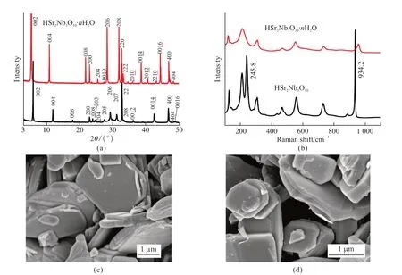
KSr2Nb3O10powders were mixed with nitric acid for an ion exchange reaction,and therefore,the proton phase HSr2Nb3O10·nH2O powders were obtained.A comparison of XRD patterns of KSr2Nb3O10and HSr2Nb3O10·nH2O powders is shown in Fig.2(a).As indicated in Fig.2(b),the strong peaks appearing at 5.4°,10.6°,28.1°,and 31.6° match well with the (002),(004),(206),and (208) planes of HSr2Nb3O10,respectively,indicative of the complete ion exchange.The precursor KSr2Nb3O10and the proton phase HSr2Nb3O10were further characterized by Raman spectroscopy.The Raman displacement from 100 to 300 cm-1represents the transverse vibration of K+ions and Nb5+ions.For example,the peak at 245.8 cm-1indicated the transverse vibration of K+ions (Fig.2(b)).After ion exchange,the disappearance of the peak at 245.8 cm-1indicates that the K+was replaced after ion exchange.Fig.2(c) and 2(d)show SEM images of KSr2Nb3O10and HSr2Nb3O10·n-H2O powders,respectively.The HSr2Nb3O10·nH2O powder maintains similar morphologies and sizes to the KSr2Nb3O10powders.

Fig.2 (a) XRD patterns of KSr2Nb3O10 and HSr2Nb3O10·nH2O powders;(b) Raman spectra of KSr2Nb3O10 and HSr2Nb3O10·nH2O;SEM images of (c) KSr2Nb3O10 and (d) HSr2Nb3O10·nH2O powders
3.2 Synthesis and characterization of Sr2Nb3O10 nanosheets
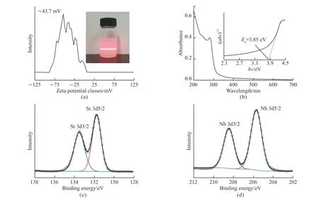
The protonic phase HSr2Nb3O10·nH2O powder was mixed with TBAOH solution at an equal molar ratio.The Zeta potential was tested to prove the stability of Sr2Nb3O10nanosheets in ultrapure water.Fig.3(a) shows that the average Zeta potential of Sr2Nb3O10nanosheets in ultrapure water was about -43.7 mV,suggesting that Sr2Nb3O10nanosheets have large electronegativity.The strong electrostatic repulsion between the Sr2Nb3O10nanosheets enables good dispersion in ultrapure water.The inset shows the optical photographs of colloidal suspensions of Sr2Nb3O10nanosheets.The Tyndall effect can be observed by laser irradiation.The optical band gap of Sr2Nb3O10nanosheets can be obtained by UV absorption spectroscopy.As shown in Fig.3(b),there are apparent absorption peaks at about 300 nm.The Tauc figure can be received by calculation,and the optical band gap is 3.85 eV.Figs.3(c)-3(d) show the elemental composition and chemical state of Sr2Nb3O10nanosheets characterized by X-ray photoelectron spectroscopy (XPS).The characteristic peaks of main elements of Sr and Nb can be measured by XPS.Two peaks centered at 133.5 and 131.8 eV in Fig.3(c) represent Sr 3d3/2and Sr 3d5/2,respectively.Two peaks at 208.5 and 205.7 eV in Fig.3(d) represented Nb 3d3/2and Nb 3d5/2,which confirmed that the valence states of Sr and Nb are +2 and +5,respectively.

Fig.3 (a) Zeta potential distribution of Sr2Nb3O10 nanosheets,inset shows the optical photograph of colloidal suspension of Sr2Nb3O10 nanosheets;(b) UV-Vis absorption spectra of diluted colloidal suspensions of Sr2Nb3O10 nanosheets;The inset shows the Tauc curve of Sr2Nb3O10 nanosheets.XPS spectra of (c) Sr 3d and (d) Nb 3d of Sr2Nb3O10 nanosheets
To determine the content ratio of each element,all samples were characterized by an inductively coupled plasma emission spectrometer (ICP).As shown in Table 1,the elemental ratio of the sintered precursor K: Sr:Nb=0.9: 2.1: 3.0,very close to the ideal ratio of 1: 2:3.After ion exchange,the elemental ratio Sr: Nb was 1.8: 3.0,slightly different from the perfect ratio of 2: 3.There was also a small amount of K+ions in the sample,which may be not cleaned when washed.The elemental ratio Sr: Nb of exfoliated nanosheets was 2.2:3.0.

Table 1 Elemental analysis results for layered perovskites,acid-exchange phases,and nanosheets/wt% (atomic ratio)
AFM and TEM were performed further to investigate the thickness and microstructure of the Sr2Nb3O10nanosheets.The nanosheets were transferred to the Si wafer by Langmuir-Blodgett (LB) method and characterized by AFM.It can be seen from Fig.4(a) that the thickness of the nanosheets was about 1.76 nm,which is consistent with previous reports[24].Fig.4(b) shows the nanosheets under low magnification transmission electron microscopy (TEM).Fig.4(c) is a high-resolution TEM image of the nanosheets,in which two vertical crystal planes with an interplanar spacing of 0.404 nm corresponded to (010) and (100) crystal planes of Sr2Nb3O10nanosheets.The precise atomic arrangement and no apparent defects can be seen in Fig.4(c),proving that the nanosheets have high quality.According to the electron diffraction pattern of Fig.4(d),the synthesized nanosheets are single crystals.

Fig.4 (a) AFM image of Sr2Nb3O10 nanosheets deposited on a Si wafer;the inset is the height profile of an individual nanosheet;(b) TEM,(c) HRTEM,and (d) selected-area electron diffraction pattern taken along the [001]zone axis of Sr2Nb3O10 nanosheets
3.3 Photodetecting performance of the individual Sr2Nb3O10 nanosheet
The schematic diagram of the photodetector based on an individual Sr2Nb3O10nanosheet is presented in Fig.5(a).Fig.5(b) shows the current-voltage (I-V) features of individual Sr2Nb3O10nanosheet photodetectors in a logarithmic plot in the dark and under light irradiation with different wavelengths.The dark current of 1 pA was significantly enhanced to 4 091 nA at 5 V at 280 nm.Fig.5(c) shows the photocurrent response characteristics of the device with 280 nm light under different bias voltages.The device's current-time (I-t) curves exhibited excellent reproducibility and stability.Under the bias voltage of 0.1,0.5,and 1.0 V,the photocurrents increased to 60,293,and 459 nA and decreased to 0.2,9,and 19 nA,respectively,with the 280 nm UV light turned on and off.The photodetector exhibited an on/off ratio of over 102 and a stable photocurrent of ≈60 nA at 0.1 V to incident UV light.Spectral responsivity (Rλ) and external quantum efficiency (EQE) are two critical parameters that can be used to evaluate the photoelectric performance of the individual Sr2Nb3O10nanosheet photodetector.These two parameters can be calculated according to the following equations:

Fig.5 Photodetecting performance of the individual Sr2Nb3O10 nanosheet: (a) Schematic diagram of a Sr2Nb3O10 photodetector;(b) I-V curves of the device under dark and UV illumination;(c) I-t curves of on/off switching at different bias voltages;(d) I-V curves for the device under various incident light densities
where,IdandIphare the dark and photocurrent,Pλis the incident power density,Sis the effective exposure area,andh,c,e,andλare the Planck’s constant,the velocity of light,the elementary charge,and incident wavelength,respectively.According to the equations and Fig.5(b),the individual Sr2Nb3O10nanosheet photodetector exhibited excellent UV photodetector performance under 280 nm light (1.20 mW·cm-2) at 5 V bias with a responsivity of 3×10⁵A·W-1and a high EQE of 2×10⁷%.Fig.5(d) exhibits theI-Vcharacteristics of the Sr2Nb3O10nanosheet photodetector under 280 nm illumination with various incident power densities.When the power density of the light illumination was increased from 0 to 1.417 mW·cm-2,the corresponding photocurrent increased current from 4.3×10³to 2.2×10⁴nA.These results suggest that the Sr2Nb3O10nanosheets have excellent sensitivity to UV light and outstanding UV photodetecting performance,which proves the broad applications of two-dimensional perovskite nanosheets in optoelectronic devices.
4 Conclusions
In summary,we optimized the synthesis process of precursor KSr2Nb3O10.Subsequently,single crystal perovskite nanosheets of Sr2Nb3O10were successfully prepared by liquid-phase exfoliation.The Sr2Nb3O10nanosheet photodetector exhibited outstanding photocurrent and responsivity with a responsivity of 3 ×10⁵A·W-1at 5 V bias under 280 nm illumination,a photocurrent of 60 nA and an on/off ratio of 3 × 10².This work demonstrates the potential of Sr2Nb3O10nanosheets for application in optoelectronic devices.
Conflict of interest
All authors declare that there are no competing interests.
杂志排行
Journal of Wuhan University of Technology(Materials Science Edition)的其它文章
- Biotin-modified Galactosylated Chitosan-gene Carrier in Hepatoma Cells Targeting Delivery
- Mussel-inspired Methacrylic Gelatin-dopamine/Ag Nanoparticles/Graphene Oxide Hydrogels with Improved Adhesive and Antibacterial Properties for Applications as Wound Dressings
- Effect of Polyvinyl Alcohol in Inner Aqueous Phase on Stability of Millimeter-scale Capsules
- Synthesis and Characterization of Nonionic Waterborne Polyurethane and Application to Wool Fabric Finishing
- Fluorescent Double Network Hydrogels with Ionic Responsiveness and High Mechanical Properties for Visual Detection
- Damage Mechanism of Ultra-thin Asphalt Overlay (UTAO)based on Discrete Element Method
