A hybrid chemical modification strategy for monocrystalline silicon micro-grinding:Experimental investigation and synergistic mechanism
2023-09-05YinghuiRENKexinLIWeiLIXingmingHUANGXiomnLIUGenyuCHENToshiroDOI
Yinghui REN, Kexin LI, Wei LI, Xingming HUANG, Xiomn LIU,Genyu CHEN, Toshiro DOI
a College of Mechanical and Vehicle Engineering, Hunan University, Changsha 410082, China
b Laser Research Institute, Hunan University, Changsha 410082, China
c Kyushu University, Fukuoka 814-0001, Japan
KEYWORDS Modification strategy;Monocrystalline silicon;Multi-energy fields;Selective surface modification
Abstract For high performance manufacturing of micro parts and features, a hybrid chemical modification strategy is proposed to decrease critical energy barrier of mechanical removal of hard and brittle crystal material by refining localized machining condition.The strategy, namely UVlight and IR-laser hybrid chemical modification(UVIR-CM)strategy,includes two steps,an ultraviolet light(UV-light)catalytic advanced oxidation and an infrared laser(IR-laser)assisted selective modification based on Fenton liquid–solid reaction for monocrystalline silicon.The modification effects of UVIR-CM strategy were investigated by surface morphology micro-observation, crosssection transmission electron microscopy (TEM) observation, Raman spectroscopy analysis and nanoindentation test.Experimental results demonstrated that varied degrees of laser texturing appeared on different strategy samples’IR-laser scanned area.And the IR-laser thermal damage has been successfully inhibited due to the refraction and reflection of energy by bubbles in liquid medium.But for the UVIR-CM strategy, a uniform and amorphous silicate layer is detected in a certain boundary.The UV-light promotes oxidation cycle ability of the chemical solution and ensures sufficient oxide modified layer for subsequent step.Attributing to synergism of photochemical,photothermal and kinetic effects induced by IR-laser,the modified layer displays layered structure with about 600 nm thickness, (2.7 ± 0.60) GPa nanohardness, and (93.7 ± 22.9) GPa indentation modulus.And the layered structure is amorphous layer, nanocrystal and micro-twins layer from the surface to the interior of sample.Consequently, it reveals that the subsequent mechanical removal will become easy due to decreasing energy barrier of monocrystalline silicon in selective area.Meanwhile, its original excellent mechanical properties also are maintained under a certain depth.The results contribute to develop a novel combined micro-machining technology to achieve collaborative manufacturing of structure shape and surface integrity for micro parts and feature.
1.Introduction
For several decades, the dramatically increasing demand of micro parts and features, such as micro-grooves, microchannels and micro-lens array for drag reduction function surface or heat exchanger devices or imagine formation devices in aerospace field, optics field, and so on, has aroused researchers’strong interests to explore novel high performance micro-machining technologies.1,2Micro-grinding with micro pencil grinding tool (tool diameter ∅<1 mm) is an effective and available emerging technology for manufacturing micro parts and features of hard and brittle crystal materials.1While its process capability reaches limit and is hard to fulfill ideas of manufactures, whose processing quality is easily influenced by material property, tool geometry and tool wear.3,4For example,edge crack propagation or fracture of micro parts and features is still a concern for hard and brittle crystal materials micro-grinding.5–7Under size effect, the faint mechanical removal energy of micro-scale tool is difficult to break critical energy barrier of hard and brittle crystal material and reaches damage free surface though the tool operates in high level(spindle speed > 50000 r/min).8Therefore, the tool is quickly worn to affect shape precision of micro parts and features.1,9Guo et al.10expounded that if want to achieve high performance manufacturing of both properties and geometries, processing loads,such as mechanical,thermal,chemical nature or combination of them,should be active determined with energy input conditions.Therefore, how to control energy input conditions and break critical energy barrier becomes a challenge for micro parts and features micro-grinding of hard and brittle material.
Numerous works have been conducted to decrease the critical energy barriers of hard and brittle material assisted by other energy field.The machining condition will been refined and the material machinability will been improved.Then better surface finish, lower tool wear and higher shape precision etc.have been obtained.Generally, chemical-assisted and laser-assisted processes have widespread applications to refine machining condition for hard and brittle material.It is wellknown that the chemical mechanical polishing (CMP) refines machining condition by alternating hybrid process of chemical reaction,and abrasive mechanical remove.11The CMP process can obtain nanoscale roughness and defect-free subsurface.While its material removal rate is extremely low.Researchers hope to reveal its chemical reaction mechanism and improve reaction efficiency and reaction degree.Zhou et al.12applied Fe nanoparticles in the polishing slurry to increase material removal rate for higher concentration of hydroxyl radical(*OH).Lu et al.13investigated the effects of Fe2+and H2O2concentration and pH of Fenton reagents on the chemical reaction rate of SiC wafer during CMP process.*OH produced in Fenton reaction induced the SiC surface to produce low-hardness SiO2, and the larger concentration of *OH promoted the polishing quality and enhanced the efficiency of CMP.Wang et al.14improved CMP performance in 4H-SiC substrate by combing mixed abrasive slurry and UV light photocatalytic effect.These works demonstrate that the liquid–solid chemical reaction and catalyst are crucial for the change degree of energy barrier during the chemical-assisted processes.The CMP is an excellent global planarization method widely applied in wafer manufacturing which also provide a reference for processing of hard and brittle material micro parts and feature.But optimal process condition is needed to obtain higher reaction efficiency and degree,especially in selective area to realize controllable liquid–solid chemical reaction.
Meanwhile, benefiting by selective and high energy characteristics, laser-assisted processing is also an effective way to refine machining condition for hard-to-cutting materials,especially for hard and brittle materials.Kumar et al.15presented laser-assisted micro-grinding to create three-dimension micro-features of ceramic.However, the laser-assisted microgrinding could obtain higher material removal rates, but thermal damage was difficult to eliminate.Madhukar et al.16employed a co-axial water-jet assisted fiber laser processing to fabricate micro-grooves.Attributing to high shear force of water-jet, molten materials around micro-groove were removed and the degree of thermal damage was controlled,while the recast and oxide layer at groove edges were still existed.Charee et al.17employed an ultrasonic assisted underwater laser processing to flush the debris, which efficiently reduced thermal damage and material deposition in cutting surface.Nonetheless, bubbles were generated by high ultrasonic frequency widened the micro-channels.The shock pressure generated by forming and collapsing of cavitation leaded to the production of micro-cracks in workpieces.Chemical-assisted laser processing also can improve machinability of hard and brittle crystal material.Kwon et al.18investigated a laser induced backside wet etching process to prevent micro-cracks in silicon and copper by adding phosphoric acid to the absorbent.The processable depth was increased to five times that of the absorbent without phosphoric acid, while the micro-cracks caused by laser at micro-channel bottom were not avoid.Wang et al.19prepared some micro-grooves on SiC surface by laser-chemical hybrid machining technology.They found that the exorbitant laser fluence produced mechanical spallation, which damaged the machined micro-structures.Ding et al.20proposed a laser-assisted machining hybrid post-etching method for the texturing of multi-crystalline silicon.The processing efficiency was increased by 19.26 % comparing with the standard acid textured ones.Thermal damage induced by laser can be controlled by water-assisted processing,but the accuracy loss of micro structure caused by bubbles in water is needed to pay close attention.However,there were still the laser ablation damages, which were not completely removed even after post-etching.The chemical-assisted laser processing can improve machinability of hard and brittle material, but the residual thermal damage and mechanical damage cannot be ignored.Therefore,how to effectively control energy input in the hybrid process, which signally affects damage degree and material machinability of micro parts and features,is a vital problem.
In this work, an ultraviolet light (UV-light) and infrared laser (IR-laser) hybrid chemical modification (UVIR-CM)strategy, which is a two-step controllable and selective surface modification process,is proposed to refine localized machining condition for monocrystalline silicon micro groove.The surface modification strategy combines the advantages of chemical-assisted process and laser-assisted process for hard and brittle material.To investigate the synergistic effects of UVIR-CM strategy on chemical modification efficiency and machinability of monocrystalline silicon, series of contrast experiments are carried out based on different chemical modification strategies.And reaction temperature, product,microstructure and mechanical properties are tested.It can provide a theoretical and experimental guidance for high performance micro-manufacturing of hard-to-cutting material in the future work.
2.Principle of UVIR-CM strategy
For global and local planarization of the wafer in integrated circuit manufacturing with CMP, the monocrystalline silicon was firstly oxidized by hydroxyl radicals(*OH)and then transformed into silicate based on liquid–solid chemical reaction Eqs.(1) and (2).21The removal of silicate layer by abrasive is easier than that of monocrystalline silicon.Inspired by monocrystalline silicon CMP process, we consider if the liquid–solid chemical modified reaction only occurs in selected area and implements comparatively precise control of reaction degree, it can make easier to obtain high quality microstructure in subsequent mechanical removal.22In order to solve these problems, controllable and stabilized chemical modification process is essential within selected microstructure area.According to Eqs.(1) and (2), the *OH and alkaline solution is necessary reaction condition for chemical modification of monocrystalline silicon.The hydrogen peroxide (H2O2) can create strong oxidizing *OH by Fenton reaction (Eq.(3)).It is well-known that chemical stability of H2O2is poor because it is easily dissolved into water (H2O)and oxygen (O2) under natural conditions.And the ferrous ion (Fe2+)transforms to the ferric ion (Fe3+) in Fenton reactions (Eq.(3)).Therefore, it needs to continuously supply the catalyst Fe2+and the oxidant H2O2to ensure sufficient strong oxidizing *OH.It results in a weak material removal rate for monocrystalline silicon CMP process because the modification reaction rate and degree are seriously restricted.
In order to improve reaction rate and accomplish controllable chemical modification in selected area, a UV-light and IR-laser hybrid modification (UVIR-CM) strategy is designed for monocrystalline silicon micro-groove.The UVIR-CM strategy is based on liquid–solid chemical reaction process that includes the UV-light advanced oxidation reaction step and IR-laser assisted selective chemical modification step.The principle sketch map of UVIR-CM strategy is shown in Fig.1.In the first step, the UV-light is introduced in the Fenton reaction between weak alkaline solution and monocrystalline silicon for a certain time, called UV-light catalytic advanced oxidation step.The advanced oxidation reactions are induced to produce an adequate oxide layer for next step.During the advanced oxidation step, H2O2decomposes into*OH by UV-light (Eq.(4)).Based on the UV-light catalytic advanced oxidation the *OH can be further produced in recycling(Eq.(5)and(6)).23Simultaneously,the Fe3+produced in Fenton reaction (Eq.(3)) is also retransformed to the catalyst Fe2+by UV-light (Eq.(7)).Attributing to UV-light photocatalysis the Fenton reaction can continuously proceed without adding additional Fenton reagents.Therefore, the recycling of*OH and Fe2+will significantly increase oxidation ability of the solution for the monocrystalline silicon liquid–solid reaction.
Traditional microscale subtractive manufacturing by micro-size diameter cutting tool, such as micro-grinding, can only output faint mechanical removal energy due to the size effect.It is difficult to break the critical energy barrier of hard and brittle material.The chemical modification process is accompanied with chemical bond destructing and reconstructing process that contributes to decrease the energy barrier of atoms layer removal.8According to Arrhenius equation,24the reaction rate and product concentration will be synchronously accelerated at high reaction temperature in a certain temperature range.Thus, to accelerate the liquid–solid reaction rate, the high energy field is a necessary condition.The new product and micro-defects should be induced towards the target of decreasing energy barrier.In the second step, the ultra-fast picosecond IR-laser has been performed to accomplish selective chemical modification, which is called as IRlaser assisted selective modification step.After finishing UVlight radiation, the sample is still immersed in the solution.The IR-laser scans sample following preset path within premachining area of micro-structure parts.The intensive energy of IR-laser transfers into heat and kinetic energy focused on sample’s surface and the solution around scanned spot area,so the reaction rate of Eq.(2) will be increased.Therefore,the controllable reaction degree and selective reaction area will be obtained.In other hand, we wish the silicates layer only produced in IR-laser scanned area due to the localized and selective high energy.It will contribute to decrease the energy barrier through generate lower hardness product in selected area for subsequent mechanical removal.

Fig.1 Sketch map for UVIR-CM strategy.
3.Experimental design
3.1.Experimental parameters
Series of experiments were carried out to verify feasibility of the UVIR-CM strategy and to explore influence factors of modification strategy, such as different modification steps and IR-laser scanning medium.The undoped (100) oriented monocrystalline silicon was selected as sample with dimensions of 15 mm × 10 mm × 3 mm.It was single-side polished with initial surface roughness Ra of 0.5 nm in advance.A fresh weakly alkaline modification solution, which mainly included H2O, H2O2, Na2CO3, C6H15NO3and EDTA-Fe-Na, was prepared with a pH of 10 and used timely at room temperature to ensure its chemical activity.22The experiment was performed according to the principle of UVIR-CM strategy.In the first step,an alumina crucible was selected as reaction vessel to hold samples and the solution to avoid interference of other reaction.All reaction vessels were irradiated for 10 mins by UVlights under a protection cover.The total radiation intensity of UV-light is 6822 μW/cm2.In the second step, a picosecond pulse infrared laser (PX200-1-GM, Edge Wave GmbH) was selected as IR-laser source with 1064 nm wavelength and 10 ps pulse width.The laser was installed on a CNC ultraprecision surface grinding machine (SL800A/1-HZ, Zhejiang Hangzhou Machine Tool Group CO., ltd) as shown in Fig.2.After UV-light irradiating, the reaction vessel was quickly transferred to machine table in order to avoid the solution failure in air.Then the IR-laser scanned samples line-byline at 0.05 m/s within preset rectangular area (0.7 mm × 8 m m)with 30 W average laser power.The laser spot diameter was 40 μm with a defocusing of + 163.5 μm.The laser pulse repetition frequency was 400 kHz.
Parameters and strategy conditions of contrast experiments are presented in Table 1.In IR-laser assisted modification in chemical solution (IR-CM) strategy, the sample was placed in reaction vessel with freshly solution and then subjected to IRlaser scanning.In UV-light and IR-laser coupling modification in deionized water(UVIR-DW)strategy,after UV-light catalytic advanced oxidation step, the oxidized samples and deionized water were put in reaction vessel and scanned by IR-laser.In UV-light and IR-laser coupling modification in air (UVIR-AR)strategy, the sample was scanned by IR-laser in air after UVlight catalytic advanced oxidation step.To ensure the consistency of IR-laser incident energy, the depths of liquids in the reaction vessel were 5 mm.The IR-laser scanning process was repeated five times for each sample under same strategy.Considering heat accumulation effect of IR-laser scanning, the reaction temperature field was real-time monitored by an infrared thermal imaging instrument (A615, FLIR Systems, Inc.).

Fig.2 IR-laser selective modification platform.

Table 1 Parameters for processing experimental samples.
3.2.Performance evaluation
The surface morphology of IR-laser scanning area was observed by scanning electron microscopy (SEM, Helios 5 CX,Thermo Fisher Scientific,Inc.)with tungsten(W)filament 5 HV.The micro-structure of cross-section of samples was observed by transmission electron microscopy (TEM, Titan G2,Thermo Fisher Scientific,Inc.).Fig.3 depicts the preparation procedure of the cross-sectional TEM foil.The crosssectional TEM foil was treated by focused ion beam (FIB)technique with different beam current (47nA, 2.5nA, 0.49nA,etc.) until the final dimensions was 10 μm × 6 μm × 80 nm.A platinum(Pt)coating was deposited over the sample to protect from the Ga+ion beam.
A confocal Raman microscope (Alpha 300R, WITec CO.,ltd) was applied to detect the reaction product on the IRlaser scanning area through analyzing Raman shift of characteristic peaks.The Raman intensity indicates that the Raman optical activity and content of vibration clusters.There are considerable errors between Raman intensity of different samples.So the Raman shift was only used to make a qualitative analysis of newly generated reaction products in this work.The analytical pure Na2SiO3and the undoped (100) oriented monocrystalline silicon (Si) were selected as check samples to compare with test samples.
To measure the fundamental mechanical properties of modified layer and evaluate modified degree of different strategy,nanoindentation was applied.Firstly, each sample was being indented in a series of indentations of 3 × 3 arrays on IRlaser scanned area using the MCT + UNHT Nano Hardness Tester (Swiss CSM Instruments Co., ltd.) by a Berkovich indenter.Each indentation process was performed in a loadcontrol mode.The loading/unloading rate and the maximum load were 10 mN/min and 5 mN, respectively.At the peak load, the indenter was held for 15 sec to avoid the influence of creep on unloading properties.Each indentation was separated by 10 μm to avoid any possible interference from the neighboring indents.The scan area of as 30×30 μm2was chosen to observe qualitatively all imprints of nanoindentation by the atomic force microscopy(AFM,NanoMan vS Multimode,Veeco Instruments, Inc.).The nanohardness and indentation modulus were calculated in Oliver and Pharr method.Furthermore, the deformation and fracture feature were investigated to evaluate modified degree based on a load–displacement curve of modified sample by a Berkovich indenter in a constant loading rate mode.The loading/unloading rate and the maximum load and holding time were 100 mN/min, 50 mN, and 15 sec, respectively.
4.Results
4.1.Reaction temperature field
Fig.4 shows different samples’reaction temperature field at same IR-laser scanning moment.The heat of laser spot radiated from inside to outside.The localized maximum temperature was marked by a red triangle label in Fig.4.In the liquid mediums, such as the chemical modified solution and deionized water, samples’maximum temperatures, which located around the IR-laser spot as shown in Fig.4(a)-4(c), were all below 90℃.The UVIR-CM sample’s maximum temperature was slightly higher than those of IR-CM and UVIR-DW samples.But in air medium, the UVIR-AR sample was entirely heated, and the maximum temperature reached 136.3℃, as shown in Fig.4(d).
The temperature variation curve and distribution feature of UVIR-CM sample was recorded in Fig.5.As IR-laser continuously scanned,the maximum temperature around spot region slowly increased from 61.4℃for the first scanning time to 81.6℃for the fifth scanning time.It’s worth noting that the temperature of reaction solution still exhibited relatively stable state.The minimum temperature of the UVIR-CM sample was below 43℃in different moments and the average temperature of reaction solution almost remained stable.
4.2.Modified surface morphology

Fig.3 SEM images for preparation procedure of cross-sectional TEM foil.
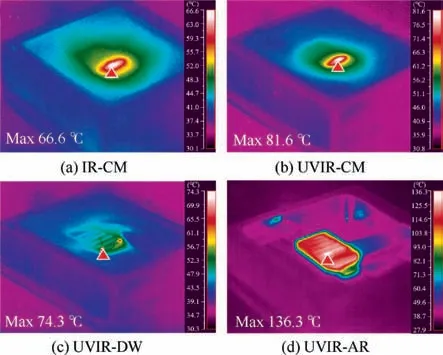
Fig.4 Infrared temperature field of samples under different modification strategies.

Fig.5 Reaction temperature curve and distribution field of UVIR-CM sample.
Fig.6 shows the morphology of samples under different modification strategies.There are obvious differences between the IR-laser scanned and unscanned area of all sample.The scanned area and unscanned area are named as modified area and unmodified area, respectively.There was a discontinuous boundary and some little smooth blocky spots in the IR-CM sample (Fig.6(a)).Some little spherical or short stick-like textures(length of about 296 nm to 730 nm)were exhibited in the modified area of IR-CM sample (Fig.6(a)).It presented relatively homogeneous morphology features in the modified area of the UVIR-CM sample (Fig.6(b)), and the loose long sticklike textures (length of about 1445 nm to 1598 nm) presented in short range order arrangement.Some large irregular smooth spots appeared in the modified area of UVIR-DW sample where the morphology feature was similar with that of the IR-CM sample (Fig.6(c)).In the modified area of UVIRDW sample, several little granular or long stick-like textures(length of about 585 nm to 730 nm)were also observed.Distinguished from non-continuous boundary of the IR-CM and UVIR-DW samples and rough boundary of the UVIR-CM sample, the UVIR-AR sample presented a straight boundary between the modified area and unmodified area as shown in Fig.6(d).There were distinct differences of morphology features representing laser melting characters.The heat affected zone (HAZ) of the UVIR-AR sample exhibited two kind of morphology marked in Fig.6(d).The HAZ I was narrow and adjoined with the boundary, while the HAZ II was wider and closed to the laser scanning center.In the HAZ I, there were a great deal of small size micro-holes and few craters.In the HAZ II, there were lots of varying sizes micro-cracks and micro-holes.The diameter of micro-holes increased sharply, and formed craters and thermal cracks gradually from the boundary to the laser scanning center.Obviously, the UVIR-AR sample suffered severe thermal damage.As indicated above, the morphology of modified area was significantly affected by modification step and IR-laser scanning mediums.
The bright field TEM image of UVIR-CM sample presented layer structure characteristic in the cross-section of scanned area as shown in Fig.7(a).Beneath the Pt coating,there was a certain thickness vitrified layer with light color in Fig.7(a).The thickness of vitrified layer ranged from 260 nm to 750 nm with average thickness of 447 nm.Some kink feature appeared beneath the vitrified layer with dark color, named kink feature layer.Its thickness fluctuated from 0 to 745 nm with average thickness of 210 nm.Beneath the kink feature layer, some bent-stripe feature can be observed on the bottom of cross-sectional TEM image.The bentstripe feature was further analyzed by the fast Fourier transform (FFT) analysis as shown in Fig.7(b).The FFT result confirmed that diffraction pattern of bent-stripe matched single-crystalline phase characteristic of monocrystalline silicon.The vitrified layer was further observed by high resolution(HR) TEM, which was marked by red solid box in Fig.7(a).And it presented atomic reordering morphology in Fig.7(c).The FFT results of Fig.7(c) presented a mixed pattern of amorphous diffused rings and single crystalline dots in Fig.7(d).It indicated that the vitrified layer contained both amorphous phase and crystals phase.The HR-TEM image of kink feature layer shown ordered and disordered two kinds of crystalline arrangements in Fig.7(e), which was marked by red dashed box in Fig.7(a).There were amorphous diffused rings and two sets of diffraction spots in Fig.7(f).Compared with Fig.7(b),it indicated that the brighter set of diffraction spots belonged to monocrystalline silicon and the other set of diffraction spots appeared at 1/3 of the diffraction spots of silicon in Fig.7(f).These two sets of diffraction spots confirmed that the micro-twins were formed in the kink feature layer.Therefore, amorphous phase and micro-twins were coexisted in the kink feature layer.The interface region between the vitrified and the kink feature layers(marked by red dotted box in Fig.7(a))had been further observed as shown in Fig.7(g)and(h).Some nanoparticles of around 5 nm size randomly dispersed in Fig.7(g), which possessed line lattices in different directions and line spacing.For example, the line spacing of the three nanoparticles (with two overlapping) was 7.6 A˚,7.8 A˚ and 8.5 A˚ in the Fig.7(g),respectively.Its FFT indicated that there were fresh nanocrystal particles in Fig.7(h).This was obviously different from the micro-twins and monocrystalline silicon.Based on above results, it can be inferred that the modified layer of UVIR-CM sample is consisted of vitrified layer and kink feature layer displayed amorphous phase,nanocrystal particles and micro-twins layer with average thickness of 600 nm.

Fig.6 SEM images for samples under different modification strategies.
4.3.Modified products
Fig.8 shows Raman spectra of samples under different modification strategies.At Raman shift of 510 cm-1and 952 cm-1,all samples’Raman spectra and Si check sample’s appeared similar characteristic peak.It indicates that monocrystalline silicon still existed in IR-laser scanned area of all samples.The UVIR-CM sample appeared distinct characteristic peaks at Raman shift of 300 cm-1and 614 cm-1, which related with amorphous silicon oxides.There were remarkable characteristic peaks at Raman shift of 129 cm-1,165 cm-1,370 cm-1and 782 cm-1in analytical pure Na2SiO3check sample.The Raman shift of UVIR-CM sample well matched with that of Na2SiO3check sample at Raman shift of 129 cm-1and 165 cm-1.And the characteristic peak of UVIR-CM sample at Raman shift of 355 cm-1presented a small amount of red-shift, which matched with the characteristic peak of the Na2SiO3check sample at Raman shift of 370 cm-1.The similar characteristic peak could not be found in other sample.It suggests that a certain number of silicates were formed on the UVIR-CM sample’s surface.While the UVIR-CM sample did not find the characteristic peak at Raman shift of 782 cm-1.It may be that there are different clusters of silicates between UVIR-CM sample and Na2SiO3sample.25Therefore,it can be inferred that some fresh silicates and amorphous silicon oxides generated on the IR-laser scanned area of UVIRCM sample.
4.4.Mechanical properties of modified area
Fig.9(a)shows the 3×3 nanoindentation array and test serial number of imprints on Si sample.The nanohardness and indentation modulus of all samples were described in Fig.9(b) and 9(c), respectively.These modified samples had lower nanohardness than that of Si sample (12.5 ± 0.5) GPa.But there are obvious differences in their hardness distribution uniformity.Under the maximum load of 5 mN,the nanohardness of IR-CM sample and UVIR-DW sample were (3.6 ± 1.2)GPa and(4.3±1.8)GPa,respectively.The UVIR-AR sample appeared the lowest nanohardness(2.4 ± 2.0)GPa among all modified samples.But the standard deviation number of nanohardness nearly closed its mean number.It illustrates that the nanohardness gradient greatly changed in the modified area of the UVIR-AR sample.In comparison, the UVIRCM sample appeared smoother nanohardness distribution in modified area.The nanohardness of the UVIR-CM sample was (2.7 ± 0.6) GPa, and the standard deviation number(±0.6) was almost closed to that of polished Si samples(±0.5).It illustrates that the UVIR-CM strategy produced a‘‘soft film”modified area with uniform thickness on topmost of monocrystalline silicon.Accordingly, the indentation modulus exhibits similar tendency with the nanohardness for all modified samples.The UVIR-AR sample exhibits the lowest indentation modulus, which is far below that of Si sample and that of the UVIR-CM sample.There are no significant differences of indentation modulus among the IR-CM sample,the UVIR-CM sample, and the UVIR-DW sample.It infers that the mechanical behavior of the UVIR-AR sample had extreme difference from hard and brittle crystal material.The IR-CM sample, UVIR-CM sample, and UVIR-DW sample still maintained brittle characterize.All designed chemical modification strategies can effectively decrease localized hardness of monocrystalline silicon.However,the effect of IR-laser scanning mediums and modification step on mechanical properties appears obvious differences for different strategies.

Fig.7 Cross-sectional TEM images for UVIR-CM sample.

Fig.8 Raman spectra of modified area under different mediums.
Five load–displacement curves of experimental samples are displayed in Fig.10.Due to the transformation of microstructure, modified samples exhibited different the elastic and plastic behavior from that of Si sample in course of nanoindentation.There were various penetration depths of the load–displacement curves for different modified samples under same load.And there were some characteristic features of load–displacement curves in modified samples.The load–displacement curve of the IR-CM sample and the UVIRDW sample almost coincide during loading because they held similar hardness.The characteristic ‘‘pop-out”behavior happened in the load–displacement curves of the IR-CM sample and the UVIR-DW sample during unloading under different load, which didn’t happen on Si sample under the test condition.It is commonly supposed that the ‘‘pop-out”signals the onset of the pressure-induced phase transformation.26For the UVIR-CM sample, there was not only a characteristic‘‘pop-out”behavior during unloading,but also a characteristic‘‘pop-in”behavior during loading for the load–displacement curve.The ‘‘pop-in”behavior occurred at a critical load of about 45 mN and penetration depth of indenter about 580 nm for the UVIR-CM sample.The ‘‘pop-in”behavior has been interpreted as the manifestation of dislocation activity for crystal material.27.

Fig.9 3 × 3 nanoindentation array at the maximum load of 5 mN.

Fig.10 Load-displacement curves of nanohardness.
5.Discussion
5.1.UV-light catalytic advanced oxidation
Usually, the monocrystalline silicon suffers from weak oxidation and generates a nanometer thickness oxide layer in nature.This does not influence mechanical properties and surface morphology of the monocrystalline silicon sample.Although subjected to same IR-laser scanning step and chemical modification solution, the IR-CM sample and the UVIR-CM samples exhibited obvious differences in surface morphologies of modified area(Fig.6)and Raman spectra result(Fig.8).Only the UVIR-CM sample detected a fresh silicate in modified area(Fig.8), where presented a more compact and homogeneous texture morphology characterization (Fig.6(b)).The IR-laser can provide enough energy to speed up liquid–solid reaction rate between the oxide layer and chemical modification solution by photothermal effect in the second step.But for the IR-CM sample, the strong oxidized hydroxyl radical (*OH)in the solution will be rapidly failure and transform into H2O.It can be found that the cyclic utilization rate of Fe2+and *OH in the solution are adequately promoted based on UV-light advanced oxidation reaction (Eq.(4)-(5)).22,28Thus,high concentration of *OH is continuously produced without adding extra H2O2and Fenton reagent under UV-light irradiation.Attributing to UV-light catalytic advanced oxidation step, the monocrystalline silicon can obtain more sufficient oxidation to generate a uniform oxide layer for the UVIRCM sample.However, due to inadequate oxidation and rapid failure of the *OH, the IR-CM sample is difficult to generate an enough silicate layer within the modified area, and exhibits a non-uniform and mottled modified morphology.
On the other hand,even though the monocrystalline silicon is subjected to sufficient UV-light irradiation, it is difficult to generate the silicate layer for lacking of the alkaline reaction environment based on Eqs.(1) and (2).Subjected to same UV-light irradiation and IR-laser scanning step, the UVIRDW sample and UVIR-CM sample were immersed in different liquid mediums.In the first step,for the UVIR-DW sample the UV-light hardly induces the deionized water to decompose strong oxidizing *OH due to lack of oxidizing agent.In the second step, the IR-laser mainly accelerates reaction rate and improves degree of liquid–solid reaction by photothermal effect.The weak oxidized UVIR-DW sample is hardly modified to produce silicate by neutral deionized water.
Meanwhile, it can be noted that the UVIR-AR sample did not detected any fresh silicate product(Fig.8).The UVIR-AR sample was subjected to sufficient oxidation like the UVIRCM sample in the first step.But it almost absorbed vast majority of IR-laser energy in the second step except a small part of energy diffusing in air.Wang et al.29confirmed that the monocrystalline silicon was ablated removal by IR-laser photothermal action in air.The monocrystalline silicon was melted and vaporized to form honeycomb ablation craters in the IRlaser scanned area (Fig.6(d)), which subjected to serious thermal damage.Therefore,it can be concluded that the oxidation cycle ability of chemical modified solution is effectively improved by UV-light photochemical effect in the first step.The UV-light irradiation and the alkaline solution environment are necessary sufficient conditions for the IR-laser assisted selective modification step.
5.2.IR-laser assisted selective modification
Attributing to high selective characteristic and instantaneous high energy characteristic of IR-laser, the obvious boundary has exhibited to distinguish IR-laser scanned and unscanned area in the IR-laser assisted selective modification step.However, it can be found that all liquid medium environment temperature were still below 43℃in different IR-laser scanning moments (as shown Figs.4 and 5).The highest instantaneous temperature was also below 100℃around IR-laser spot matching with scanning path.In previous research, we found out that the monocrystalline silicon can transform into the silicate product when it is immersed in weak alkaline solution and continuous heated 15 mins beyond 120 °C.22Therefore, the IRlaser unscanned area of monocrystalline silicon still holds chemical stability and original surface morphology due to low and stable environment temperate.But it is worth further discussing why the liquid–solid reaction only happens within the modified area below 100℃for the UVIR-CM sample.
The different modification degrees in IR-laser scanned area result in varying mechanical properties.From Fig.6 and Fig.9(b), the more uniform morphology appeared, the more stable nanohardness distribution exhibited.The UVIR-CM sample presents more regular and homogeneous morphology in laser scanned area and possesses more stable nanohardness distribution as shown in Fig.9 (b).Meanwhile, the thermal damage can be restricted by adjusting laser power level.30The deionized water and modification solution can absorb part of laser energy, then the temperature of the surface is below melting point of silicon(Fig.4(a)-4(c)).Therefore,there is not obvious thermal affected zone in modified area of the IR-CM sample,the UVIR-CM sample, and the UVIR-DW sample (as shown in Fig.6).Unfortunately,the IR-CM and UVIR-DW samples only generate relatively thin and non-uniform modified layers resulting in non-homogenous hardness distribution due to inadequate oxidation in the first step.
Some loose regular long stick-like textures,which are laserinduced ultra-fine defect, can be observed on the modified area.And the modified layer of UVIR-CM sample (as shown in Fig.7)involved amorphous phase,nanocrystal particles and micro-twins layer along cross-section depth direction.Meanwhile, the Raman spectra analysis also demonstrates that the modified layer was composed by localized microstructure and chemical composition of amorphous silica, silicate crystal and silicon.The monocrystalline silicon has been selective modified within a controlled range under the UVIR-CM strategy.In other words, on the UVIR-CM sample’s selective topmost surface, a pseudoradical area had been induced through step-by-step process under the hybrid energy fields.The pseudoradical area consists of abundant ultra-fine defect.It is proved that the pseudoradical area decides material removal rate and machining quality for hard and brittle crystal materials.31If we can induce deeper thickness pseudoradical area on sample’s topmost surface, the sample will become easier to be mechanically removed and obtain smoother surface for hard and brittle crystal materials.Doi et al.31verified that the energy intensity of machining technologies affected the degree and depth of lattice disorder in the pseudoradical area.For example, the monocrystalline silicon was produced a disordered pseudoradical area layer with a depth of 50 to 100 nm by the CMP process.The chemical mechanical polishing/plasma-chemical vaporization machining (CMP/P-CVM)combined processing continuously generated deeper thickness pseudoradical area reaching to 260 nm by an in-situ synergistic effect of physical removal and mechano-chemical reaction.Similar to the CMP/P-CVM combined processing, the UVIR-CM strategy, which includes chemical reaction, UVlight and picosecond IR-laser irradiation, also applies hybrid multi-energy fields on the selective local area of sample through step-by-step to decrease energy barrier of material removal.From the cross-sectional TEM image, the depth of pseudoradical area induced by UVIR-CM strategy nearly was up to 600 nm which greatly exceed traditional CMP process.Thus, the local machining condition has been refined to create a pseudoradical area on the selected area by the UVIR-CM strategy for monocrystalline silicon.The pseudoradical area brings benefit to decrease energy barrier for subsequent mechanical removal.
The thermal effect of the UVIR-AR strategy is similar to the thermal softening behavior in ordinary laser-assisted machining.Kiani32introduced that severe ablate craters and amorphous oxides were produced on the workpiece surface for absorbing the most of laser energy during laser-assisted grinding.Then workpiece became easily to grind.Similarly,the UVIR-AR sample also presents masses of irregular craters and generates detectable amorphous oxides on modified area.The nanohardness of UVIR-AR sample greatly fluctuated with values ranging from 0.4 to 4.4 GPa (Fig.9(b)).It maybe induces an unstable mechanical removal during subsequent micro-machining processing.
5.3.The synergistic mechanism
To further investigate how IR-laser energy acts on the second step, the synergistic effect of IR-laser is sketched as shown in Fig.11.When the IR-laser penetrates the liquid layer, plenty of cavitation bubbles and shock waves are induced.On the other hand,the thermal energy of IR-laser accelerates chemical reaction rate between sample and the solution.A certain amount of reaction bubbles, such as hydrogen (H2) and oxygen (O2), are released in the solution according to Eqs.(1)and (6).Subsequently, mini-type cavitation bubbles and reaction bubbles grow into large size bubbles.Wang et al.33and Guo et al.34indicated that the kinetic effect of IR-laser caused‘‘shelter effect”in laser scanned area which origins from the recoil force of large bubbles bursting and longitudinal jet flow.The ‘‘shelter effect”can change laser travel path and weaken laser energy intensity.Attributing to ‘‘shelter effect”, the thermal damage would be effectively inhibited under liquid medium.While the deflecting laser travel path results in a noncontinuous and rough boundary of laser scanning area as shown in Fig.6 (a)-6(c).
Based on above reasons, the liquid medium reflects and absorbs part of laser energy during the laser scanning process.Before IR-laser irradiates scanning medium, the average laser power density I0can be calculated,35

Fig.11 Sketch of bubble characteristics in chemical modification solution by IR-laser.
where P is the average laser power, f is the repetition frequency, τ is the pulse width and d is spot diameter.
After IR-laser penetrates the liquid medium, the residual laser power density Imcan be expressed following the Beer-Lambert law,17
where Zmis the effective penetrating depth in liquid medium and lmis the laser absorption length of liquid medium.
According to the experimental parameters, the I0is 5.97 × 10¹³W/mm2by Eq.(8).In deionized water, the 1064 nm pulse laser absorption length lmis 29.2 nm.36,37According to Eq.(9), the residual laser power density Imbecomes 5.57×10¹³W/mm2after penetrating deionized water layer with 2 mm thickness.About 91.41 % laser energy is retained and applied on the sample’s surface.There are significant temperature differences in different sample under same IR-laser process parameters.The self-made weak alkaline chemical modification solution contains various chemical reagents.And the content of reagent and the concentration ratio rate will alter as the reaction process.The specific heat capacity of the modification solution is different with the deionized water and it has faint varied as reaction process.Another possible factor relate with unstable incident laser.From Fig.5 and Fig.6, we can find that the temperature of these samples has a good consistency with surface morphology evolution.The UVIR-CM sample exhibits a higher temperature of IR-laser spot than those of the IR-CM and UVIRDW sample.It demonstrates that much more IR-laser energy induces ultra-fine defect on topmost surface to form texture in modified area at the same penetrating depth.The more loose texture appears on surface, the more surface area takes part in reaction.It indicates that the UVIR-CM strategy takes advantage of the synergistic effects of photochemical and photothermal effects to input adequate and efficient energy in twostep modification process.The synergistic effect influence modified product, morphology and mechanical property.
Based on experiment results, it is concluded that the fresh and homogeneous silicate layer with low nanohardness is only generated in modified area of the UVIR-CM sample.It attributes to UV-light catalytic advanced oxidation and IR-laser selective high energy character in different steps.Being different from thermal softening effect of laser-assisted machining processes and chemical softening effect of wet etching, the modified layer becomes softer than substrate layer related with multiple factors,such as lower hardness reaction products and abundant ultra-fine defect topmost surface under the UVIRCM strategy.The synergistic effect of UV-light and IR-laser assisted Fenton liquid–solid reaction is an effective way to achieve controllable and stable chemical modification for monocrystalline silicon based on hybrid multi-energy fields assisted way.
When laser spot is moving, the relative low temperature modification solution has abruptly cooled scanned area resulting in lamellar micro-twins layer below a certain depth of modified layer.The dislocations accumulate at the twin boundaries cause high strain-hardening.The ‘‘pop-in”behavior in the load-displace curve of the UVIR-CM sample also demonstrates that a dislocation activity occurred in about 580 nm penetration depth of indenter.The micro-twins layer acts as a barrier to inhibit further reaction along depth direction.Consequently, originally excellent mechanical properties of monocrystalline silicon will be maintained in the depth direction.The mixture layer containing silicate layer and amorphous layer appears lower hardness than that of substrate layer.The selective modified area will become more easily removed in subsequent mechanical micro-machining process.But its reaction efficiency and material removal rate are also restricted by strain-hardening of micro-twins layer.
In order to verify above results, a micro-groove had been produced by an electroplate diamond micro pencil grinding tool with 0.5 mm diameter and 800# grit based on 80,000 r/min spindle speed and 5 μm cutting depth.There were some typical brittle fracture and edge breakage around micro groove edge on unmodified area of samples as shown in Fig.12.Due to different modification mechanism, micro groove’s surface and edge morphology appeared difference on modified areas of the UVIR-CM sample and the UVIR-AR sample.Because the cutting depth of micro pencil grinding tool is beyond the thickness of modified layer of the UVIR-CM sample, the bottom morphology of micro-groove in modified area and unmodified area exhibits to be consistent,that original properties of monocrystalline silicon had been maintained below modified layer.But the obvious restraint of the edge breakage indicated that the problem of brittle fracture during microgrinding had been solved due to lower hardness of modified layer on top-surface (as shown in Fig.12 (a)).On the other hand, the ablated modified area of the UVIR-AR sample was also easily removed (as shown in Fig.12(b)).But its thermal damage and its taper feature induced by laser were difficultly eliminated through optimizing parameter.38These will bring about some troubles in structure shape and surface integrity for micro parts in subsequent micro-grinding process.
The strategy not only can apply on the monocrystalline silicon,but also can extend to others semiconductor material,such as the gallium nitride (GaN).The GaN, as the third generation semiconductor material, possess more excellent properties and broad application prospects, but it is an extremely difficult processed.Therefore,some works are worth to explore in future.We will develop kinds of special solution in term of chemical properties of crystal material based on the UVIR-CM strategy.Meanwhile, the liquid–solid reaction energy barrier is a bottleneck of chemical modification efficiency.We will further optimize strategy parameters, such as IR-laser parameters, to produce deeper thickness pseudoradical area on top of the micro-twins layer.On this basis,we will build a novel hybrid process chain to integrate advantages of the UVIR-CM strategy and micro-grinding process to achieve high efficiency and quality for miniaturized parts and functional micro-scale structure of hard and brittle crystal materials.
6.Conclusions
In this work, we aim to refine machining condition to achieve high performance manufacturing and establish systematic knowledge for miniaturized parts and micro-scale functional feature of hard and brittle crystal materials by hybrid micromachining process.A UV-light and IR-laser hybrid chemical modification strategy is designed for monocrystalline silicon,and series of experiment research were carried out to explore its synergistic mechanism.These main conclusions can be drawn as follows:
(1)The principle of UVIR-CM strategy is proven based on experimental results.The oxidation cycle ability of chemical solution is effectively improved by UV-light photochemical effect in the first step.The liquid–solid chemical reaction ratio and reaction degree are accelerated by photothermal and kinetic effects of IR-laser in the second step.
(2)The energy barrier of mechanical removal has effectively deceased in the modified area.Under the synergistic effects of UV-light,IR-laser and chemical solution,a uniform and lower nanohardness modified layer is produced with a clear boundary and an approximate thickness of 600 nm on the sample’s selective topmost surface.
(3) The machinability of monocrystalline silicon is selectively improved.The modified layer involves amorphous silicate phase, nanocrystal particles and micro-twins layer.Above the micro-twins layer,the modified layer becomes easier to be mechanically removed by subsequent micro-machining process.And its original excellent mechanical properties can be maintained in certain depth.
(4)It provides a theory and experimental reference to study the synergistic effect mechanism under multi-energy fields for hard-to-cutting material micro-machining.The UVIR-CM strategy will possess a broad application prospect in developing a novel combined micro-machining technology to realize high performance micro-manufacture for hard and brittle crystal material.
Declaration of Competing Interest
The authors declare that they have no known competing financial interests or personal relationships that could have appeared to influence the work reported in this paper.
Acknowledgements
This work was financially supported by the National Natural Science Foundation of China (52075161, 51875192).
杂志排行
CHINESE JOURNAL OF AERONAUTICS的其它文章
- Improving surface integrity when drilling CFRPs and Ti-6Al-4V using sustainable lubricated liquid carbon dioxide
- Analysis of grinding mechanics and improved grinding force model based on randomized grain geometric characteristics
- Experimental and modeling study of surface topography generation considering tool-workpiece vibration in high-precision turning
- Collaborative force and shape control for large composite fuselage panels assembly
- Ultrasonic constitutive model and its application in ultrasonic vibration-assisted milling Ti3Al intermetallics
- Developing a novel radial ultrasonic vibration-assisted grinding device and evaluating its performance in machining PTMCs