Impact of AlxGa1-xN barrier thickness and Al composition on electrical properties of ferroelectric HfZrO/Al2O3/AlGaN/GaN MFSHEMTs
2022-09-24YueLi李跃XingpengLiu刘兴鹏TangyouSun孙堂友FabiZhang张法碧TaoFu傅涛PeihuaWangyang王阳培华HaiouLi李海鸥andYongheChen陈永和
Yue Li(李跃), Xingpeng Liu(刘兴鹏), Tangyou Sun(孙堂友), Fabi Zhang(张法碧), Tao Fu(傅涛),Peihua Wang-yang(王阳培华), Haiou Li(李海鸥), and Yonghe Chen(陈永和)
Guangxi Key Laboratory of Precision Navigation Technology and Application,Guilin University of Electronic Technology(GUET),Guilin 541004,China
Keywords: ferroelectric polarization,HfZrO,ferroelectric gate,HEMTs
1. Introduction
Due to the considerable two-dimensional electron gas(2DEG) and large bandgap present in AlGaN/GaN heterostructures,GaN metal-oxide-semiconductor high-electron mobility transistors have attracted significant attention in radio frequency and power applications.[1-4]Conventional gate oxide dielectric layers cause the degradation of transconductance and the overall gate capacitance density.[5-7]To solve this problem, ferroelectric oxide as a gate insulator is employed because of the high dielectric constant and negative capacitance (NC) effect.[8-10]Conventional perovskite-type FE materials, such as PbZrTiO3,[11-13]BaTiO3,[14,15]and SrTiO3,[16-19]have some distinct disadvantages for complementary metal-oxide-semiconductor (CMOS) compatibility because of the FE properties of the unstable ultra-thin films.Based on the compatible CMOS technology, FE HfO2-based films, such as HfZrO2,[20-22]HfAlO2,[23-25]HfYO2,[26-28]and HfLaO2,[29-31]have become attractive candidates through atomic layer deposition(ALD)technology.An FE HfZrO film can exhibit higher FE polarization at low deposition temperatures in HfO2-based films.[32]However, a poor interface between a GaN high-electron mobility transistor (HEMT) and an FE HfZrO film causes the degradation of the FE and electrical properties. To realize a high interface quality, a buffer layer such as Si3N4and Al2O3,[33-36]is introduced between FE gate dielectrics and AlGaN/GaN heterostructures. Owing to the wide band gap of Al2O3, it plays an important role in suppressing the gate leakage current. Moreover, Al2O3as the buffer dielectric layer is near thickness of 1.6 nm for TiN/HfZrO/Al2O3/TiN capacitors,[37]and the FE properties of HfZrO films are thus improved,providing an approach for integrating FE HfZrO thin films in GaN HEMTs.
NC field-effect transistors have been realized for Si and Ge substrates due to the polarization switching of FE materials, improving the subthreshold swing (SS) and transconductance(Gm).[38,39]Based on the NC effect of FE materials,obtaining a high density of 2DEG from AlGaN/GaN heterostructures is still difficult.[40]The polarization of the AlGaN layer causes the pinning effect of the FE dipole self-alignment,and the direction of FE polarization remains consistent with the direction of the AlGaN barrier layer even after the poling operation,[41]which hinder FE polarization switching efficiency. Additionally,the dielectric constant of an FE film is considerably higher than that of the AlGaN layer. Thus, part of the voltage is applied to the AlGaN layer, which weakens the FE polarization.In this work,the impact of the AlxGa1-xN thickness and Al composition on the electrical properties of FE heterostructure HfZrO/Al2O3/AlGaN/GaN MFSHEMTs are investigated by using TCAD simulation. Based on ferroelectric polarization theory and device structure analysis, a physical model of the device is constructed. The theoretical relationship between FE polarization-induced 2DEG distribution and conduction band is discussed. Compared to the non-FE device, we optimized the thickness of AlGaN barrier and the composition of AlGaN to improve FE polarization and 2DEG in MFSHEMTs, and the electrical characteristics ofGm,SS,andIoncan be enhanced due to the improvement of the FE layer.
2. Device structure and simulation model
A 12-nm Hf0.5Zr0.5O2/1-nm Al2O3FE dielectric layer was deposited by ALD on TiN/Pt/Si substrates at 250°C using tetrakis(ethylmethylamino)hafnium,tetrakis(dimethylamino)zirconium, trimethylaluminum, and deionized water (H2O) as the Hf precursor, Zr precursor, Al precursor, and oxygen source, respectively. Next, a TiN top electrode was grown using direct current sputtering. Finally,a TiN/Hf0.5Zr0.5O2/Al2O3/TiN FE capacitor was annealed in ambient N2atmosphere at 450°C for 30 s. Remnant polarization (Pr) of 18.5 µC/cm2and a coercive electric field (Ec) of 1.25 V were measured using TF analyzer 2000 (Aixacct systems). To describe the NC effect of an FE Hf0.5Zr0.5O2/Al2O3capacitor in simulation,the Landau-Khalatnikov(LK)model is considered by[8,42,43]EFE=2αPFE+4βP3FE+6γP5FE,(1)
wherePFEis the polarization andα,β, andγare the LK parameters for the FE film. TheP-Vsimulation curve of the Hf0.5Zr0.5O2/Al2O3capacitor fit the experimental results in Fig. 1. Theα,β, andγparameters are equal to-8.1×1010cm/F,4.5×1019cm5/(F·C2),and 2×1028cm9/(F·C4),respectively. Based on the obtained results, the FE characteristics of the Hf0.5Zr0.5O2/Al2O3films were used in the AlxGa1-xN/GaN MFSHEMT.

Fig. 1. The P-V characteristics of the HfZrO2/Al2O3 capacitor. Symbols:The data obtained by the P-V measurement. Solid lines:P-V curve matched by the LK FE model.
Figure 2(a) displays the 2D schematic diagram of the AlxGa1-xN/GaN MFSHEMTs. The down-up epitaxy layer structures comprised the Si substrate,3-µm GaN buffer layer,50-nm GaN channel layer, 20-nm AlxGa1-xN barrier layer,and 2-nm GaN cap layer. A 12-nm Hf0.5Zr0.5O2/1-nm Al2O3FE layer and a 12-nm HfO2/1-nm Al2O3non-FE layer were introduced as the gate stack of the AlxGa1-xN/GaN devices.The orthorhombic phase crystal structure of the HfZrO film was in a metastable state,and it did not match the lattice of the AlxGa1-xN barrier layer,affording poor interface quality. The AlxGa1-xN barrier layer and HfZrO film were separated by an Al2O3inserting layer to yield better device reliability. The interface net charge of Al2O3/AlGaN was+9.5×1012cm-2.[44]For the AlxGa1-xN/GaN MISHEMTs, the gate length was 2µm,gate-drain spacing was 5µm,and gate-source distance was 3µm.The thickness(T)of the AlxGa1-xN layer under the gate stack were 20,15,10,7,and 3 nm,respectively. In order to achieve the FE HfZrO/Al2O3gate stack AlGaN/GaN heterostructure MFSHEMTs in simulation,drift-diffusion model to solve the Poisson’s equation self-consistently with carrier continuity equation have been carried out using TCAD.Shockley-Read-Hall (SRH) model and Fermi-Dirac model are used in device simulation. Caughey-Thomas mobility model is considered to express the experimental values measured in thec-plane GaN,[45]including electron mobilityµ=1000 cm2/V·s and hole mobilityµ=170 cm2/V·s.
To analyze the effect of the Al composition in AlxGa1-xN barrier layer with different thicknesses on the AlGaN polarization,the polarization analytical equations are provided.[46]For the FE/AlxGa1-xN/GaN MFSHEMTs,the piezoelectric equation can be expressed as

wheree31ande33are the AlGaN strain-charge piezoelectric coefficients,C13andC33are the AlGaN stiffness constants,εxxandεyyare the lattice mismatch-induced strains, andais the lattice constant. The spontaneous polarization in the AlxGa1-xN layer is given by

whereσAlGaNandσGaNare the piezoelectric and spontaneous polarization charges of the AlGaN and GaN crystals, respectively. ΔσAlGaN/GaNrepresents the total polarization charge of the AlxGa1-xN/GaN heterostructure. The total polarization charge and its Al composition are calculated using Eqs. (2)-(7),which are illustrated in Table 1. As shown in Table 1,the piezoelectric polarization value is about four times higher than that of the spontaneous polarization,indicating that the piezoelectric polarization is the dominant factor for the induced total polarization charge. Furthermore, the spontaneous polarization and piezoelectric polarization increase with the Al composition of the AlxGa1-xN/GaN heterostructure,which increases the 2DEG density. Based on this estimate,the AlxGa1-xN polarization and polarized charge can be controlled by adjusting the Al composition.
Due to the control effect of the FE polarization in FE/AlxGa1-xN/GaN MFSHEMTs,the initial status of the FE dielectric layer must be considered. As shown in Fig.2(b),the negative polarization charge (ΔσNPC) comprises the FE polarization charge (σFE) and the AlGaN polarization-induced charge(σAlGaN):

Since the FE polarization of the FE dielectric layer is affected under AlGaN polarization,the AlGaN polarization self-aligns the FE film dipole parallel to the AlGaN barrier layer polarization, affording a positive FE polarization charge (σFE) at the Hf0.5Zr0.5O2/Al2O3lower surface.
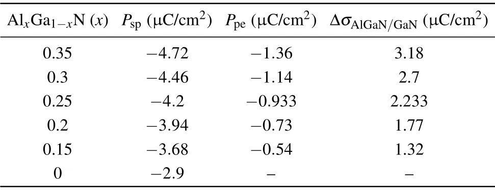
Table 1. Calculated polarization values in the AlxGa1-xN/GaN heterostructure.

Fig.2. (a)Schematic diagram of the device structure of the AlxGa1-xN/GaN MFSHEMT with an FE gate stack of Hf0.5Zr0.5O2/Al2O3 and a non-FE gate stack of HfO2/Al2O3. (b)Polarization effects of the FE/AlGaN/GaN structure with induced surface charge,including AlGaN spontaneous polarization(Psp,AlGaN),AlGaN piezoelectric polarization(Ppe,AlGaN,),GaN spontaneous polarization(Psp,GaN),and FE polarization(PFE).
3. Results and discussion
HfZrO/Al2O3/AlGaN/GaN MFSHEMTs are investigated with varying AlxGa1-xN thickness and Al composition in Figs.3(a)and 3(b). Figure 3(a)presents the curves of the FE polarization in MFSHEMTs with varying Al0.25Ga0.75N barrier layer thickness. The FE polarization of the HfZrO/Al2O3FE film induces a positive FE polarization chargeσFEthat is oriented parallel to the AlGaN barrier layer polarization because of the pinning effect induced from the AlGaN polarization at the FE/AlGaN interface,[41]greatly weakening the controllability of the gate FE effect. With the thinning of the AlGaN barrier layer, the slope of FE polarization curves increases, subsequently enhancing the switching efficiency of the FE polarization. The polarization value of FE HfZrO/Al2O3dielectrics layer increases with the increase of applied electric field. The polarization of AlGaN barrier layer hinders the increase of FE polarization atVg<0.6 V because of the pinning effect. When conduction band of Al-GaN barrier layer is bent below the Fermi level atVg>0.6 V,electron concentration increases in the oxide/AlGaN interface.The electric field applied on FE HfZrO/Al2O3dielectrics layer suddenly increases, leading to a sudden rise in FE polarization. The results indicate that electron concentration increase in the FE/AlGaN interface atVg>0.6 V,which increases the FE polarization.[37]The barrier height in the AlxGa1-xN/GaN heterostructure increases with the increasing Al composition in the AlxGa1-xN barrier layer, and a higher gate voltage is required to cause an abrupt increase of the FE polarization in Fig.3(b).
In Fig. 4(a), we show the FE polarization of the HfZrO/Al2O3/AlxGa1-xN/GaN capacitors with varying Al-GaN barrier thickness and Al composition. With the thinning of the AlGaN barrier layer, the FE polarization of HfZrO/Al2O3gate stack improves, especially at the high Al compositions. The negative polarization charge of Al-GaN surface in different AlGaN barrier thicknesses are the same between FE HfZrO/Al2O3/AlGaN/GaN and non-FE HfO2/Al2O3/AlGaN/GaN capacitors. Compared with non-FE HfO2/Al2O3/AlGaN/GaN capacitor, FE polarization charge of FE HfZrO/Al2O3/AlGaN/GaN capacitor is increased by the thinning of the AlGaN barrier layer. According to the formula (8), the increase of the FE polarization with the thinning of the AlGaN barrier layer causes the reduction of the negative polarization charge density at the oxide/AlGaN interface in Fig. 4(b). Consequently, the Al-GaN energy barrier reduces and the 2DEG in the channel increases in the FE HfZrO/Al2O3/AlGaN/GaN capacitor compared with that in the non-FE HfO2/Al2O3gate stack in Figs. 5(a)-5(c). Furthermore, the 2DEG density of FE HfZrO/Al2O3MFSHEMTs improves by 30.5%, 58.0%,and 134.3% compared to that of the non-FE HfO2/Al2O3gate stack with Al0.25Ga0.75N barrier thicknesses of 20, 10,and 3 nm, respectively, indicating that the reduction of the 2DEG density is suppressed with the FE polarization enhancement. The 2DEG density distributions and conduction band profiles of the HfZrO/Al2O3/AlxGa1-xN/GaN and HfO2/Al2O3/AlxGa1-xN/GaN structures with a 3-nm AlxGa1-xN barrier thickness and Al compositions of 0.35,0.2,and 0.15 are shown in Figs.5(d)-5(e). The 2DEG density of the FE HfZrO/Al2O3MFSHEMTs with the Al compositions of 0.35,0.2,and 0.15 was 1.16×1013,4.9×1012,and 2.81×1012cm-2atVgs=0 V, representing an increase of 174%,108%, and 95% than that of the non-FE HfO2/Al2O3gate stack,respectively.The 2DEG density of the FE HfZrO/Al2O3MFSHEMTs with AlGaN barrier thickness of 3 nm can be improved by increasing the Al compositions.
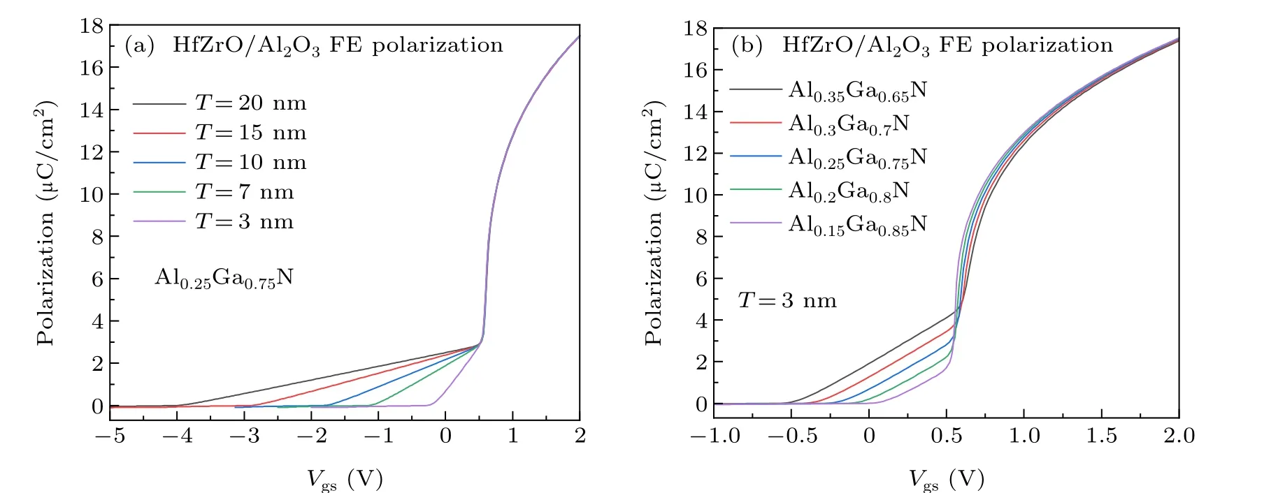
Fig.3. (a)FE polarization of the HfZrO/Al2O3/Al0.25Ga0.75N/GaN capacitors for Al0.25Ga0.75N barrier thicknesses of 20,15,10,7,and 3 nm. (b)FE polarization of the HfZrO/Al2O3/AlxGa1-xN/GaN capacitors for the AlxGa1-xN barrier thickness of 3 nm with Al compositions of 0.35, 0.3,0.25,0.2,and 0.15.
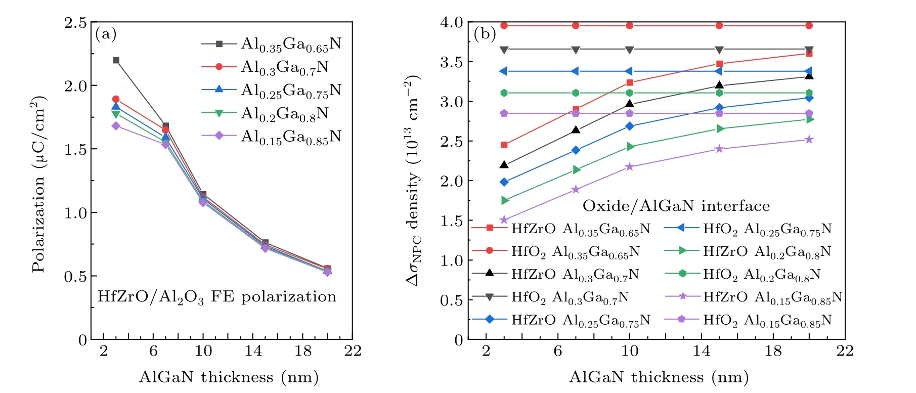
Fig.4. (a)FE polarization of the HfZrO/Al2O3/AlxGa1-xN/GaN capacitors and(b)ΔσNPC density of the oxide/AlGaN interface at Vgs=VTH+1 V for the AlxGa1-xN barrier thicknesses of 20,15,10,and 7 nm. When the AlxGa1-xN barrier thickness is 3 nm,Vgs=VTH+0.5 V.
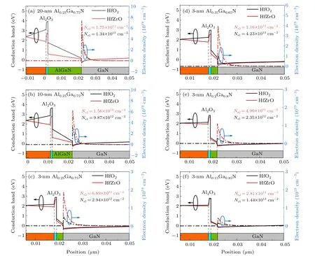
Fig.5. The 2DEG density distribution and conduction band profiles of the HfZrO/Al2O3/Al0.25Ga0.75N/GaN and HfO2/Al2O3/Al0.25Ga0.75N/GaN capacitors for AlGaN barrier thicknesses of 20 (a), 10 (b), and 3 nm (c). The 2DEG density distribution and conduction band profiles of the HfZrO/Al2O3/AlxGa1-xN/GaN and HfO2/Al2O3/AlxGa1-xN/GaN capacitors for 3-nm AlGaN barrier thickness and Al compositions of 0.35 (d),0.2(e),and 0.15(f). The gate voltage is 0 V.
To further evaluate the impact of the AlGaN barrier thickness and Al composition on MFSHEMTs,C-VandIds-Vgscurves are depicted in Figs. 6 and 7. For the AlGaN thicknesses of 20, 15, 10, 7, and 3 nm, the capacitance of FE HfZrO/Al2O3/Al0.25Ga0.75N/GaN structure exhibits an increase of 40.4%, 64.7%, 80.7%, 117.3%, and 285.7%, respectively, over that of the non-FE HfO2/Al2O3gate stack,as shown in Fig. 6(a). This is due to the improving FE polarization of the HfZrO/Al2O3gate stack with the thinning of the AlGaN barrier layer in MFSHEMTs. Similarly,the drive current of FE HfZrO/Al2O3MFSHEMTs with Al-GaN thicknesses of 20, 15, 10, 7, and 3 nm increased by 6.4%, 10.7%, 21.7%, 26.3%, and 71.3%, respectively, compared to that of the non-FE HfO2/Al2O3gate stack,as shown in Fig. 6(b). The bulge in the capacitance curves atVgs=0.6 V is due to the increase of electron concentration in FE/AlGaN interface, which is consistent with the result in Fig. 3. These results suggest that the FE polarization effect of the HfZrO/Al2O3gate stack plays a significant role in improving the electrical properties of MFSHEMTs based on the optimization of the AlGaN barrier thickness. The capacitance of the FE HfZrO/Al2O3/AlxGa1-xN/GaN structure with a 3-nm AlxGa1-xN barrier thickness and Al compositions of 0.35, 0.3, 0.25, 0.2, and 0.15 was 3.14, 3.05, 3.00,2.90, and 2.73 µC/cm2, signifying improvements of 290.0%,282.9%,282.4%,277.2%,and 267.4%than that of the non-FE HfO2/Al2O3gate stack in Fig.7(a),respectively. This can be explained by the increase of the FE polarization with the Al composition when the AlxGa1-xN barrier thickness is 3 nm.Thus, the drive current of the FE HfZrO/Al2O3MFSHEMTs in the 3-nm AlxGa1-xN barrier thinkness with the Al compositions of 0.35, 0.3, 0.25, 0.2, and 0.15, improves by 30.6%,17.6%,11.2%,5.8%,and 5.1%,respectively,over that of non-FE HfO2/Al2O3gate stack in Fig.7(b).)

Fig.6. (a)The C-V and(b)Ids-Vgs curves of the HfZrO/Al2O3/Al0.25Ga0.75N/GaN MFSHEMT and HfO2/Al2O3/Al0.25Ga0.75N/GaN MISHEMT for AlGaN barrier thicknesses of 20,15,10,7,and 3 nm.
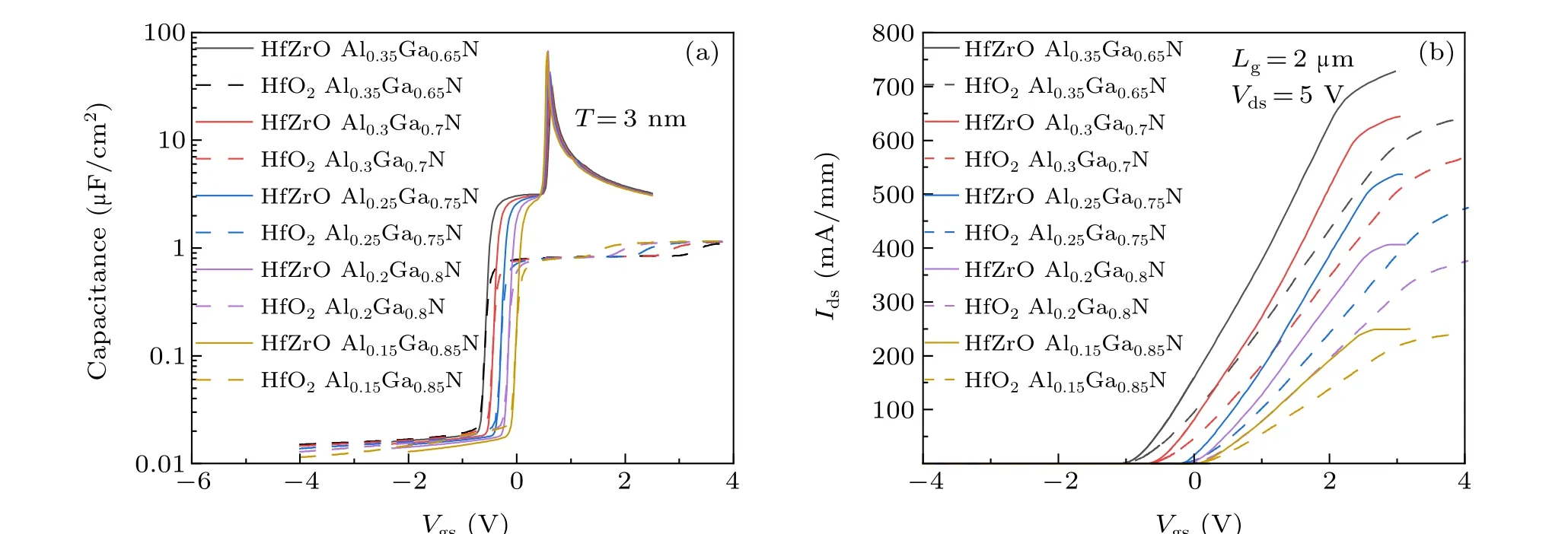
Fig.7. (a)The C-V and(b)Ids-Vgs curves of the HfZrO/Al2O3/AlxGa1-xN/GaN MFSHEMT and HfO2/Al2O3/AlxGa1-xN/GaN MISHEMT for the 3-nm AlxGa1-xN barrier thickness with Al compositions of 0.35,0.3,0.25,0.2,and 0.15.

Fig.8. (a)2DEG density of the FE HfZrO/Al2O3/AlxGa1-xN/GaN capacitor and(b)the difference percentage of the 2DEG density based on FE HfZrO/Al2O3/AlxGa1-xN/GaN and non-FE HfO2/Al2O3/AlxGa1-xN/GaN capacitors with varying AlGaN thickness and Al composition.
Figure 8(a) depicts the 2DEG density of the FE HfZrO/Al2O3/AlxGa1-xN/GaN structure with varying AlGaN barrier thickness and Al composition. When the thickness of the AlGaN layer decreased below 7 nm, the 2DEG density rapidly decreased. However, the reduction of 2DEG density was suppressed when the Al composition was increased. Therefore, to a certain extent, the decrease of the 2DEG density can be suppressed by increasing the Al composition with the thinning of AlGaN layer. To analyze the influence of the FE polarization under different Al compositions and AlxGa1-xN layer thickness on the 2DEG density,the difference percentage of the 2DEG density[(2DEGHfZrO-2DEGHfO2)/2DEGHfO2] was calculated for the FE and non-FE devices in Fig. 8(b). The difference percentage of the 2DEG density with different Al composition was close to 30%,40%,59%,and 82%with the AlGaN thicknesses of 20,15, 10, and 7 nm, respectively. The difference percentage of 2DEG afforded by FE polarization with varying Al composition was basically the same under the same AlGaN thickness from 20 nm to 7 nm, which is consistent with the FE polarization of FE HfZrO/Al2O3gate stack in Fig.8(a). However,the difference percentage of the 2DEG density increased with the Al composition for the 3-nm AlxGa1-xN barrier thickness.The 2DEG density of the 3-nm AlxGa1-xN barrier thickness with varying Al composition exhibits an enormous difference due to the FE polarization of the FE HfZrO/Al2O3gate stack and polarization of the AlxGa1-xN barrier layer, as shown in Figs.4(a)and 5(d)-5(f).The results show that the reduction of 2DEG density can be suppressed by increasing the Al composition for a 3-nm AlxGa1-xN barrier thickness in MFSHEMTs compared to that of the non-FE HfO2/Al2O3gate stack.

Fig. 9. (a) The Gm, (b) SS, and (c) Ion curves of FE HfZrO/Al2O3/AlxGa1-xN/GaN MFSHEMTs with varying AlxGa1-xN thickness and Al composition. The difference percentage curves of(d)Gm, (e)SS,and(f)Ion based on the FE MFSHEMTs and non-FE MISHEMTs with varying AlxGa1-xN thickness and Al composition.
The effect of varying AlxGa1-xN thickness and Al composition onGm,SS, andIonare shown in the Figs. 9(a)-9(c).With the thinning of the AlxGa1-xN layer in MFSHEMTs,Gmincreases in Fig.9(a)andSSdecreases in Fig.9(b)due to the increase of the FE polarization of the FE HfZrO/Al2O3gate stack. Moreover,Iondecreases with the thinning of the Al-GaN layer because of the decrease of the AlGaN polarization in Fig.9(c). As the Al composition increases,GmandIonincrease due to the inducted more 2DEG. A high gate electric field is required to effectively control the large 2DEG induced by the high Al composition in the channel. Consequently,theSSin the device increases with the Al composition. Based on FE HfZrO/Al2O3/AlxGa1-xN/GaN MFSHEMTs and non-FE HfO2/Al2O3/AlxGa1-xN/GaN MISHEMTs,the difference percentage ofGm,SS, andIonare analyzed with varying AlxGa1-xN thickness and Al composition in Figs. 9(d)-9(f).The difference percentage ofGmandIonincrease with decreasing AlGaN thickness, as shown in Figs. 9(d) and 9(f), which is attributed to the enhanced FE polarization in MFSHEMTs.Compared with non-FE MISHEMTs with increasing Al composition,Gmincreases and the decrease ofIonis effectively inhibited for FE device. The difference percentage ofSSfirst increases and then decreases with decreasing AlGaN thickness in Fig. 9(e). As the AlGaN thickness reduces from 20 nm to 10 nm,the degree of 2DEG density decrease is not large,indicating that the FE polarization acting on the abundant 2DEG improves the difference percentage ofSS.Due to the rapid decline of 2DEG with AlGaN thickness from 10 nm to 3 nm,FE polarization acts on a small number of 2DEG,causing the reduction of the difference percentage ofSS.
TheVTHof the FE HfZrO/Al2O3/AlxGa1-xN/GaN MFSHEMTs with varying AlGaN thickness and Al composition is shown in Fig. 10. Clearly,VTHdecreases with decreasing Al composition and AlGaN thickness. When the thickness of the AlGaN layer decreases to a certain extent,the reduction ofVTHhas fewer with the decrease of Al composition because of the lower 2DEG density. Thus,by controlling the AlxGa1-xN thickness and composition in FE MFSHEMTs,VTHcan be adjusted to afford an enhanced device.
Table 2 summarizes electrical characteristics ofGm,SS,Ion, andVTHwith the various AlxGa1-xN thickness and Al composition in FE heterostructure HfZrO/Al2O3/AlGaN/GaN MFSHEMTs. When the thickness of AlGaN barrier decreases to 3 nm, the Al compositions of 0.15 and 0.35 were compared in electrical properties of FE MFSHEMTs. As the Al composition changes from 0.15 to 0.35, theGmandIonincrease from 101 mS/mm to 234 mS/mm and 429 mA/mm to 727 mA/mm, respectively. Meanwhile,VTHincreases only 0.5 V in the Al composition from 0.15 to 0.35, andSSincreases from 63 mV/dec to 68 mV/dec. As a result, the high Al composition with AlGaN thickness of 3 nm has more advantages with the low Al composition in device characteristics.
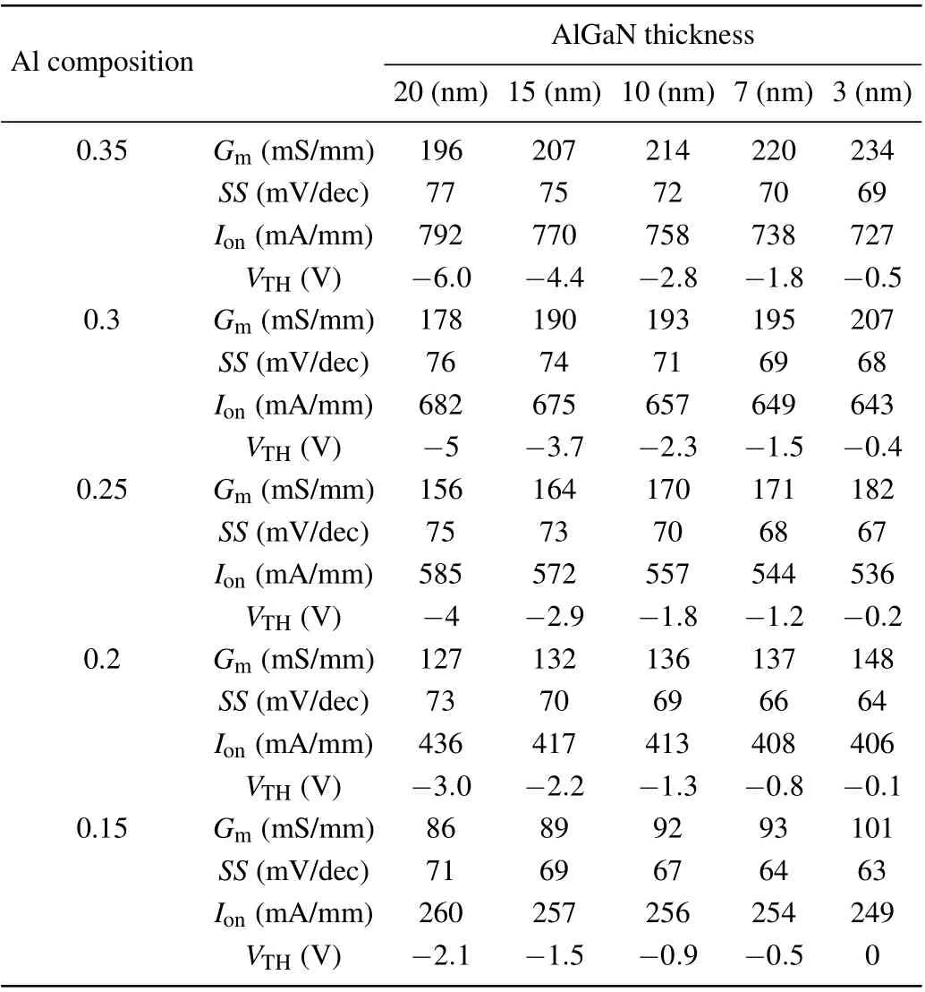
Table 2. The electrical characteristics of Gm, SS, Ion, and VTH with the various AlxGa1-xN thickness and Al composition in FE heterostructure HfZrO/Al2O3/AlGaN/GaN MFSHEMTs.
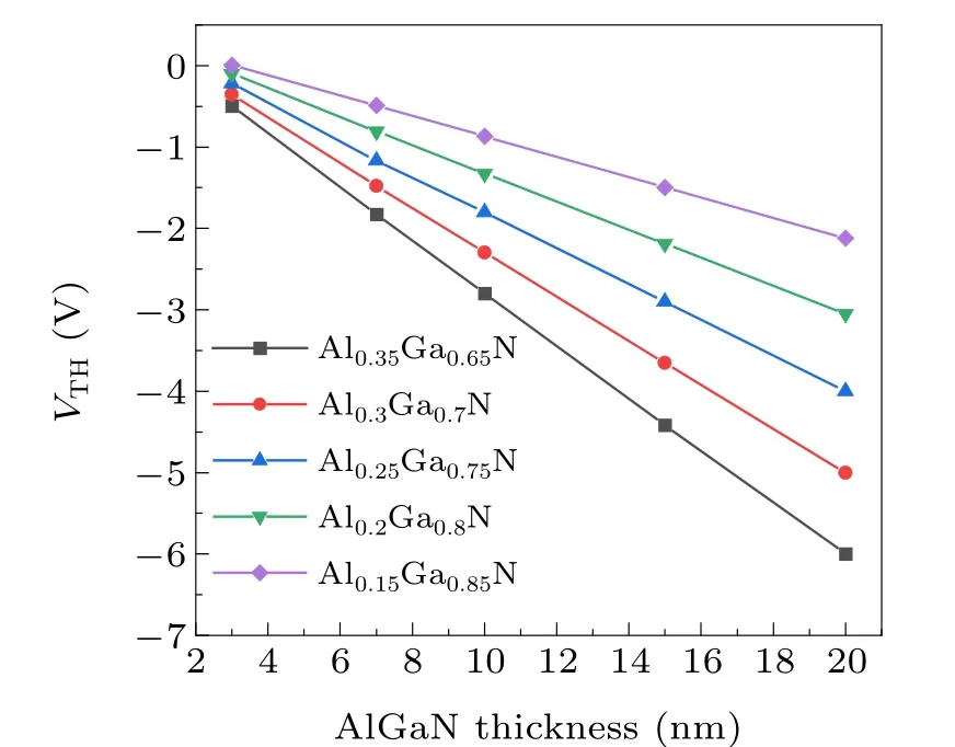
Fig.10. The VTH curves of FE HfZrO/Al2O3/AlxGa1-xN/GaN MFSHEMTs with varying AlGaN thickness and Al composition.
4. Conclusion
In summary, the effect of the AlxGa1-xN thickness and Al composition on the electrical properties was analyzed by simulating FE HfZrO/Al2O3/AlGaN/GaN MFSHEMTs and non-FE HfO2/Al2O3/AlxGa1-xN/GaN MISHEMTs. It is found that the 2DEG density of FE HfZrO/Al2O3MFSHEMTs exhibits an increase of 30.5%, 58.0%, and 134.3%over that of the non-FE HfO2/Al2O3gate stack with Al0.25Ga0.75N barrier thicknesses of 20, 10, and 3 nm, respectively. The decrease of the 2DEG density with the thinning of the AlGaN layer is effectively inhibited in FE capacitors compared to that of the non-FE HfO2/Al2O3gate stack, which is attributed to the increase of the FE polarization in the HfZrO/Al2O3gate stack. Compared to non-FE HfO2/Al2O3/AlxGa1-xN/GaN MISHEMTs, FE HfZrO/Al2O3/AlxGa1-xN/GaN MFSHEMTs afford enhancedGm,SS, andIon. High Al composition with a 3-nm AlGaN barrier layer has a remarkable effect in the improvement ofGmandIon,stemming from the induced large 2DEG and high FE polarization. Furthermore,SSandVTHof FE devices decrease with the reduction of the AlGaN thickness and Al composition, which is beneficial for realizing enhanced devices with high switching performances.
Acknowledgments
Project supported by Guangxi Science and Technology Planning Project (Grant Nos. AD19245066, AA19254015,AD21220150, and AD18281037), the National Nature Science Foundation of China (Grant Nos. 61874036, 62174041,and 62041403), China Postdoctoral Science Foundation(Grant No. 2020M683626XB), the Natural Science Foundation of Guangxi Zhuang Autonomous Region (Grant No. 2018GXNSFAA138025), Guangxi Innovation Research Team Project(Grant No.2018GXNSFGA281004),GUET Excellent Graduate Thesis (Grant No. YXYJRX01), and the Fund from the State Key Laboratory of ASIC&System(Grant No.KVH1233021).
杂志排行

Chinese Physics B的其它文章
- Characterizing entanglement in non-Hermitian chaotic systems via out-of-time ordered correlators
- Steering quantum nonlocalities of quantum dot system suffering from decoherence
- Probabilistic quantum teleportation of shared quantum secret
- Spin–orbit coupling adjusting topological superfluid of mass-imbalanced Fermi gas
- Improvement of a continuous-variable measurement-device-independent quantum key distribution system via quantum scissors
- An overview of quantum error mitigation formulas