Graded composition and doping p-i-n AlxGa1-xAs/GaAs detector for unbiased voltage operation
2022-09-02ZhiFuZhuJiJunZouZhiJiaSunHeHuangQingLeiXiuZhongMingZhangYongGanChenXianGuoShaoTangWangXiuPingYueGuoLiKong
Zhi-Fu Zhu• Ji-Jun Zou • Zhi-Jia Sun • He Huang • Qing-Lei Xiu •Zhong-Ming Zhang • Yong Gan • Chen-Xian Guo • Shao-Tang Wang •Xiu-Ping Yue • Guo-Li Kong
Abstract p-i-n AlxGa1-xAs/GaAs detectors with graded compositions and graded doping were grown and prepared.From the current-voltage and capacitance-voltage measurement results, the devices had good p-n junction diode characteristics, and the electric field strength under an unbiased voltage was 1.7 × 10⁵ Vcm-1. The full width at half maximum and charge collection efficiency of the detectors obtained from energy spectrum measurements of 5.48-MeV alpha particles were 3.04 and approximately 93%, respectively. In this study, we created the most advanced and promising state-of-the-art unbiased detector reported to date.
Keywords Graded composition · Graded doping ·Detector · p-i-n AlxGa1-xAs/GaAs
1 Introduction
Compared with silicon, gallium arsenide (GaAs) is a direct bandgap semiconductor with a high saturation rate high breakdown electric field and radiation resistance.GaAs has been widely used to fabricate infrared photodetectors, high electron mobility transistors, high-speed digital integrated circuits, and high-frequency electronic and microwave devices. Among the currently known semiconductor materials,GaAs has the largest electron mobility(~8500 cm2/Vs) [1] and provides good electrical characteristics for the preparation of high-mobility, fast-response semiconductor devices. Because of its resistance to radiation levels of 10 to 100 million rads and high temperatures up to 200 °C [2], and mature material epitaxial growth and preparation processes, GaAs has attracted much attention in the preparation of nuclear radiation detectors [3-5]. The earliest research on GaAs detectors was conducted by Eberhardt et al. [6]. They used liquid phase epitaxy to epitaxially grow high-purity,high-quality,undoped GaAs on n-GaAs substrates with a thickness of 65 μm and a carrier concentration of 1013cm-3,obtaining an energy resolution full width at half maximum(FWHM)of 20 keV. Owing to the high purity of GaAs epitaxially grown crystals with a defect density less than 104cm-3and carrier lifetime up to several microseconds,the charge collection efficiency (CCE) of the detector was close to 100%[7].Chemykh et al.prepared a Schottky device with a detection area of 80 mm2using GaAs and obtained an energy resolution of 15.5 keV [8]. The detection of charged particles, X-rays, neutrons, and γ-rays has been realized using GaAs-based detectors such as Schottky, p-n,p-i-n, and photoconductive structures, and good experimental results have been obtained [9-11]. In addition,because GaAs is a compound semiconductor, compared with first-generation semiconductors such as Si and Ge,its displacement energy is large (~18 eV), and it is more resistant to irradiation; therefore, it has application prospects in a strong irradiation environment [12]. Although GaAs as a nuclear radiation detector exhibits good characteristics at room temperature,its bandgap is 1.42 eV.To further expand the use of GaAs in some fields, it is necessary to use AlxGa1-xAs to adjust its bandgap. It is well known that the bandgap of AlxGa1-xAs can be changed by adjusting the amount of the Al component in AlxGa1-xAs[13].
Although GaAs detectors exhibit excellent detection performance, they require an external high-voltage power supply. The use of an external high-voltage power supply not only increases the cost and complexity of a system but also increases the reverse leakage current of the detector and deteriorates the FWHM performance of a device.GaAs is a typical III-V direct bandgap semiconductor, and its structure is similar to that of wurtzite. Two of the most notable features of this semiconductor material are its spontaneous polarization effect and piezoelectric electrodes. It has been reported that the polarization effect of AlGaAs grown by metal-organic chemical vapor phase epitaxy (MOVPE) is more than five times that of GaAs.The two-dimensional electron gas produced by the polarization effect of AlGaAs can be used to fabricate HEMT transistors with high electron mobility. The polarization effect of AlGaAs is significant. Devices made of AlGaAs have a strong built-in polarization electric field.Therefore,the strong built-in polarization electric field of AlGaAs can be used to prepare a zero-biased AlGaAs structure nuclear radiation detector. GaAs-based detectors operating at zero bias have long been the focus of research in the field of nuclear radiation detection.
With the improvement in GaAs materials and processing technology, AlxGa1-xAs devices with graded gaps have been realized by adjusting the Al composition to improve device performance [14]. More importantly, the Alx-Ga1-xAs/GaAs heterostructure of the graded bandgap with varied Al compositions induces a built-in electric field[15].Generally, the built-in electric field induced by bandgap gradation is beneficial for the charge collection of electronhole pairs generated in the depletion region of photodetection or radiation detection devices. The built-in electric field improves the device CCE and reduces the device leakage current owing to the reduced bias [16]. Silenas et al. were the first fabricate X-ray and alpha detectors using a graded-bandgap AlxGa1-xAs/GaAs structures with graded compositions [17-19]. They measured the pulseheight spectrum of a241Am alpha-particle source using their graded-bandgap AlxGa1-xAs/GaAs devices and achieved up to 96%CCE without applying a bias voltage to the device.In addition,graded doping in the GaAs epitaxial growth process causes the GaAs energy band to bend,forming a built-in exponential or linear electric field inside the device.The built-in electric field at the base of GaAs is usually produced by a graded doping structure [20, 21].Both graded composition and graded doping structures can achieve a strong built-in electric field at both ends of a device. If the two methods are combined, the device will have a stronger built-in electric field than that of a single structure. To date, an AlxGa1-xAs/GaAs detector that combines graded composition and graded doping into one structure has not been investigated.
In this work, using low-pressure MOVPE, we grew and fabricated a p-i-n AlxGa1-xAs/GaAs detector with Al compositions from 0 to 0.4, graded doping from 1 × 10¹⁶to 1 × 1018cm-3, and using the built-in electric field generated by a GaAs structure to implement a zero-bias voltage device. A p-i-n device structure has a wide range of applications in nuclear radiation detectors owing to its advantages, including a wide intrinsic region, constant junction capacitance, and high reverse bias voltage [22]. The electrical characteristics of p-i-n AlxGa1-xAs/GaAs detectors were measured using Keithley 4200 SCS semiconductor characterization. The radiation detection properties of the detectors were analyzed using a 5.48-MeV241Am alphaparticle source.The primary purpose of this study was to use the built-in electric field of graded composition and graded doping p-i-n AlxGa1-xAs/GaAs to allow a detector to operate without an externally applied voltage.
2 Materials growth and device preparation
The epitaxially graded composition and graded doping p-i-n AlxGa1-xAs/GaAs layers used in these experiments were grown on 400-μm thick 2-in. (100) n+-GaAs substrates by MOVPE. Its structure is shown in Fig. 1a. A 100-nm thick n-GaAs buffer layer with 1 × 1018cm-3of doping concentration was necessary. The thickness of the grown n-AlxGa1-xAs was 3 μm. The Al composition decreased linearly from 0.4 to 0, and the doping concentration decreased from 1018to 1016. The thickness of the undoped i-GaAs was 1 μm, and its concentration was 1015cm-3.The thickness of the grown p-AlxGa1-xAs was 5 μm, the Al content increased linearly from 0 to 0.4, and the doping concentration increased from 1 × 10¹⁶to 5 × 1018cm-3. The last growth on top of the p-GaAs layer was a very thin p-GaAs cap layer with a thickness of 100 nm and a doping concentration of 5 × 1018cm-3as acontact layer to prevent oxidation of the p-AlxGa1-xAs layer surface and to form an ohmic contact. The total thickness of the p-i-n AlxGa1-xAs/GaAs was 9.2 μm.
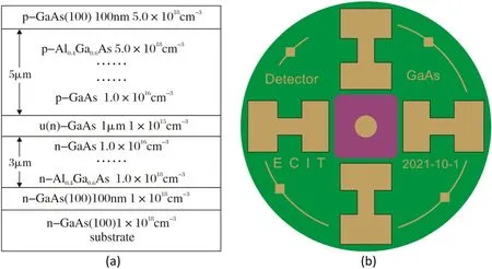
To prepare p-i-n AlxGa1-xAs/GaAs devices,an AuBe alloy with a thickness of 300 nm was deposited on the p-GaAs surface as p-type ohmic metallization,and an AuGeNi alloy was deposited on the back of an n-GaAs substrate with a thickness of 800 nm by e-beam co-evaporation. Finally,heat treatment was carried out at 350 °C for 900 s in N2in a furnace. p-i-n AlxGa1-xAs/GaAs devices with diameters of 1 mm were prepared using planar technology.The back of the device with the AuGeNi alloy layer was mounted on a goldplated printed circuit board(PCB)with silver paste,and the front of the device was wire-bonded to the PCB pad with a 25-μmdiameterwiretopreparethedetectors.Aphotographof the device preparation process is shown in Fig. 1b.The current-voltage(I-V)and capacitance-voltage(C-V)electrical characteristics of the detectors were determined using Keithley’s 4200 SCS parameter analyzer to perform semiconductor characterization at room temperature protected from light.Radiation characteristic measurements were taken using a standard pulse-height analysis Ortec setup.The detector was connected to an Ortec 807 vacuum chamber via an SMA connector.The Ortec setup was composed of a charge-sensitive preamplifier 142A, a shaper amplifier 572A with a shaping time of 1 μs, and a multichannel pulse-height analyzer 927.The spectrum of count versus channel numbers was viewed on a computer using Maestro software.
3 Theoretical simulation and experimental assembly
3.1 Carrier transport and energy band diagram
When the incident particle irradiates the AlxGa1-xAs/GaAs p-i-n detector, electron-hole pairs (carriers) are generated in the AlxGa1-xAs/GaAs p-i-n detector owing to the ionization effect. The transport process of carriers in the detector is complicated and mainly includes thermal,field, and thermal field emissions. A band diagram is the most suitable form of expression to clearly describe the carrier transport process. The energy band diagram of the AlxGa1-xAs/GaAs p-i-n detector is shown in Fig. 2.Compared with the general homogeneous p-i-n junction detector, the AlxGa1-xAs/GaAs p-i-n detector designed in this study was a heterogeneous p-i-n junction that introduced changes in Al composition and doping concentration in both the p- and n-type AlGaAs layers.
Because p-AlGaAs and n-AlGaAs exist on both sides of the intrinsic GaAs, the Al content of the p-AlGaAs increased linearly from left to right, and that of the n-AlGaAs increased linearly from right to left.
As shown in Fig. 1a, the structure of the detector was a heterogeneous p-i-n junction, in which both the p- and ntype AlGaAs layers introduced changes in the Al composition and doping concentration as the thickness increased.Owing to the change in Al composition and doping concentration,the conduction band of the p-type AlGaAs layer bent upward, and the valence band of the n-type AlGaAs layer bent downward. Owing to the presence of p-AlGaAs and n-AlGaAs on both sides of the undoped i-GaAs, a gradually changing p-i-n heterojunction was formed inside the device owing to the graded change in the Al composition, and a strong built-in electric field from the n- to ptype was achieved. The electron-hole pairs generated by ionization were collected by the positive and negative electrodes of the device to generate electrical signals. The carriers in the area were easier to collect and improved the CCE of the device providing the detector with a high sensitivity and ability to perform efficient detection. In addition, because the p-AlGaAs and n-AlGaAs concentrations on both sides of the i-GaAs exhibited a trapezoidal change and owing to the influence of the built-in electric field, the actual depletion region of the device was wider than that of the intrinsic region.
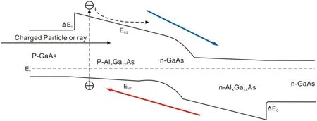
Fig. 2 Band structure of device where Ec is the conduction band minimum, Ev is the valence band peak level, Evac is the vacuum level, and EF is the Fermi level
Lee et al. used the I-V characteristics of a p-n junction to experimentally verify that electron thermionic emission is the main carrier transport mechanism of an AlxGa1-xAs/GaAs heterojunction bipolar transistor [23]. Chen et al.studied the current transport in graded p-n AlxGa1-xAs/GaAs heterojunction diodes by employing a thermal diffusion model[24].Their research results suggested that the injection efficiency of carriers can be significantly improved by inserting a certain thickness of intrinsic layer into a graded AlxGa1-xAs/GaAs heterojunction.
3.2 Simulation
Abrupt or uniformly doped p-n junctions could not be used to analyze the characteristics of our devices. Therefore,we introduced the P-S model to analyze the electrical characteristics of our devices[25].This model obtained the built-in potential, depletion region width,and electric field distribution of the device by solving the Laplace equation,which can also be used to analyze the electrical characteristics of a linear graded junction. According to the P-S equation, the depletion region width WDand built-in potential Vbiof the device are expressed as

where ε0is the vacuum dielectric constant, εsis GaAs(εs=13.1), q is the electron charge, G is the graded constant of the doping concentration, k is Boltzmann’s constant, T is the absolute temperature, and niis the intrinsic carrier concentration.
It can be seen from Eqs. (1) and (2) that after introducing the graded constant G of the doping concentration,the depletion region width WDand the built-in potential Vbiof the device are related. The depletion region width is proportional to the square root of the built-in voltage,which is not the case for conventional p-n junctions. After determining the depletion region width WDand the built-in potential Vbi,the maximum electric field of the device can be obtained as

The built-in potential and depletion region width WDof the device structure shown in Fig. 1 were calculated using MATLAB. As shown in Fig. 3a, the relationship between Vbiand the graded constant G of the doping concentration was linear. The higher the G, the greater the Vbi. When G was 1018cm-3, Vbiwas approximately 1.82 V. However,there was a nonlinear relationship between WDand G.The lower the doping concentration, the larger the width of the depletion region. Because the device structure was a p-i-n type, regardless the doping concentration, the width of the depletion region of the device was always greater than 1 μm. When G was greater than 1015cm-3, the width of the depletion region was greater than 1 μm,but the change was not obvious. As shown in Fig. 3a, increasing the doping concentration increased the built-in voltage,and the corresponding width of the depletion region was narrowed because the effective carrier concentration changed when the doping concentration increased.
Under the action of an electric field, the carriers in the depletion region moved toward both ends of the electrode.The electric field strength determines the mobility and saturation velocity of carriers in a device. Equation (3)shows that the electric field strength is proportional to the square root of a device’s total voltage, while the electric field strength of a conventional p-n junction (E = -V/WD)is proportional to the built-in voltage. The relationship between the device’s electric field strength and doping concentration was simulated as shown in Fig. 3b. The electric field strength increased with an increase in the graded constant G of the doping concentration. When G was 1015cm-3, the electric field strength of the device reached 1.7 × 10⁵V/cm. This value was obtained without external bias voltage. Compared with conventional uniformly doped p-n junction diodes, the electric field strength of our device was relatively close to the maximum theoretical electric field of GaAs (~5 × 10⁵V/cm).

Fig.3 (Color online)Theoretical simulation of detector:a relationship between depletion region width and built-in voltage and graded constant and b relationship between device electric field strength and doping concentration
The range of 5.48-MeV alpha particles in GaAs was simulated using SRIM. As shown in Fig. 4, the alpha particle of 5.48 MeV had a range of approximately 18.4 μm in GaAs. According to our device structure, the depletion region width was approximately 1 μm. According to our device structure, 325 KeV was absorbed by GaAs for a depletion region of 1.19 μm(from theoretical simulations).
3.3 Experimental assembly

Fig. 4 Range of charged particles in GaAs from SRIM program
For semiconductor detectors, the ionization energy of the incident rays in semiconductor materials is much smaller than that of gas detectors (~30 eV). Therefore,semiconductor detectors have a higher energy resolution.The electron-hole pairs generated by incident radiation in the intrinsic region of a detector are collected by the electrodes under the action of an electric field. During measurements, because the energy gap of GaAs is 1.4 eV,external light and various electromagnetic radiations in nature interfere with the detector. To shield the detector from external electromagnetic and light interference, an Ortec 807 vacuum chamber was used. The alpha particles were partially lost in the air before reaching the detector.A mechanical pump was used to evacuate the vacuum chamber to reduce the energy loss of the incident rays in the air. The vacuum pressure in the chamber was less than 1 Pa. The electron-hole pairs generated in the intrinsic region cannot be directly collected by subsequent circuits,and a preamplifier must be added at the back end of the detector. There are three types of preamplifier: current,voltage, and charge. To obtain higher-energy-resolution characteristics, a charge-sensitive preamplifier with lower noise is more suitable for energy spectrum measurements.This system used an Ortec 142A as the detector rear signal amplifier. Usually, the rise time of an output signal from a 142A amplifier is only a few nanoseconds,and the fall time is very long, approximately several microseconds or even tens of microseconds.Neither the voltage amplitude,pulse rise time, nor output signal from a charge amplifier is sufficient for data acquisition. It is also necessary to shape the pulse and amplify the output signal from a chargesensitive preamplifier. In this experiment, an Ortec 572A shaping amplifier with adjustable forming time and magnification was used. Data were acquired using an Ortec 927-pulse multichannel analyzer with a 16 k ADC. The experimental setup is shown in Fig. 5. The241Am alpha source (5.48 MeV)used in the measurement was a surface source with a diameter of 30 mm, an effective emission area of 25 mm, and a thickness of 2 mm.
Before the measurement, a mechanical pump was used to evacuate the alpha source and detector to less than 1 Pa.A collimator was not used between the241Am alpha source and detector.The distance between the241Am alpha source and detector was 3 mm.
4 Results and discussion
4.1 I-V measurement
The current expression for an ideal p-n junction diode is[26]

where ISis the reverse saturation current, V is the detector applied bias voltage, Dnand Dpare the minority electron and minority hole diffusion coefficients, respectively, np0and pn0are the minority electron and minority hole densities in thermal equilibrium, respectively, and Lnand Lpare the diffusion lengths of minority electrons and minority holes, respectively.
The p-i-n structure is a special case of the p-n structure;therefore,the device current of a p-i-n structure can also be calculated using Eq.(3).Compared with a conventional pn junction, the reverse leakage current of a p-i-n type device structure is smaller.For nuclear radiation detectors,the bias voltage applied to both ends of a detector is negative;that is,the detector operates in the reverse bias mode.The reverse leakage current of a device was mainly formed by the diffusion movement of minority carriers.
Current vs. forward and reverse voltage measurements for the p-i-n AlxGa1-xAs/GaAs detector were taken at room temperature using a Keithley Model 4200-SCS semiconductor characterization system. As shown in Fig. 6a, the forward I-V characteristic of the detector exhibited a threshold voltage of 0.95 V(forward current:1 mA), which indicates good p-n junction I-V characteristics. When the forward and reverse biases were 1 V, the currents were 0.185 mA and 0.3 nA, respectively. The current ratio of the forward and reverse biases was 1.62 ×10⁶at 1 V, indicating the high quality of the diodes. The high built-in voltage and high current ratio observed for the p-i-n AlxGa1-xAs/GaAs detector structure indicated that tunneling through the narrow triangular barriers was an effective transport mechanism for carriers in the space charge region of the graded composition and grade-doped p-i-n layer.
4.2 C-V measurement
Based on the relationship between the reverse bias voltage and space charge region width, the C-V method can be used to calculate the width of the depletion region of the device.The expression for the junction capacitance and voltage of the device is
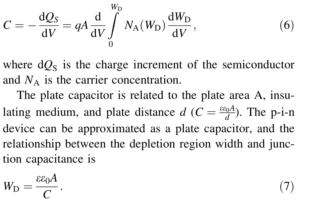
According to Eqs.(6)and(7),the depletion region width of the detector can be calculated by measuring the C-V characteristics of the device.
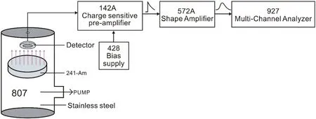
Fig. 5 Schematic diagram of energy spectrum measurement used in experiment

Fig.6 Electrical characteristics of detector:a I-V characteristics of detector with 1-mm detection diameter under forward and reverse biases and b C-V characteristics and depletion width vs reverse bias voltage relationship
The depletion width of the detector can also be determined from the experimentally measured capacitance.The C-V characteristics of the p-i-n AlxGa1-xAs/GaAs were measured using a Keithley 4200, and the relationship between the device depletion width and reverse bias voltage was derived. As shown in Fig. 6b, as the reverse bias voltage increased, the depletion region width increased.The width under reverse bias voltage increased from 1.08 μm at 0 V to 1.6 μm at 30 V. The depletion region width under zero bias was slightly larger than 1 μm, indicating that the results from the theoretical calculations and experimental measurements were consistent. The width measured experimentally included the thickness of the i-GaAs layer 1 and the p- or n-GaAs (1016cm-3) layer doped with thinner graded components owing to the builtin potential of the structure as shown in Fig. 1. Thus, the depletion region width was greater than that of i-GaAs under zero bias in the structure of Fig. 1.
4.3 Alpha particle response
The241Am isotope source emitted charged particles with energies of 5.48 MeV and γ-rays with an energy of 59.6 keV. To demonstrate the insensitivity of our detector to gamma rays, a 1-mm thick aluminum foil was placed between the detector and radioactive source. No pulsed electrical signal was observed at the output of the chargesensitive preamplifier using an oscilloscope. This may be because the interaction of the 59.6-keV X-ray with the detector was mainly owing to the photoelectric effect, and the effective thickness of our detector was only 1.05 μm.It is also possible that the signal was drowned in noise.Further optimization schemes are needed for the detection of X-rays, including material quality improvement, lowtemperature measurement, and the use of supporting lownoise nuclear electronics.
The single-particle pulse signal observed using the digital oscilloscope is shown in Fig. 7. This electrical signal originated from charged particles emitted by the241Am isotope source. The electrical signal was connected to the output terminal of the 142A charge-sensitive preamplifier using a BNC coaxial cable. The bias voltage of the detector was 0 V. As shown in Fig. 7, the signal noise was very small at approximately 5 mV, the voltage amplitude of the output signal was approximately 200 mV,and its signal-to-noise ratio was approximately 40. The noise mainly consisted of detector and electronic system noise. According to the 142A datasheet, its equivalent noise was approximately 3.4 keV. However, the detector noise mainly included thermal, flicker, and shot noises.Thermal noise is mainly caused by the movement of carriers at thermal equilibrium, flicker noise is related to the frequency of the signal and originates from the surface effect of the device, and shot noise is caused by the dispersion of current-forming carriers. Among these three types of noise, shot noise is the main noise of a detector and is related to a detector’s saturation current.The smaller the reverse saturation current, the smaller the shot noise;that is,the smaller the detector noise.For p-i-n devices,the junction capacitance is equivalent to the plate capacitance;therefore, the noise of a detector is relatively small.However, noise affects the energy resolution of a detector.

Fig.7 Electrical output signal of 142A charge-sensitive preamplifier observed by digital oscilloscope after 5.48-MeV charged particles irradiated the detector
Before measuring the spectral response of our detector,a commercial ORTEC Si-passivated implanted planar (Si-PIPS) charged-particle detector was used to calibrate a standard 5.48-MeV241Am alpha source (certificate number: 14AM4A1007), and the CCE of the detector was assumed to be 100%. Owing to ionization energy, bias voltage,and crystal quality,it is impossible to use uniform parameters to combine the Si-PIPS and AlxGa1-xAs/GaAs detector pulse heights in the energy spectrum measurement of AlGaAs detection. Without changing the Ortec main amplifier, the energy-height spectra of the AlxGa1-xAs/GaAs and Si-PIPS detectors using a241Am source were measured. In the energy spectrum measurements shown in Fig. 8, the FWHM from the electronic system was not considered. The energy spectrum response of the p-i-n AlxGa1-xAs/GaAs detector with a 1-mm sensitive diameter to a standard241Am alpha source was measured using Ortec’s nuclear electronics system under various reverse biases from 0 to 20 V at room temperature obtained by single-peak Gaussian fitting as shown in Fig. 9a.To further analyze the performance of the p-i-n AlxGa1-xAs/GaAs detector,the relationship between the reverse bias voltage,peak position, and FWHM is shown in Fig. 9b.
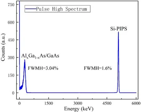
Fig. 8 Energy spectra of Si-PIPS at - 85 V and AlxGa1-xAs/GaAs at 0 V measured using a 241Am source
As shown in Fig. 9b, as the reverse bias voltage increased,the peak position shifted to the right of the highenergy region from 340 keV at 0 V to 342 keV at 20 V.The higher the applied bias voltage,the wider the depletion region. The energy of the particles deposited in the depletion region increased. The peak position only increased by 2 keV, but the reverse bias increased from 0 to 20 V. However, when the bias voltage was 15 V, the peak position no longer shifted to the right,and the change in the peak position was only 0.5%. The device was completely depleted when the bias voltage was 15 V. In addition, according to our calculations, the FWHM increased as the reverse bias increased. The FWHM increased from 3.04% at 0 V to 3.65% at 10 V. When the reverse bias voltage increased to 20 V, the FWHM increased by 3.76%. The increases in FWHMs at reverse biases of 10 V and 15 V were the same at 3.65% because the increase in the reverse bias voltage across the device increased the thermal noise of the device and caused a larger FWHM instead of a wider depletion layer.
Combining the peak position and FWHM, although the device was completely depleted at a 15-V bias voltage,the electron-hole pairs generated by the alpha particles in the depletion region were partially recombined and changed the FWHM owing to the presence of impurities or defects in the epitaxially grown p-i-n AlxGa1-xAs/GaAs. We used SRIM to simulate the depletion region width of 5.48-MeV alpha particles in our detector, and the depletion region width with a peak position of 340 keV at zero bias was approximately 1 μm. Therefore, as shown by the energy spectrum response in Fig. 9b, although the bias voltage increased, the peak shift to the right was not obvious and only changed from 340 to 342 keV. However, the FWHM decreased from 3.04 to 3.76%. We believe that the graded composition and doped p-i-n AlxGa1-xAs/GaAs detector had a sufficiently strong built-in electric field to nearly deplete the 1-μm i-GaAs.Under zero bias,the C-V results were almost consistent with the width of the depletion region obtained from the spectral response. The thickness of the intrinsic region of our detector was thinner,and 5.48-MeV alpha particles deposited less energy into the intrinsic region.The energy deposited in the 1.19-μm thick intrinsic region was approximately 325 keV from the SRIM simulation. Hence, the energy detected by the detector was far less than the 5.48 MeV energy emitted from the241Am.
The calculation of CCE is obtained as [27]

where CH is the channel number corresponding to the peak position, a is the voltage correction factor, E is the energy of the incident particle, ε is the average energy required to create an electron-hole pair,m is the DAC conversion gain of 972,GPis the gain of the 142A,and GAis the gain of the 572A.
According to Figs. 8 and 9b, the CCEs of the detectors were estimated as shown in the inset of Fig. 9b. The CCE of the detector changed from 92.7%at 0 V to 93%at 20 V.When the bias voltage increased, the CCE did not change significantly, indicating that the detector CCE was nearly saturated. Regardless the increase in the detector bias voltage,the detector CCE could not reach 100%.This was mainly owing to the existence of various defects in the epitaxially grown GaAs, such that the electron-hole pairs generated by the incident particles were partially recombined by the defects and not collected by the electric field at both ends of the electrode. However, if the CCE is calculated based on the energy emitted by the radioactive source and energy received by the detector, the CCE is approximately 6.2%.
5 Conclusion
A p-i-n AlxGa1-xAs/GaAs structure with graded composition and graded doping was epitaxially grown on a 400-μm thick n-GaAs substrate using MOVPE. Composition and doping concentration changes are growth methods that change linearly with increasing thickness. p-i-n Alx-Ga1-xAs/GaAs detectors were prepared by depositing a AuBe alloy on p-GaAs and a AuGeNi alloy on n-GaAs,and these detectors were then bound to a PCB using an ultrasonic gold-wire ball bonder. According to the experimental results of the I-V electrical characteristics, it was estimated that the threshold voltage of the detector was 0.95 V.When the applied voltage was 1 V,the ratio of the forward and reverse currents was 1.62 × 10⁶, indicating that the device had good p-n junction diode characteristics.From the C-V measurement results, the depletion region width was approximately 1.08 μ and was consistent with the theoretical simulation results. The theoretically calculated electric field strength of the detector under zero bias was 5 × 10⁵Vcm-1. A standard241Am α source(5.48 MeV) was used to measure the energy spectrum response of the detector when the reverse bias voltage increased from 0 to 20 V.The measurement results showed that when the device reverse bias voltage increased to 20 V, the peak position of the241Am α source did not fundamentally move to the right side of the high-energy region; however, the FWHM of the detector deteriorated.The FWHM of the detector was 3.04% at zero bias and 3.76% at 20 V. The graded composition and grade-doped p-i-n AlxGa1-xAs/GaAs detectors had a strong built-in electric field from the n- to p-type in the junction region owing to the graded change in Al composition and change in doping concentration. Therefore, the detector was practically depleted under zero bias. Owing to defects in the epitaxially grown GaAs crystal,the CCE of the detector did not reach 100% when the external bias voltage was increased. The CCE under zero bias was not significantly improved compared to that under 20 V.This shows that the built-in electric field of the detector was large enough for the CCE of the detector to reach the maximum value.p-i-n AlxGa1-xAs/GaAs detectors that operate without an externally applied voltage will have broad application prospects in neutron logging, environmental monitoring,oil and gas exploration, underground prospecting, and nuclear power station radioactivity detection.
Author contributionsAll authors contributed to the study conception and design. Material preparation, data collection and analysis were performed by Zhi-Fu Zhu, Ji-Jun Zou, Zhi-Jia Sun, Huang He,Xiu-Ping Yue and Shao-Tang Wang.The first draft of the manuscript was written by Qing-Lei Xiu, Zhong-Ming Zhang, Yong Gan, Chen-Xian Guo and Guo-Li Kong all authors commented on previous versions of the manuscript. All authors read and approved the final manuscript.
杂志排行
Nuclear Science and Techniques的其它文章
- Determining absolute value of thermal neutron flux density based on monocrystalline silicon in nuclear reactors
- Transition edge sensor-based detector: from X-ray to γ-ray
- Commissioning of laser electron gamma beamline SLEGS at SSRF
- Imaging internal density structure of the Laoheishan volcanic cone with cosmic ray muon radiography
- Silicon PIN photodiode applied to acquire high-frequency sampling XAFS spectra
- Improvement of machine learning-based vertex reconstruction for large liquid scintillator detectors with multiple types of PMTs