Transition edge sensor-based detector: from X-ray to γ-ray
2022-09-02ShuoZhangJingKaiXiaTaoSunWenTaoWuBingJunWuYongLiangWangRobinCantorKeHanXiaoPengZhouHaoRanLiuFuYouFanSiMingGuoJunChengLiangDeHongLiYanRuSongXuDongJuQiangFuZhiLiu
Shuo Zhang• Jing-Kai Xia• Tao Sun • Wen-Tao Wu • Bing-Jun Wu•Yong-Liang Wang • Robin Cantor • Ke Han • Xiao-Peng Zhou •Hao-Ran Liu • Fu-You Fan • Si-Ming Guo • Jun-Cheng Liang •De-Hong Li• Yan-Ru Song • Xu-Dong Ju • Qiang Fu • Zhi Liu
Abstract A transition edge sensor (TES) is extremely sensitive to changes in temperature, and combined with a high-Z metal of a certain thickness, it can realize highenergy resolution measurements of particles such as X-rays. X-rays with energies below 10 keV have a weak penetrating ability, hence, only gold or bismuth of a few micrometers in thickness can guarantee a quantum efficiency higher than 70%. Therefore, the entire structure of the TES X-ray detector in this energy range can be realized using a microfabrication process.However,for X-rays or γrays from 10 keV to 200 keV, submillimeter absorber layers are required, which cannot be realized using the microfabrication process.This paper first briefly introduces a set of TES X-ray detectors and their auxiliary systems,and then focuses on the introduction of the TES γ-ray detector with an absorber based on a submillimeter lead-tin alloy sphere. The detector achieved a quantum efficiency above 70% near 100 keV and an energy resolution of approximately 161.5 eV at 59.5 keV.
Keywords Synchrotron radiation instrumentation · X-ray spectrometers · Cryogenic detectors · Transition edge sensor
1 Introduction
A transition edge sensor(TES)is an extremely sensitive temperature sensor whose main structure is a superconducting thin film. Under a certain temperature and bias current, it can operate in the transition state between superconducting and non-superconducting [1, 2]. Because the transition region is narrow, the resistance of a TES is extremely sensitive to changes in temperature. The temperature coefficient of the resistance (αI) of a TES is significantly higher than that of traditional semiconductor thermometers; therefore, it has been used in numerous cutting-edge scientific studies [3-11]. For the sake of brevity, this paper mainly introduces work in the fields of X-rays and γ rays.
In the X-ray energy range, the application fields of a TES mainly include synchrotron-based beamline end stations[6-8,12-15],accelerators,electron beam ion traps(EBITs) [11, 16-18], X-ray astronomy [19-21], and electron microscopy [22]. The X-ray flux of beamline stations based on synchrotron radiation and free electron lasers is significantly higher than that of laboratory-level sources.In addition to the rapid analysis of general materials, there is an urgent demand for the energy spectrum measurement of dim and non-point X-ray sources. As a result, the demand for TES X-ray detectors is increasing[6-8,11].TES X-ray detectors have been used in research areas such as low-Z element X-ray emission spectroscopy (XES) [7], X-ray absorption near-edge spectroscopy [23-25], time-resolved X-ray absorption and emission spectroscopy [13-15], and resonant soft X-ray scattering(RSXS)[26].In accelerators,TES X-ray detectors have been used to measure meson atomic energy spectra, such as those of π and κ [11]. TES X-ray detectors have been and will be used for highcharge-state atomic spectroscopy measurements on highcharge-state ion traps [18, 27-29]. In X-ray astronomy,TES X-ray detectors are used in micro-X sounding rocket experiments and will be used in space science observation platforms, such as the ATHENA and HUBS satellites[19-21]. In applications related to electron microscopy,TES X-ray detectors have been introduced into scanning electron microscopy for elemental distribution and valence analysis with high spatial resolutions [22, 30, 31].
In the γ-ray energy range,the application fields of a TES include nuclear clocks [32], nuclear security inspection[33, 34], and nuclear medicine. Nuclear clocks use the change in the nuclear energy level to determine the period.Compared to the traditional atomic clock, the energy level of the nucleus is less affected by the environment. Currently,the main nuclide selected is229Th.To determine the energy level,several institutions in Japan have used TES γray detectors to accurately measure the relevant energy levels [32]. TES γ-ray detectors can also be used for national security inspections.The most important signal of highly enriched uranium (HEU) is the 185.7 keV γ-ray,which is almost identical to the 186.1 keV γ-ray emitted by226Ra present in other materials.The two spectral lines can be easily identified using a TES γ-ray detector [33]. In addition, NIST used a TES γ-ray detector to accurately measure the spectral lines of a plutonium isotope mixture[35].In nuclear medicine,TES γ-ray detectors can be used to detect γ-rays from radioactive materials [36, 37].
After years of development, ShanghaiTech University and its cooperative institutions constructed a TES X-ray detector [38]. Using this detector, elemental analysis was performed on the energy spectra of various materials.This paper presents the energy spectra of coins, stones, and high-purity niobium.The TES detector used for soft X-rays had an absorber with a thickness of several micrometers and a relatively inadequate ability to trap photons above 10 keV. To expand the energy range, the research team combined submillimeter-sized lead-tin alloy balls with the TES to perform energy spectrum measurements for γ-rays and obtained an energy resolution of 161.5 eV at 59.5 keV.
2 Theoretical and instrument descriptions
A TES X/γ-ray detector is a type of microcalorimeter.In this section, the principle and types of microcalorimeters are first introduced, followed by a brief introduction of the structure of the TES X/γ-ray detector and its related systems. Subsequently, several energy spectra are shown, and finally, the structure of the TES γ-ray detector developed on this basis is introduced.
2.1 Principle of microcalorimeters
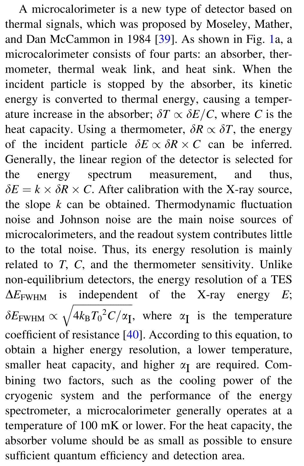
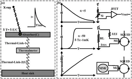
Fig. 1 Principle of microcalorimeters: a shows the main structure and working principle of microcalorimeters.It consists of four parts: an absorber, thermometer, thermal weak link,and heat sink.X-rays are absorbed and converted into thermal signals and then an electrical signal. The thermal signal will finally be conducted to the heat sink before returning to the equilibrium state to wait for the next incident particle.b shows the three thermometers that can be applied to microcalorimeters. Depending on the impedance and signal type of each thermometer, the type of signal amplifier is also different
Depending on the type of thermometer,microcalorimeters are divided into three main types:semiconductor microcalorimeters [41], TES microcalorimeters [1], and metallic magnetic calorimeters(MMC)[42].Semiconductor microcalorimeters use borondoped silicon or transmuted germanium as temperature sensors with low sensitivity to changes in temperature.Owing to its large impedance, a JFET can be used as a signal amplifier. TESs have high temperature sensitivity.However,the transition edge is narrow;hence,it is prone to saturation and has relatively poor linearity. Because of its low impedance, a superconducting quantum interference device(SQUID)is required as a signal amplifier.MMC use paramagnetic materials as temperature sensors, have no saturation problems, and have good linearity. However,owing to its high heat capacity, it requires a lower operating temperature.In addition,it is difficult to multiplex the readout circuit; therefore, MMC are still under development.
Compared with semiconductor thermometers, the improvement in the temperature sensitivity by 10 to 100 times when using a TES makes it more flexible for structural design and material selection. For example, a highspecific-heat material,such as gold(Au),can be selected as the absorber. This change greatly improves the count rate and expands the range of material selection, allowing the use of microfabrication to obtain large arrays. The reduction in the heat capacity limitation of the absorber also makes it possible to bury the source in the absorber;therefore, several research institutes have used this feature to conduct neutrino mass measurement studies [43].
Selection of the absorber material was one of the main points of interest in this study. The time constant of a microcalorimeter can be expressed as τ=C/G, where G denotes the thermal conductance. Once the structure and working temperature are determined, the value of G is relatively fixed. According to this formula, a smaller heat capacity corresponds to a smaller time constant, and according to the expression for δEFWHM, the smaller the heat capacity of the absorber, the higher the energy resolution. Therefore, a small heat capacity corresponds to a high time and energy resolution. The heat capacity of the absorber is C =cv×S×H, where cv is the specific heat capacity per unit volume, S is the area, and H is the thickness.For X-rays and γ-rays,the higher the energy,the stronger the transmission ability. After the upper limit of the expected energy Emax is determined, the thickness Hmin corresponding to Emax and the predetermined quantum efficiency (such as 70%) can be calculated, and the maximum photosensitive area Smax can be obtained.To obtain a larger photosensitive area, the absorber should be chosen to achieve the best trade-off between high-Z and low-specific heat capacity. The specific heat capacity at extremely low temperatures is mainly contributed to by electrons and phonons; materials with higher specific heat capacities also have better conductivities. Therefore, from the perspective of maximizing the photosensitive area,it is desirable to use materials with lower electrical conductivities, such as semi-metals (for example, bismuth) or superconducting materials(for example,lead).To improve the conductance, a layer of Au or copper can be added to the absorber to improve the thermal conductivity.
2.2 Structure of a TES X/γ ray detector
TES X/γ ray detectors include a TES chip, input SQUID, and low-temperature block. The TES chip converts X-rays into current signals, and the input SQUID converts the current signals into voltage signals. The functions of the low-temperature block include low-temperature circuit connections, magnetic shielding, electromagnetic shielding, heat sinks, and infrared windows.
The typical structure of a TES sensor chip is shown in Fig. 2, where the silicon substrate is used as the support structure and heat sink, and the thickness of the silicon material is generally between 300 and 500 μm. Suspended silicon nitride is used as a thermally weak link structure,which can be realized by removing all backside silicon via deep silicon etching. The thickness of the silicon nitride is of the order of submicrometers. A molybdenum-copper bilayer superconducting material is used as a thermometer,and the total thickness is of the order of submicrometers.Superconducting materials, such as molybdenum or niobium,are used as wires with a typical thickness of the order of 100 nm. Using high-Z-value materials as the absorber,the thickness in the X-ray range is typically of the order of a few micrometers, whereas for γ-rays, it will reach the submillimeter level.
The normal resistance of the TES chip used for X/γ ray detection is low,generally at the level of 10 mΩ;therefore,the input SQUID chip is used to convert the current signal into a voltage signal. A typical non-multiplexed SQUID structure is shown in Fig. 3. A single-stage SQUID comprises two Josephson junctions with the same structure.When the current in the TES changes, the voltage across the device changes,and the voltage signal is transmitted to the low-temperature signal amplifier through the cable for further amplification and feedback.

Fig.3 Structure diagram of a single-stage SQUID,which consists of a ring-shaped superconducting coil and two Josephson junctions.The magnetic field generated by the current signal of the input coil will generate a voltage signal across the SQUID,while the magnetic field generated by the feedback coil is opposite to the direction of the input coil, making it work in the linear region [44]
The low-temperature block is responsible for electrically connecting the TES chip and input-SQUID and is also responsible for the thermal connection, refrigerator (cold head), and shielding of electromagnetic/magnetic fields. A low-temperature block is limited by the chip structure and its scientific applications, and its structure varies.
2.3 Auxiliary system of the TES X/γ ray detector
The detector requires a cryogenic system, low-temperature signal amplifier, and data acquisition and analysis system (DAQ) to realize energy spectrum measurement.The following is a brief introduction:
Cryogenic system: The refrigeration system provides low temperature, low vibration, low magnetic field, and low electromagnetic interference environments for the TESX-ray detector, mainly including the thermostat, temperature control system, vibration isolation structure, and magnetic/electromagnetic field shielding system. As mentioned above, the thermostat must reach a temperature of 100 mK or lower.To reduce the temperature fluctuation of a low-temperature X-ray detector, it is generally necessary to control the temperature fluctuation of the thermostat to the order of μK.

Low-temperature signal amplifier: Signal amplification systems based on non-multiplex SQUIDs generally use a SQUID array on a 4 K cold plate to further amplify the signal. Its main function is to suppress the noise of the operational amplifier in a room-temperature circuit. Figure 4 illustrates the principle of feedback amplification.The current signal δIinputfirst generates a magnetic field signal in the SQUID loop,and then forms a voltage signal.The voltage signal is further amplified by the 4 K SQUID array and operational amplifier at room temperature. The operational amplifier passes the signal through the resistor Rfto form a negative feedback, and the feedback coil forms a reverse-changing magnetic field in the SQUID loop, finally reaching a state where the feedback currents δIfand δIinputare proportional to each other,δIf=kf×δIinput. The room-temperature terminal voltage signal is proportional to the low-temperature current signal δV300K=δIf×Rf=kf×δIinput×Rf.
DAQ:The data acquisition and analysis system includes an analog-to-digital conversion module (ADC), a waveform reconstruction module, and an energy spectrum analysis module.
2.4 TES X-ray detectors at ShanghaiTech University and the measured spectrum
Several sets of synchrotron radiation facilities and freeelectron laser facilities have been constructed or are under construction around ShanghaiTech University; therefore,many beamline end stations are also being constructed simultaneously.To meet the energy spectrum measurement requirements of several end stations, ShanghaiTech University built a set of TES X-ray detectors for the X-ray band.The detectors use a 4×4 pixel TES sensor chip,and the area of a single pixel is approximately 0.5 mm×0.5 mm. The TES thin film is a molybdenumcopper bilayer film with a transition temperature of approximately 70 mK with molybdenum leads. The absorber layer is 2.4 μm-thick bismuth with a detection efficiency of 70%at 5.9 keV.The input SQUID chip uses a single-stage SQUID, and the refrigeration system has a minimum working temperature of 23 mK. The low-temperature amplifier adopts 16 SQUID arrays connected in series,and the room-temperature feedback amplifier circuit has a bandwidth of 1 MHz.An ADC board based on a PXIe chassis is used in the DAQ. After the signal is transmitted to the computer, the pulse height is fitted using offline software,the heights are calculated and calibrated, and the X-ray energy spectrum is finally obtained. After preliminary tests, the detector had an energy resolution of 5.2 eV at 5.9 keV. The energy spectrum and fitting curve are shown in Fig. 5.
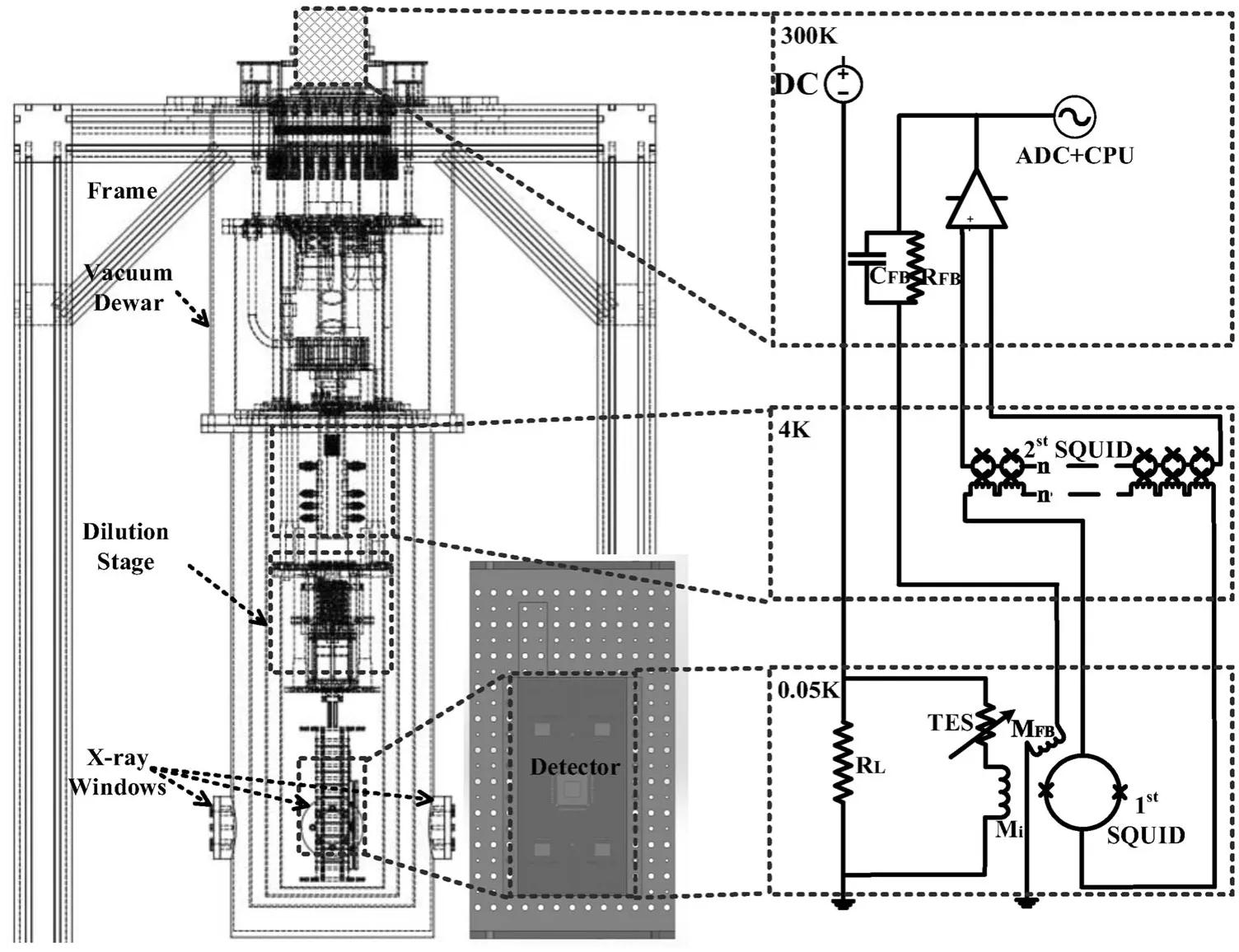
Fig.4 Structure of the auxiliary system: The main structure of the auxiliary system is a set of dilution refrigerators. The low temperature block is installed on a 50 mK cold plate. X-rays are irradiated onto the TES X-ray detector through the X-ray window.The signal is amplified and transmitted from 4 K to 300 K by the low-temperature signal amplifier, which then reaches the DAQ
Two different cases are presented in this paper. In the first case, the composition of the sample was extremely complex,and the relative intensities of the spectral lines of many elements must be determined over a wide energy range. The second case is the measurement of impurity elements in high-purity samples, which required finding faint impurity spectral lines in a strong scattering background environment. In the first case, we used coins and stones as samples. In the second case, we used samples of high-purity (99.95%) niobium.
As shown in Fig. 6, X-rays from the Rh target tube irradiated the coins and stones, and the fluorescence spectrum was collected by the TES X-ray detector.The Rh target voltage was set to 15 kV. Because the K-absorption edge energy level of Rh is approximately 23 keV, the output X-ray is mainly generated by the bremsstrahlung process. The energy spectrum was relatively smooth, and the photon flux changed slowly with energy.
The main content of the coin used for testing was brass,with a nickel-plated pattern in some areas. In the X-ray fluorescence spectrum, we observed clear Kαand Kβspectral lines of copper,zinc,and nickel.At the same time,a lower content of iron and significantly lower content of manganese and silicon were found. Furthermore, clear Lα1and Lβ1spectral lines of Rh were found, which originated from the reflection of the input X-ray by the coin. There were clear Ar Kαand Kβspectral lines in the energy spectrum, which originated from argon in air.

Fig. 5 X-ray energy spectrum of an 55Fe radioactive source. 55Fe emits two X-ray spectral lines with energies of 5900 and 5890 eV,and the detector can clearly distinguish them. After fitting, the detector obtained an energy resolution of approximately 5.2 eV around 5900 eV with Rsquare =0.972

Fig. 6 (Color online) Energy spectrum obtained by irradiating complex composition materials, such as coins and stones, with an Rh target. The Kα and Kβ spectral lines of copper, zinc, nickel, iron,manganese, calcium, titanium, potassium, silicon, argon, and other elements can be clearly observed from the energy spectrum.Owing to the difference in composition, coins and stones exhibit clear differences in the relative intensities of the spectral lines
The stone used for the test was red in color and had a high iron content. In the X-ray fluorescence spectrum, we observed clear Kαand Kβspectral lines of iron,manganese,calcium, titanium, potassium, and silicon. At the same time, a lower iron content and lower levels of cerium,copper, zinc, and gallium were observed. In the spectrum,obvious Rh Lα1and Lβ1spectral lines were seen, which originated from the reflection of the input X-ray by the stone. There were also clear Ar Kαand Kβspectral lines.
The Au target X-ray tube was irradiated with high-purity niobium.The Au target voltage was set to 15 kV. Because the L-absorption edge energy level of Au is lower than 15 keV, the X-ray output of the X-ray tube was mainly composed of a smooth energy spectrum generated by bremsstrahlung and a sharp characteristic peak.

Fig. 7 Energy spectrum obtained by irradiating high-purity niobium with an Au target X-ray tube. From the energy spectrum, Lα1, Lβ1,Lβ3,and Lβ4 of the niobium(Nb)lines can be clearly observed.On the energy spectrum,we can see the obvious Lα1 and Lβ1 spectral lines of gold as well as the Kα line of iron
In the X-ray fluorescence spectrum, the L characteristic line group of niobium was clearly observed. As shown in the enlarged subgraph of Fig. 7, Lα1, Lβ1, Lβ3, Lβ4, and other spectral lines of niobium were observed. There were spectral lines around these that did not correspond to the database.The Kαand Kβlines of Ar were also observed in the X-ray fluorescence spectrum. The Kαlines of lowcontent silicon, potassium, titanium, nickel, and copper shown in the energy spectrum indicate that these were the main components of impurities in the niobium metal.In the energy spectrum, we observed clear Lα1and Lβ1spectral lines of Au and Kαlines of iron,which originated from the reflection of niobium from incoming X-rays. The ratios of the Kαand Kβspectral lines of iron significantly deviated from the theoretical values; the detailed reasons for this must be further explored in future studies. Because the spectral lines of iron did not overlap with other spectral lines, they had no influence on the spectral analysis of the other elements.
In the energy spectrum of niobium, at the low-energy end of the Lα1, Lβ1spectral lines of Au, and Kαof iron,bulge structures were observed. These structures were caused by Compton scattering when X-rays irradiated the sample, which eventually formed a bulge structure at the low-energy end of the elastic scattering peak. Because the Compton scattering bulge is always accompanied by an elastic scattering peak, its existence can be used to determine whether it corresponds to the elastic scattering peak or characteristic spectral line. For example, at the lowenergy end of the spectral line of Lα1of niobium,no bulge structure was observed; therefore, it can be assumed that Lα1of niobium originated from niobium in the sample. At the low-energy end of the iron Kαspectral line,an obvious bulge structure was observed; hence, it can be concluded that most of the iron Kαspectral line did not originate from the sample, but from the iron-containing vacuum parts around the sample.
2.5 Fabrication of γ-ray detector based on the TES
To extend the measurement energy range to 100 keV or even 200 keV, the thickness of the absorber must be increased to the submillimeter level.A lead-tin alloy(63%Pb, 37% Sn)was used as the absorption material. The first reason for choosing this material is that it is superconducting with a small specific heat capacity at low temperatures [3]. Furthermore, lead and tin exhibit a strong absorption effect on X/γ-rays. The thermal transport process of the incident X-rays at different positions of the absorber is not the same, which causes X-rays with the same energy to generate different pulse shapes. To reduce this effect, the absorber was processed into a spherical shape. The spherical structure also reduces the bonding point area,which can reduce the difficulty of bonding.The fabrication process of the entire TES γ-ray sensor is shown in Fig. 8. First, a TES sensor array was prepared, and a small amount of epoxy resin was placed on the TES sensor;subsequently, the pre-processed lead-tin alloy balls were bonded using a robotic arm. After the epoxy resin was cured, the TES X-ray sensor mentioned in the previous chapter was replaced with the TES γ-ray sensor. Finally, a set of TES γ-ray detectors for γ-ray energy range was obtained.
For the size and shape of the absorber,the absorbability of lead-tin alloys with different thicknesses to X-rays and γ-rays with different energies was calculated using the NIST database (PhysRefData). After preliminary calculations, a sphere with a diameter of 0.6 mm could obtain a high detection efficiency in most positions; therefore, the results presented in this paper are based on a lead-tin alloy absorber with a diameter of 0.6 mm. Figure 9 shows the absorption efficiency curves at different distances from the ball axis. It was observed that the position within 0.5 mm from the axis still had a high blocking ability, and the blocking ability sharply declined in the area beyond 0.5 mm.
3 Results and discussion
3.1 Brief description of the experimental setup
We used241Am as the γ-ray source. We coated241Am on a silver-plated metal sheet and then wrapped241Am with aluminum foil.This can effectively reduce the risk of241Am pollution to the surrounding environment while simultaneously reducing the signal intensity of α particles and β particles. The thickness of the aluminum foil was approximately 0.1 mm. This was placed inside the refrigerator 5 mm from the TES γ-ray detector,the surroundings were covered with lead, and then the dilution refrigerator was cooled. After the temperature reached approximately 23 mK, the temperature resistance (R-T) curve of the TES device was measured.The measured transition temperature was approximately 70 mK. Biasing the TES on the transition edge, the energy spectrum of the X-rays and γ-rays generated by the241Am source was measured.
3.2 Time constant and count rate
The response of the TES γ-ray detector to a single γ-ray is shown in Fig. 10. The width of the rising edge was approximately 0.2 ms, and the width of the falling edge was approximately 80 ms. The falling edge of the pulse signal decayed quasi-exponentially. Through fitting, the average time decay constant was τ=8.54±0.06 ms.After 10 τ, the signals returned to the baseline level. According to the estimation of this time constant,the maximum count rate of a single pixel of the detector was approximately 10CPS.This implies that the detector is not suitable for highcount-rate measurement scenarios.

Fig. 8 (Color online)Fabrication process of the TES γ-ray sensor:First,we prepare a TES sensor array, then place a small amount of epoxy resin on the TES sensor. Subsequently,the pre-processed lead-tin alloy balls are bonded by the robotic arm
Fig. 9 (Color online) Absorption efficiency at different distances from the ball axis. The diameter of the ball is 0.6 mm, and the material is a lead-tin alloy
3.3 Linear intervals and saturation energy
241Am decays to Np after the emission of α particles with an energy of approximately 5 MeV and a γ-ray of 59.5 keV with 35.92%probability.When Np is excited,it emits a certain number of fluorescence lines corresponding to the K energy shell and L energy shell. Because there are supporting structures containing elements such as silver,copper, iron, and chromium around the source, the corresponding fluorescence lines can also be observed in the energy spectrum. The energy of each spectral line can be obtained by querying the X-ray fluorescence database http://bruceravel.github.io/demeter/(Demeter) and the manual for241Amhttp://www.nucleide.org/DDEP_WG/introduction.pdf(nucleide.org).According to the settings of the experimental device, it was predicted that the number of pulses corresponding to 59.5 keV photons was the largest.It can be inferred from the right image of Fig.10 that a pulse signal with a height of approximately 1.845 V corresponds to this energy. Through linear estimation, the energy spectrum was found with Kαof copper,Lα1&Lβ1of Np, Kα1&Kα2&Kβof silver, and 26.3 keV &59.5 keV nuclear transition lines of241Am. Using the pulse heights corresponding to these spectral lines to fit the energy values in the database, as shown in Fig. 11, there was a certain deviation in the fitting of one power function(Rsquare =0.9966), and the fitting effect of the quadratic function was excellent (Rsquare =1.000); therefore, the relationship between the pulse height and energy could be expressed by a quadratic function.
It can be seen from the right plot of Fig. 10 that the falling edge of the pulse whose height was lower than 5.5 V decayed exponentially. When the incident particle energy was too high,the pulse appeared saturated with a flat top of approximately 5.5 V. After a certain period of time, it evolved into an equilibrium state at an exponential decay rate.It can be seen from Fig.11 that the pulse height of 5.5 V corresponds to the energy of 220 keV. Therefore, the detector is suitable for γ-ray detection at energies lower than 220 keV.

Fig. 10 Left plot: R-T curve of the TES γ-ray detector. When collecting the energy spectrum,this is biased at the position of 1 mΩ.γ-rays will cause the temperature and resistance of the detector to rise.Right plot: Pulse signals generated by different energy X-rays and γrays have a rising edge width of approximately 0.2 ms and a falling edge width of approximately 80 ms. As shown in the zoomed-in image, the signal corresponding to the nuclear spectral line from 241Am with an energy of 59.5 keV is most dense around 1.845 V

Fig. 11 There is a certain deviation in the fitting of the quadratic function, the fitting effect of the quadratic function is excellent, and Rsquare reaches 1.000
3.4 Energy spectrum and resolution

Fig. 12 Measured energy spectrum of Am241 exhibits spectral lines of Kα of copper,Lα1 and Lβ1 of NP,Kα1 and Kα2 and Kβ of silver,and the 26.3 keV and 59.5 keV nuclear transition lines of 241Am
The detected energy spectrum shown in Fig. 12 was obtained by accumulating the pulse height of each signal calibrated using the least squares fit ‘‘quadratic’’ model inferred by data in Fig. 11. Via Gaussian fitting, the detector had an energy resolution of 161.5 eV at 59.5 keV.However, at lower energies, such as 13.95 keV and 17.75 keV, the detector achieved energy resolutions of 71.6 eV and 69.1 eV. In theory, the energy resolution of TES γ-ray detectors should be independent of the photon energy.Therefore,the achieved results do not seem to be consistent with theoretical expectations. The reason for this phenomenon requires further analysis before conclusions can be drawn. In any case, a possible reasonable explanation for this inconsistency could be as follows: As described in the previous section, the detector was still linear at 59.5 keV; hence, the problem was unlikely to have been introduced by nonlinearity.As mentioned earlier,the higher the energy, the stronger the penetrating ability of the particle;therefore,the thermalization path of the 59.5 keV photon in the absorption body was significantly more complex than that of the 17.7 keV photon,which may be the main reason for this problem.
4 Summary and outlook
In summary, several sets of synchrotron radiation facilities and free-electron laser facilities have been constructed or are under construction around ShanghaiTech University; therefore, several beamline end stations are also being constructed simultaneously.To meet the energy spectrum measurement requirements of these end stations,ShanghaiTech University built a set of TES X-ray detectors for the X-ray band. Using this detector, a composition analysis of complex samples and an impurity analysis of high-purity samples were performed. On this basis, the R&D team prepared a TES γ-ray detector for the energy band below 200 keV. After preliminary analysis and testing,the detector still had a quantum efficiency of 70%near 100 keV and a single pixel count of 10 CPS. It was in the linear working region below 220 keV and had an energy resolution of 161.5 eV at 59.5 keV. However, at lower energies, such as 13.9 keV and 17.7 keV, the detector achieved energy resolutions of 71.6 eV and 69.1 eV. This resolution is two to three times higher than that of existing silicon drift detectors and HPGe detectors, and in the foreseeable future, higher energy resolutions may be achieved with process optimization and more detailed signal analyses.
Although the energy resolution of this detector exceeded those of existing silicon drift detectors and HPGe detectors,its low count rate makes it unsuitable as a replacement for these two detectors for general-purpose measurements.However,the’insensitivity of the detector to doping allows the sample to be buried inside the absorber of the detector.If the absorber is sufficiently thick, the energy of the highenergy particles can be entirely converted into a thermal signal and detected.
For X-ray and γ-ray metrology,this detector can be used for the 4π measurement of radioactive substances with low activity. Long-decay-period radionuclides exist widely in nature, and their existence has a great impact on the development of radiopharmaceuticals and other materials.Owing to its extremely low radioactivity, a 4π measurement with a high energy resolution must be performed to obtain sufficient sensitivity. The TES γ-ray detector can obtain an energy resolution better than that of HPGe on the premise of ensuring 4π measurement and is expected to improve the detection sensitivity by one to two orders of magnitude [45, 46].
The measurement of dark matter is greatly affected by the purity of natural radioactive impurities in liquid, and beta decay energy spectrum data of natural radioactive substances are seriously lacking. This detector can accurately measure the low-energy spectrum of the beta rays from226Ra,40K, and other dark matter-related nuclides.Therefore,this could further depress the sensitivity of dark matter detection.
Neutron decay has been investigated as a possible pathway to explore new physics. Bond beta-decay (BOB)of neutrons is a process in which one neutron decays into hydrogen and an anti-neutrino. Unlike normal neutron decay, this is a two-body process; therefore, it provides an elegant method of studying neutrino helicities [47, 48].However, this process has not yet been observed for low branching ratios, and the number can be as low as 10-6.BOB is a two-body process; the energy carried by the neutrino is fixed, and the remaining hydrogen atoms also have a fixed energy of approximately 325.7 eV.Because of the extremely strong penetrating power of neutrinos, the absorber can only intercept an energy of 325.7 eV; hence,the energy spectrum of this process in the TES X-ray detector appears as a single energy spectral line. Conventional neutron decay is a three-body process, and the sum of the electron and proton energies behaves as a continuum.The energy resolution of the TES X-ray detector is of the order of eV,which can help measure the BOB from the energy spectrum.
Author Contributions Shuo Zhang contributed to the study of conception, system design and construction. Data collection and analysis were performed by Jing-Kai Xia, Bing-Jun Wu. Material design, selection and preparation were performed by Tao Sun,Ke Han, Wen-Tao Wu, Yong-Liang Wang, Xiao-Peng Zhou, Hao-Ran Liu, Fu-You Fan, Si-Ming Guo, Jun-Cheng Liang, De-Hong Li,Yan-Ru Song, Xu-Dong Ju and Qiang Fu. The first draft of the manuscript was written by Shuo Zhang and all authors commented on previous versions of the manuscript. Zhi Liu contributed to the review. All authors read and approved the final manuscript.
杂志排行
Nuclear Science and Techniques的其它文章
- Determining absolute value of thermal neutron flux density based on monocrystalline silicon in nuclear reactors
- Graded composition and doping p-i-n AlxGa1-xAs/GaAs detector for unbiased voltage operation
- Commissioning of laser electron gamma beamline SLEGS at SSRF
- Imaging internal density structure of the Laoheishan volcanic cone with cosmic ray muon radiography
- Silicon PIN photodiode applied to acquire high-frequency sampling XAFS spectra
- Improvement of machine learning-based vertex reconstruction for large liquid scintillator detectors with multiple types of PMTs