Structure,phase evolution and properties of Ta films deposited using hybrid high-power pulsed and DC magnetron co-sputtering
2022-06-29MinHuang黄敏YanSongLiu刘艳松ZhiBingHe何智兵andYongYi易勇
Min Huang(黄敏) Yan-Song Liu(刘艳松) Zhi-Bing He(何智兵) and Yong Yi(易勇)
1Laser Fusion Research Center,China Academy of Engineering Physics,Mianyang 621900,China
2School of Materials Science and Engineering,Southwest University of Science and Technology,Mianyang 621010,China
Keywords: hybrid sputtering,tantalum thin film,structure,hardness
1. Introduction
Tantalum (Ta) films are of interest for technological applications in microelectronics industry due to excellent physical and chemical properties.[1,2]Since non-equilibrium thermodynamic growth is inherent to film deposition, magnetron sputtered Ta films can exhibit the stable BCCα-phase and metastable tetragonalβ-phase, or a mixture of two phases.Theα-Ta film with high hardness (8 GPa–12 GPa), high melting point (Tm≈3000°C), low resistivity (15 μΩ·cm–80 μΩ·cm),and high temperature wear resistance,is the candidate material in many applications such as tool coating,barrel protective coating and Cu/Si diffusion barrier. Theβ-Ta film with higher hardness(18 GPa–20 GPa),higher resistivity(150 μΩ·cm–200 μΩ·cm) but more brittleness can be used as resistors and heaters. Unfortunately,β-Ta phases are prone to phase transition toα-Ta at high temperature,which affects the performance of the Ta film. The coexistence ofαandβphases in films also limited their usability.[3–5]Therefore,deposition pureα-Ta films is critical for the studies of associated films properties. Due to the lower hardness of pureαphase deposited under different preparation methods and deposition conditions, it is necessary to focus on seeking suitable deposition conditions to obtain fine grain and higher hardness ofα-Ta films.
Direct current magnetron sputtering (DCMS) and highpower impulse magnetron sputtering (HiPIMS) are relatively mature magnetron sputtering technologies for preparing Ta thin films. In DCMS, the main feature is to provide good load performance and stable discharge at higher deposition rate. However, only leading toβ-Ta film with inhomogeneous deposition,low density and porous columnar structures,DCMS has a drawback that includes the low degree of ionization (1%–3%).[2]High-power impulse magnetron sputtering(HiPIMS),an IPVD technique combining magnetron sputtering and pulsed plasma discharges,is characterized by high peak power density, plasma density and target ionization (up to 90%)at a low duty cycle(below 10%)and a low frequency(less than 2 kHz),which makes a high degree of ionization and formation of dense, smooth and hard films, even deposition on complex geometries.[2,6,8,9]Unfortunately,in HiPIMS,the deposition rate is only 20%–40% of DCMS and the internal stress and defects in the films can be caused by the unstable arc discharge phenomenon (ARC) under low pressure.[10–12]More recently, the hybrid HiPIMS/DCMS co-sputtering have begun to be used to surmount the defect of the pure HiPIMS technique. For one thing, the mechanism of the “charge exchange” increases the plasma density effectively, as a result,increasing the deposition rate of HiPIMS and improving more efficient and accurate control of the bombardment conditions providing. For another thing,the secondary plasmas produced by DC discharging can effectively prevent the transition from glow to arc in the ignition process of HiPIMS under low pressure. Moreover, the co-sputtering technology is of great significance in improving the quality of the films, refining the grains and improving the compactness.[12,13]Mattiaset al.[14]and Zoitaet al.[15]found that the deposition rate increased as the proportion of DCMS by using DCMS and HiPIMS cosputtering, also the roughness, resistivity and electrochemical oxidation of the Cr films and titanium carbide films were all improved. Guiet al.[12]researching the TiAlCrN ceramic coatings by increasing the Ti target power found that higher Ti target power resulted in stronger ion bombardment, which emerges a denser structure and ultra-smooth surface. To our knowledge,there were most of the co-sputtering to prepare the films like TiN,[16]TiAlN,[12,13,17]and DLC-W[18]by combining DCMS with HiPIMS together. Nevertheless, there were few reports about DCMS/HiPIMS co-sputtering technology for the preparation of Ta thin films in mechanical and electrical properties,especially.
In this paper,Ta films were deposited by DCMS/HiPIMS co-sputtering. The influence of DC powers fraction on the phase structure, morphology, mechanical and electrical properties of Ta films was studied. In the end, this work demonstrated that on the premise of realizing the structure of pureα-Ta,it not only improved the deposition rate of the film,but also surmounted some of drawbacks in HiPIMS to obtain high density and hardness coatings, which is of great significance to the protective coating and diffusion barrier layer.
2. Experiment
All depositions were completed in a JGP560 ultra-high vacuum coating chamber equipped with two pure Ta targets(99.95%purity,76 mm diameter)setting 15 cm away from the magnetron at room temperature in Fig.1. Simultaneously,one single Ta target(A)was driven by a high-power pulsed power supply with the pulsed DC voltage of 650 V, the current of 1000 mA, the power of 150 W, and the repetition frequency of 100 Hz, respectively. Another Ta target(B)was driven by a DC power supply. In this study, for the sake of defending the DCMS power supply from the influence of HiPIMS instability, and ensuring the stability of the deposition process,our experiment was carried out according to the parameters shown in Table 1. Firstly, the deposition rates of DCMS at 100 W and HiPIMS at 150 W power calibrated before experiment was 0.021 nm·s-1and 0.05 nm·s-1, respectively. And then,in Table 1,at those deposition rates,the contribution parameters of DCMS to the Ta film thickness were set as 0%,25%, 50%, 75%, and 100%. Ultimately, the DC powers corresponding to those proportions of 25%,50%,and 75%were calculated as 10 W, 30 W, and 89 W, respectively. The deposition rates of the Ta films under different DC powers were tested by the step meter in Fig. 2(a), and the deposition time calculated for the thickness of 800 nm–1000 nm at the rates were 15000 s,11250 s,7500 s,3750 s,4440 s,respectively.

DC power ratio(%) DC power(W) HiPIMS power(W) Time(s) Deposition rate(nm·s-1)0 0 150 15000 0.0504 25 10 150 11250 0.0762 50 30 150 7500 0.1516 75 89 150 3750 0.2441 100 100 0 4440 0.2093
The deposition rate was increased with the increase of DCMS power under other conditions indicating that the loss of HiPIMS deposition rate could be ameliorated by using additional DC power supply,[19,20]while it decreased at DC-100 W because the only DC target was used without attaching HiPIMS and the sputtering power density was lower than that with HIPIMS. The base pressure and working pressure were 5×10⁻⁶Pa and 0.5 Pa(Ar, 99.999%), respectively. Ta films were deposited to Si wafers(10 mm×10 mm×0.5 mm)with N (111) preferred orientation. All the substrates were ultrasonically cleaned with acetone and alcohol for 10 min, dried with compressed air,and mounted on a substrate holder which was supplied a rotation speed of 10 r/min and a negative DC bias of 60 V for dominating the direction and energy of the deposit to the substrate and improving film uniformity.[2,21,22]
The crystal structures of Ta films were investigated by xray diffraction (XRD) by using Rigaku SmartLab 9 kW with CuKαradiation in grazing incidence (GIXRD, 0.5°). The surface and cross-section of Ta films were detected by a field emission scanning electron microscope (FE-SEM) by using ZEISS sigma 500 (Zeiss, Germany) with BRUKER XFlash 6130. The thicknesses of the films were determined from the cross-sectional SEM observation. Atomic force microscope(AFM)was utilized to establish the three-dimensional topography of the Ta films by using a Bruker Dimension Icon equipment(Billerica,Massachusetts,MA,USA).The hardness and Young’s modulus of the films were measured by nanoindentation tester(U9820A Nano Indenter G200)by using the continuous stiffness measurement(CSM).The resistivities of the Ta films were measured by the Rts-8 four-point probe method.
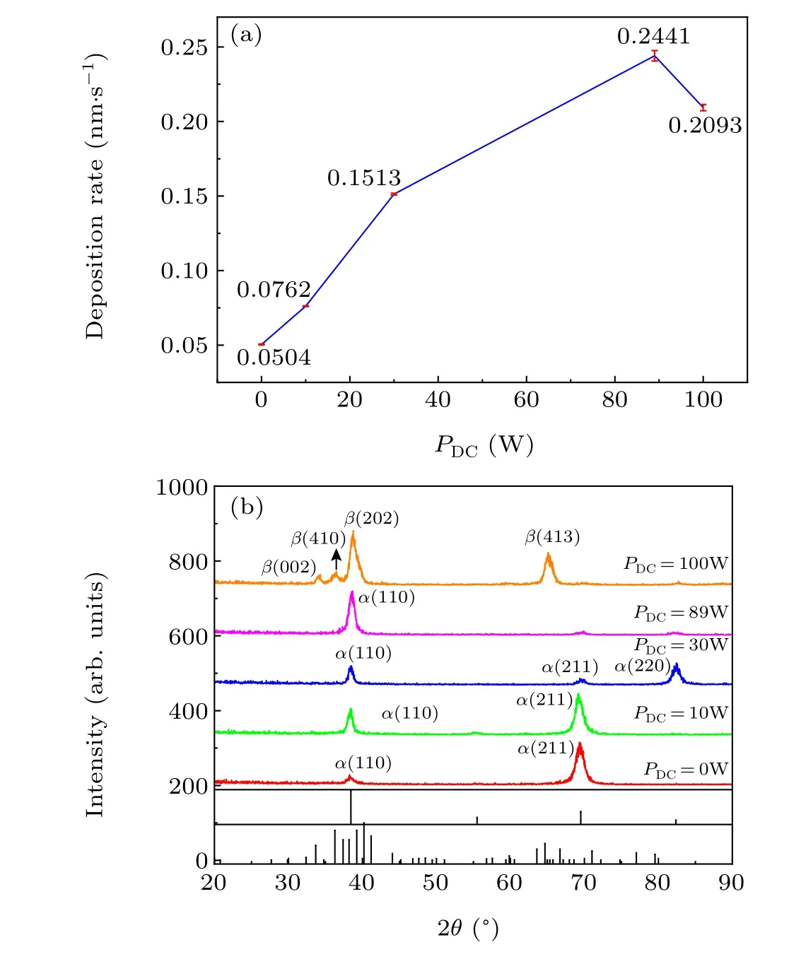
Fig. 2. The deposition rate (a) and XRD diffraction pattern (b) of films at different DC powers.
3. Results and discussion
3.1. Phase evolution of Ta films
Figure 2(b) shows the diffraction patterns (20°–90°) of the Ta films with different DC powers. For DC-100 W, the diffraction pattern showed preferred orientation (202) reflections at 38.78°, and weak (002), (410), and (413) reflections at 34.14°, 36.50°, and 65.15°(JCPDS #00-025-1280), corresponding to pureβ-Ta. In addition, due to tensile stress,the reflections moved to the higher diffraction angles.[23]For the HiPIMS/DCMS co-sputtering at a negative DC bias of 60 V,the(110),(211),and(220)reflections located at 38.47°,69.30°,and 82.53°(JCPDS#00-04-0788),respectively,corresponding to pureα-Ta,which is corresponding to the discussion from Linet al.[19]that tantalum film prepared by HiPIMS wasαstructure when the negative bias voltage was 50 V or greater. For DC-89 W,the film exhibits strong(110)and weak(220)reflections,which shows a phase transformation fromβ-Ta toα-Ta. Theα-Ta(110)peak moved to higher diffraction angles(to smaller lattice spacing)as compared to the diffraction pattern standard indicating that most probably the development of tensile stresses was caused in the Ta films for high deposition rate and sputtering ion energy at higher DC sputtering power such as 89 W.For DC-30 W,the intensity ofα-Ta(110) reflections decreased, while the weak (211) and (220)reflections appeared. No obvious preferred orientation reflections were found. For DC-10 W and DC-0 W,the intensity ofα-Ta (110) reflections decrease further, while stronger (211)reflections were found at 69.51°.
This tend agrees with the previous results that the number of target ions arriving on the substrate/growing film was critical for the formationα-Ta.[14]The results indicated that the phase transformation fromβ-Ta toα-Ta just needs less than 25%Ta ions in co-sputtering. With decreasing DCMS powers in co-sputtering, more Ta ions only led the preferred orientation changes fromα-Ta (110) toα-Ta (211). This suggested that the influence of ionized deposition flux on the observed Ta film phase saturates when the ionic content exceed a certain value.[24]For DC-30 W,α-Ta appeared without preferred orientation during the preferred orientation change,which means the grains sizes were refined and the grains sizes were refined due to the high density of nucleation sites.[24,25]
3.2. Microstructure and morphology of Ta films
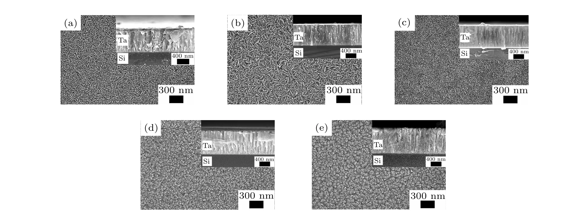
To further investigate the morphology changes, both the surface and cross-section were examined by using FESEM in Fig.3. The thicknesses were about 760 nm,820 nm,840 nm,890 nm,and 990 nm,respectively. For DC-100 W,large irregular spherical particles and a columnar morphology with some crack-like features were found in Fig.3(e),which corresponds to the typical brittle fractures of theβ-Ta.[7,8]For DC-89 W,the surface morphology was similar to Fig.3(e), while it had orderly arranged crystal grain structures with refined grains in Fig.3(d).[2,14,23]Combined with the above XRD analysis,the structure of tantalum film was changed fromβtoα, and the surface morphology was also changed from block to needle by the addition of HiPIMS.The reason for this transition was that the flux and energy of tantalum ions in the plasma were increased by the addition of HiPIMS,and the grown tantalum film would be bombarded by tantalum ions strongly and energetically,which leads toβtowardsαphase and change the morphology.For DC-30 W,extremely fine,dense and uniform crystal grains were obtained in Fig. 3(c), which is consistent with XRD results. For DC-0 W or DCMS-10 W, dense and uniform fine needle-like structures with smaller grains were observed in Figs. 3(a) and 3(b), because of high indexα-Ta(211) preferred orientation reflections,[26]which is shown in Fig.2(b). The change of morphology and microstructure corresponds to the increase in kinetic energy of sputtered metal ions provided by the high sputtering metal ionization rate of HiPIMS as decreased DC powers.Theα-phase film deposited at DC-30 W had extremely fine and dense granular structure,which was the typical characteristic of fine-grained structure.
AFM measurement was utilized to establish the threedimensional topography of the films in Fig. 4. The RMS values (Fig. 4(a)) decreased from 4.14 nm to 1.78 nm as DC power decreased from 100 W to 0 W.The surface ofβ-Ta films deposited by DCMS present large irregular spherical particles,which causes rougher surface.[23]As the DC power decreased,the surface roughness decreased relatively due to the increased ion bombardment. The RMS of the Ta film was 3.22 nm at DC-30 W,relatively higher than that of DC-0 W(1.78 nm).
3.3. Electrical and mechanical properties of Ta films
The electrical resistivity of Ta films was presented in Fig. 5(a). It was found that the resistivity of theβ-Ta film prepared by DC-100 W was the highest. Additionally,the resistivity of theα-Ta film prepared by DC-0 W was the lowest. The resistivity decreased with decreasing DC powers,but only a minor improvement was observed as DC power lower than 30 W.This result was consistent with previous reports that the electrical resistivity was primarily influenced by the phase structures.[27]Besides,the carrier mobility was also inversely proportional to the film’s surface roughness, and the increase in surface roughness also caused an increase in resistivity.
Figure 5(b) plotted the hardness and Young’s modulus of films deposited at different DC powers. For DC-100 W and 0 W, the hardness was 13.60 GPa and 11.41 GPa separately, which is consistent with the hardness characteristics ofβ-Ta andα-Ta films respectively. In particular, the hardness of tantalum film at DC-100 W was significantly lower than that reported in the literature because of its great sputtering atoms ability on the film surface,[19,24,26]which attributes to the grain growth of beta and the large surface roughness.[28–30]However, an abnormal hardness of Ta films with a value of 17.64 GPa was found at DC-30 W. Combining XRD (Fig. 2(b)) and SEM (Fig. 3) results, it can be seen that the Ta film had extremely fine grains at DC-30 W.In the recently published studies,the generous researches which considered on nanoindentation experiments by the molecular dynamics simulation, had shown that the mechanism of metals plastic deformation was closely related to the high nucleation and propagation ability of dislocations.[31–33]The main reasons affecting the hardness and modulus of nanoindentation were the nucleation and proliferation of dislocations in the nanoindentation test probes for pure metal materials.[26,34]According to the Hall-patch relationship,the diffusion and slip of dislocations in the process of plastic deformation could be hindered by the grain boundaries to form a large stress dislocation field so that the ability of resisting plastic deformation was improved.[2,12,23]Notably, the strength and hardness of solid films at DC-30 W were closely related to fine grain strengthening effect. The finer grains and the more grain boundaries behaved so greater, the resistance to the movement of dislocations and other defects that there was the higher of the film hardness.[35–37]

4. Conclusion
In this work, the pureα-Ta films with different microstructures and properties were successfully deposited by DCMS/HiPIMS co-sputtering under different DC powers.The results revealed that the number of Ta ions arriving on the substrate/growing film played an important role in structure and phase evolution of Ta films. By adjusting DCMS powers,hybrid co-sputtering behaved controlling Ta ion to Ta neutral ratios of the deposition flux, which has an important effect on crystalline phase and microstructure of Ta films. Pureα-Ta phase films with extremely fine, dense and uniform crystal grains were obtained, which shows abnormal high hardness(17.64 GPa). Compared with other past researches, three advantages of this DCMS/HiPIMS co-sputtering strategy were found for Ta deposition: (i) phase control and grain refinement, (ii) higher deposition rate, and (iii) suppress the ARC phenomenon of HiPIMS under low working pressure. It will open up for interesting research for specific applications with regard to ion content and deposition rate.
Acknowledgment
Project supported by the National Natural Science Foundation of China(Grant No.51401194).
猜你喜欢
杂志排行

Chinese Physics B的其它文章
- Switchable terahertz polarization converter based on VO2 metamaterial
- Data-driven parity-time-symmetric vector rogue wave solutions of multi-component nonlinear Schr¨odinger equation
- Neutron activation cross section data library
- Multi-phase field simulation of competitive grain growth for directional solidification
- A novel similarity measure for mining missing links in long-path networks
- Effects of electrical stress on the characteristics and defect behaviors in GaN-based near-ultraviolet light emitting diodes