A study on the epitaxial structure and characteristics of high-efficiency blue silicon photodetectors
2022-05-28CHENWeishuaiWANGHaobingTAOJinGaoDanLVJinguangQINYuxinGUOGuangtongLIXianglanWANGQiangZHANGJunLIANGJingqiuWANGWeibiao
CHEN Wei-shuai,WANG Hao-bing,TAO Jin,Gao Dan,LV Jin-guang,QIN Yu-xin,GUO Guang-tong,2,LI Xiang-lan,2,WANG Qiang,ZHANG Jun,LIANG Jing-qiu,WANG Wei-biao
(1.State Key Laboratory of Applied Optics, Changchun Institute of Optics, Fine Mechanics and Physics,Chinese Academy of Sciences, Changchun 130033, China;2.University of Chinese Academy of Sciences, Beijing 100049, China;3.Collage of Science & Engineering, Jinan University, Guangzhou Key Laboratory of Visible Light Communication Engineering Technology, Guangzhou 510632, China)
Abstract:In order to achieve high spectral responsivity of the silicon avalanche photodiode in blue band(400−500 nm),Separated Absorption Control Multiplication (SACM) basic device structure was designed.Based on multiple physical models,the effect of the thickness on the avalanche breakdown voltage and the photocurrent gain of the device and the effect of the doping concentration of the multiplication layer on the optical responsivity were investigated.Comprehensively considering the factors of light responsivity and breakdown voltage,the results show that the device has a low breakdown voltageVbr-apd=34.2 V when the doping concentration of the surface non-depleted layer is 1.0×1018 cm−3,and the thickness is 0.03 μm;the doping concentration of absorption layer is 1.0×1015 cm−3,the thickness is 1.3 μm,the doping concentration of field control layer is 8.0×1016 cm−3,the thickness is 0.2 μm and the doping concentration of double layer is 1.8×1016 cm−3 and the thickness is 0.5 μm.WhenVapd=0.95Vbr-apd,it has higher optical responsivity in blue band,i.e.SR is 3.72~6.08 A·W−1.The above research results provide certain theoretical reference for the preparation of practical Si-APD devices with high blue light detection responsivity.
Key words:avalanche photodiode;silicon;spectral response
1 Introduction
With the development and wide application of short-wavelength visible light sources (such as blue LEDs,blue semiconductor lasers),the application requirements of short-wavelength visible light efficient detection technology are also increasing.Especially with the rapid development of visible light communication technology[1],biomedical engineering,underwater optical communication[2]and other fields,there is an urgent need for visible light detectors with high bandwidth,high gain,wide spectrum and high optical response[3].White LEDs are an important light source for visible light communication[4].Currently,commonly used white LEDs mainly include fluorescent white LEDs (white light is formed by mixing phosphors excited by blue LEDs to form white light[5]);red,green and blue white LEDs (RGB-LED)[6].For the above two white LEDs,blue light is the main working band,so photodetectors with high blue light response are of great significance to further promote the development and application of the integration of lighting and communication[7].Currently commonly used photodetectors are mainly PIN photodiode (PIN-PD),Photo Multiplier Tube (PMT) and Avalanche Photodiode(APD).However,PIN has low optical responsivity,short detection distance,and high light source power requirements,which limit its further application in visible light communication[8].PMTs can detect short wavelengths,but the disadvantages of high voltage and sensitivity to magnetic fields limit their application in visible light communication[9].Avalanche photodetector (APD) is a semiconductor detector with high internal gain and high photoresponsivity[10],and does not have the above-mentioned disadvantages of PMT,so it has attracted extensive attention in the research of visible light detectors.
Silicon (Si) can absorb incident light in the 380–1 100 nm band,which is a good material for the preparation of wide-spectrum detectors[11].In addition,the preparation process of Si semiconductor devices is mature[12]and the impact ionization rate of electrons to holes is high and the tunnel current is low in silicon materials[13].Therefore,the siliconbased avalanche photodiode (Si-APD) has the advantages of high gain,low noise and good stability.However,due to the high absorption coefficient of blue light in silicon,the penetration depth of blue light in silicon is relatively shallow,and most of the photo-generated carriers are located in the shallow surface layer.Therefore,it is easy to cause some carriers to recombine on the shallow surface,resulting in a small number of photogenerated carriers entering the absorption layer and low photoelectric conversion efficiency in the blue light band.This brings great difficulty to the design and fabrication of Si-APD device with high blue light responsivity.In order to improve the detection efficiency of silicon for blue light and to improve the performance of Si-APD in the blue light band,researchers have carried out the following related studies:in 2010,Catherine M.Pepinet al.of Excelitas Company prepared a UV-enhanced Si-based APD by "buried junction" on an epitaxial wafer with an avalanche breakdown voltage of 400 V and a responsivity of 39 A/W (M=150) at a wavelength of 430 nm[14].In 2015,Othmanet al.highly integrated Si-based APDs through a CMOS process with an avalanche breakdown voltage of 10 V and a gain of 100 at 405 nm wavelength[15].In the same year,Wang Xudonget al.optimized the structural parameters of the device based on Separated Absorption Control Multiplication (SACM) type Si-APD (n-p-p+-p-p+type doped structure,light incident from the surface of the N type layer),and an antireflective film structure with alternating high and low refractive index was designed on the device surface.With the structure of antireflection coating,the optimized device has a peak response wavelength of 406 nm,avalanche breakdown voltage of 105.9 V,and optical responsivity at the peak wavelength of 250 A/W[16].In 2015,Huo Linzhanget al.proposed a SiPM detector with a deep trench isolation structure,which improved the detection efficiency in the blue-violet region (360~420 nm) with about 90 V of the breakdown voltage[17].In 2019,Lu Huanhuanet al.designed a SAM-type Si-APD.The multiplication layer of the device is closer to the photosensitive layer,which can effectively reduce the recombination loss of photogenerated carriers.The device has a breakdown voltage of about 50 V and a photoresponsivity of 31.1 A/W at 450 nm[18].In the above studies,the blue light detection efficiency of Si-APD devices was improved.With the increasing demand,it is necessary to further study Si-APD devices to improve their blue light detection performance.Conventional Si-APD devices generally have a higher avalanche breakdown voltageVbr(150~500 V)which makes the device power consumption larger and the stability worse.In order to obtain high blue light responsivity and low avalanche breakdown voltage of Si-APD devices in blue light band,based on the traditional Si-APD structure,according to the transport characteristics of photogenerated carriers,a structure in which the positions of the absorption layer and the avalanche layer are interchanged is designed,and the structure is optimized in the blue light band.The relationship between the doping concentration and thickness of the device multiplication layer and the avalanche breakdown voltage and spectral responsivity is also studied.This paper provides a basic reference for the design and fabrication of practical high blue light responsivity silicon-based avalanche photodetector chips.
2 Epitaxial structure design
2.1 SACM type Si-APD
According to the analysis of the visible light absorption characteristics of Si (The material parameters of Si used in this paper are from the experimental measurements of Schinkeet al[19]) and that of the working principle of the Si avalanche photodetector,a SACM device structure is adopted,that is,the absorption layer and the multiplication layer are separated,a field control layer is added between them,and the multiplication layer is placed behind[20-21].The basic epitaxial structure of SACM type Si-APD is shown in Fig.1 (color online) from top to bottom,the device is a p++type heavily doped surface non-depletion layer,a π type absorption layer,a p+field control layer,a p type multiplication layer and an n++type substrate.Light is incident from the surface of the p++non-depletion layer.The absorption layer can absorb incident light with a wavelength of 0.3 to 1.1 μm,covering the visible light band,the field control layer is used to modulate the electric field between the multiplication layer and the absorption layer in the device to achieve a good transition between the low electric field intensity of the absorption layer and the high electric field intensity of the multiplication layer.Under the premise of ensuring that the photogenerated carriers can be transported to the avalanche layer,the noise carriers can be suppressed[22].The multiplication layer is used to achieve the number gain of the initial photogenerated carriers;the surface non-depletion layer and the heavily doped substrate act as conductive electrode.When the applied bias voltage is high enough,the device will be in a pull-through state,that is,from the PN junction to the surface non-depletion layer,the depletion region not only ensures the avalanche breakdown of the multiplication layer,but also ensures that the electric field of the absorption layer is high enough,so that the photogenerated carriers can reach the saturation drift velocity and move to the multiplication layer.

Fig.1 The basic epitaxial structure of SACM type Si-APD图1 SACM-APD 基本外延结构
2.2 Electric field distribution in Si-APD
The electric field distribution of the PN junction depletion layer can be expressed as

whereqis the single charge,Nmis the impurity concentration,εmis the relative permittivity of the doping material,ε0is the vacuum permittivity,EMis the maximum electric field strength in the PN junction,andEMis related on the doping concentration on both sides of the multiplication layer and the applied bias voltageVm,expressed as

whereNDis the donor impurity concentration,NAis the acceptor impurity concentration,andVbiis the built-in potential of the multiplication layer,expressed as:

whereKis the Boltzmann constant,Tis the Kelvin temperature (T=300 K),andniis the intrinsic carrier concentration (ni=1.02×1010cm−3[23]).
According to formula (1),the expression of electric field of each layer of the device in Fig.2(color online) is deduced (the built-in potential of homogeneous junction due to different doping concentration is not considered in this paper).

Fig.2 The distribution of electric field in Si-APD图2 Si 基APD 内部电场分布
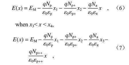
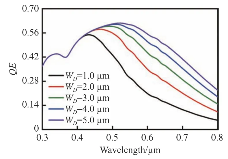
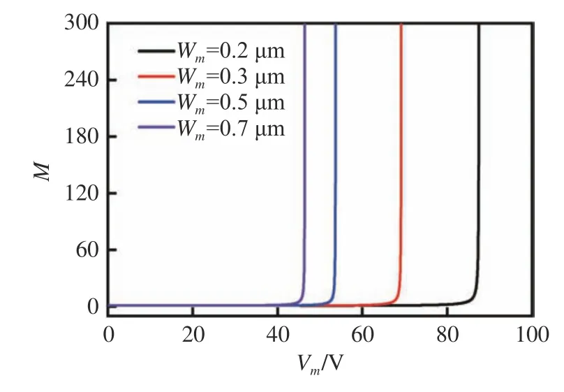
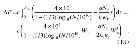
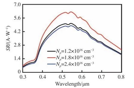
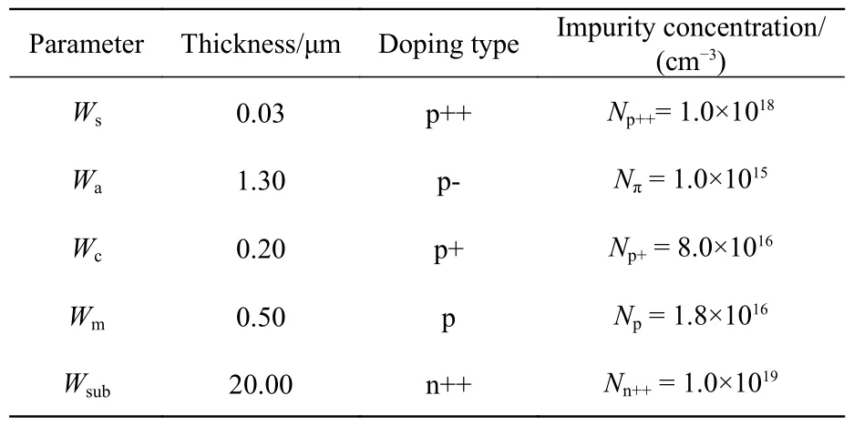
when 0 whenx1 whenx2 whereNp,Np+,NπandNp++are the doping concentrations of the multiplication layer,field control layer,absorption layer and surface non-depletion layer,respectively.By modulating the doping concentration and thickness of each layer,the electric field distribution and corresponding voltage in each layer can be designed and modulated;EMis the electric field strength at the position ofx=0 in Fig.2,which is also the maximum electric field strength in the device;εp,εp+,επandεp++represent the relative permittivity of the multiplication layer,field control layer,absorption layer and surface non-depletion layer.The relative permittivity of doped silicon[24]can be expressed as: N-type doped silicon: If the thickness and doping concentration of each layer are determined,according to the electric field distribution in the device defined by Equations(4)−(7),the voltageVapdon the Si-APD device in Fig.1 can be expressed as: whereVcandVaare the voltages on both sides of the field control layer and the absorption layer,respectively.IfEMreaches the maximum valueEbrduring the avalanche multiplication breakdown,the voltage applied across the device at this time is the avalanche breakdown voltageVbr-apd. Quantum efficiencyQEis the number of electron-hole pairs generated inside a semiconductor by a single incident photon[25],which is defined as: whereIphis the photocurrent,Poptis the incident light power,hνis the single-photon energy,andqis the charge of the electron.Assuming that all the carriers generated by the incident illumination of Si-APD under the action of working bias enter the depletion region,the quantum efficiencyQErelation can be expressed as: whereφis the probability that a single photon absorbed by the material excites a hole-electron pair;Ris the reflectivity of the silicon surface,αis the light absorption coefficient of the material,and the relation ofRandαon the wavelength is shown in Fig.3 (color online);WDis the depletion layer thickness.Equation (12) shows that the excitation probabilityφof photogenerated carriers is fixed,and under the action of incident light of a certain wavelength,the quantum efficiency of APD is mainly affected by the surface reflectivityRand the thickness of the depletion layerWD.For the convenience of calculation,assuming thatφ=100%,and all the excited hole-electron pairs can enter the depletion layer,the relation between the quantum efficiency of Si-APD blue light band and the thickness of the depletion layer is calculated by formula (12).The results are shown in Fig.4 (color online),that is,when the depletion layer thicknessesWDare 1.0 μm,2.0 μm,3.0 μm,4.0 μm and 5.0 μm,the corresponding peak quantum efficienciesQEpeakare about 55.03%,58.23%,59.83%,60.99% and 61.72%,and the corresponding incident wavelengthsλpeakare 0.43 μm,0.47 μm,0.49 μm,0.51 μm and 0.52 μm,respectively. Fig.3 The surface reflectance and absorption coefficient of the silicon vary with different incident wavelengthes图3 硅表面反射率及吸收系数随入射波长的变化情况 Fig.4 The relationship between quantum efficient and incident wavelength under different depletion layer thicknesses图4 不同入射波长的量子效率与耗尽层厚度的关系 The above calculation curve results show the variation of quantum efficiency with incident wavelength under different depletion layer thicknessWD.It can be seen from the figure that the quantum efficiency increases with the increase of the depletion layer thicknessWD.The analysis shows that with the increase of the incident wavelength,the corresponding absorption coefficientαdecreases.The increase in the thickness of the depletion layer can improve the light absorption rate of Si-APD,and correspondingly increase the number of photogenerated electron-hole pairs in the depletion layer.The peak quantum efficiencyQEpeakred-shifts with the increase of the corresponding incident wavelength and the thickness of the depletion layer.It can be found from the curve in the figure that under the excitation of a specific incident wavelength,theQEpeak of the Si-APD quantum efficiency does not increase with the increase of the thickness of the depletion layer.This is because the light absorption of the depletion layer to the incident wavelength is saturated,making the number of photogenerated carriers constant,for example,when the depletion layer thicknessWD≥2.0 μm,the quantum efficiency at the incident wavelength λ=0.45 μm is fixed atQE=57.58%. The photoresponsivitySRis a measure of the photoelectric conversion capability of the photodetector on the macroscopic scale,which is defined as the ratio of the photocurrentIphto the incident optical powerPopt,and the expression isSR=Iph/Popt.The relationship between optical responsivity and quantum efficiency is[26]: whereMis the gain coefficient.According to the quantum efficiencyQEdefined by Eq.(12),the above equation can be rewritten as: Assuming that the gain coefficientM=1 andφ=100%,the relationship between the optical responsivitySRin the visible light band and the thicknessWDof the depletion layer is calculated according to Eq.(14),as shown in Fig.5 (color online). Fig.5 The relationship between spectral response and incident wavelength under different depletion layer thicknesses图5 在不同耗尽层厚度下,光响应度与入射波长的关系 The curves in Fig.5 show that when the depletion layer thicknessWDare 1.0 μm,2.0 μm,3.0 μm,4.0 μm or 5.0 μm,the corresponding peak photoresponsivitySRpeakare about 0.196 A·W−1,0.226 A·W−1,0.246 A·W−1,0.261 A·W−1,or 0.272 A·W−1,and the corresponding incident wavelength λ are 0.44 μm,0.50 μm,0.52 μm,0.56 μm,or 0.57 μm,respectively,which are consistent with the incident wavelength corresponding to the peak quantum efficiency. The photocurrent gain is the most important characteristic of APD,and its underlying physical mechanism is the impact ionization effect of carriers,which is usually expressed by a multiplication factor.Assuming that the avalanche effect only occurs in the multiplication layer,the multiplication factorM(x)[27]defined by Eq.(15) shows that the avalanche multiplication is mainly depended on the width of the depletion layer,the electric field strength,the collision ionization coefficient of carriers,etc.In the case of electron-induced avalanches,the multiplication factorM(x)is: whereα(x) andβ(x) are the collisional ionization coefficients of electrons and holes,respectively,andWmis the thickness of the multiplication region.Chynoweths describes the effect of electric field strengthEon the collisional ionization of carriers as[28]: wherean,bn,apandbpare the experimental parameters of the collision ionization rate of electrons and holes,respectively,andE(x) is the electric field strength in the multiplication region,which is a function of the distancex.The numerical calculation in this paper adopts Lee’s experimental fitting coefficients[29]:an=3.8×106cm−1,bn=1.75×10⁶V·cm−1;ap=2.25×106cm−1,bp=3.26×10⁶V·cm−1. Consider the relationship among the thickness of the multiplication layer in the PN junction,the applied bias voltageVmon both sides of the multiplication layer,and the multiplication coefficientMunder a certain doping concentration.Assuming that the doping concentration of theN-type substrate isND=1.0×1019cm−3,and the doping concentration of theP-type multiplication layer isNA=1.0×1016cm−3,combined with Eqs.(1),(2),and (16),in order to simplify the calculation,perform the third-order Taylor expansion ofα(x) andβ(x),and substitute them into Eq.(15) to calculate the relationship between the applied bias voltageVmof the multiplication layer and the multiplication coefficientM,the result is shown in Fig.6 (color online). Fig.6 The relationship between the thickness of multiplication layer and multiplication factorM图6 倍增层厚度与倍增系数M 的关系 The curves in the above figure show thatMincreases sharply when the applied bias voltageVmon both sides of the multiplication layer increases to a specific value,and Equation (15) shows thatVmis close to or equal to the voltageVbr-mon both sides of the multiplication layer at the time of avalanche breakdown.Therefore,in order to obtain a higher gain for the APD,the applied bias voltageVapdacting on the device needs to approximate the avalanche breakdown voltageVbr-apdof the device.The curves in the figure shows that as the thickness of the multiplication layer increases,the voltage to obtain the same multiplication factor decreases.That is,at small multiplication layer thickness,the voltage needs to be increased so that the carriers have a higher ionization rate in order to obtain a higher gain.However,the increase of the thickness of the multiplication layer is affected by the doping concentration and the applied bias voltage at both ends of the PN junction,and the selection of the thickness is also based on the electric field distribution,which is related to the doping concentration,so the thickness of the multiplication layer needs to be comprehensively considered with its doping concentration. For silicon,the carrier energy is completely lost in the collisional ionization only when the electron energy isEele≥6.5 eV[30].From the perspective of energy,it is assumed that the collision ionization effect occurs only in the multiplier layer,the influence of field control layer on electron energy is not considered,and the hole electron recombination mechanism and scattering energy loss are ignored.It can be seen from formula (4),that let the carrier obtain energy under the action of the electric field of the multiplication layerΔEis: For the convenience of calculation,the critical breakdown electric field intensityEMis substituted into the above formula ΔE,and we have: The doping concentration of the substrate is set toNn++=1.0×1019cm−3,the doping concentration of the multiplication layerNpis 1.0×10¹⁵~1.0×1017cm−3,and the PN junction is set as a unilateral mutation junction.According to Eq.(18),the numerical relationship between the doping concentration and the carrier energyΔEunder different multiplication layer thicknesses was calculated,and the results are shown in Fig.7 (color online).When the thickness of the fixed multiplication layer isWm=0.5 μm,the curves in the figure show that when the doping concentrationsNpis 1.2×1016cm−3,1.8×1016cm−3or 2.4×1016cm−3,the energyΔEis 18.22 eV,18.39 eV or 18.26 eV,respectively.Therefore,when the doping concentration of the multiplication layer is 1.8×1016cm−3,the carriers obtain a higher energyΔE=18.39 eV in the multiplication layer,which can theoretically generate a higher gain coefficientM. Fig.7 Relationship between carrier energy ΔE and multiplication layer doping concentration图7 载流子获得能量ΔE 与倍增层掺杂浓度的关系 The doping concentration (Np+) and the thickness (Wc) of the field control layer are important for adjusting the electric field intensity between the multiplication layer and the absorption layer.The field control layer is located between the absorption layer and the multiplication layer,and reduces the tunneling probability of the device by reducing the electric field strength of the absorption layer.However,the thickness of the field control layer should not be too large.The reasons are as follows:when the applied bias voltage and the doping concentration of the field control layer are fixed,increasing the thickness of the field control layer will reduce the electric field strength of the absorption layer,and affect the drift velocity of photogenerated carriers in the absorption layer;if the thickness is too small,it will increase the electric field strength of the absorption layer,induce carrier ionization,and increase unnecessary noise current.According to Eq.(5),under the condition of ensuring the carrier saturation drift velocity,the appropriate doping concentration and thickness is beneficial to the modulation and transition of the electric field between the multiplication layer and the absorption layer.In general,compared with multiplication.a smaller thickness and a higher doping concentration should be chosen to ensure the least effect on the multiplication layer variation. Due to the absorption characteristics of Si material itself[31],the blue light band in the wavelength range of 0.4~ 0.5 μm has a high absorption coefficient (as shown in Fig.3),which leads to a shallow penetration depth of light in the blue light band,about 0.098~0.82 μm in silicon.In order to fully absorb the blue light by the absorption layer,the thickness of the absorption layerWa=1.3 μm is selected in combination with the relationship between the quantum efficiency and the thickness of the depletion layer shown in Fig.4.In silicon,when the electric field strengthE>1.0×10⁴V·cm−1,the velocity of electrons tend to the saturation drift velocity,that is,vs(Si)≈107cm·s−1.In order to keep the high bandwidth of the device,the carriers should move at the saturation velocity in the device.When the doping concentration and thickness of the multiplication layer and the field control layer are fixed (Wm=0.5 μm,Np=1.8×1016cm−3;Wc=0.2 μm,Np+=8.0×1016cm−3),and the mutation PN junction is close to breakdown,the field strength distribution of the absorption layer under different doping concentrations is drawn according to Eq.(6),as shown in Fig.8(color online).It can be seen from the figure that the field strength of the absorption layer gradually decreases with the increase of the doping concentration.When the doping concentration of the absorption layer isNπ=1.0×1016cm−3and 5.0×1015cm−3,the field strength has been exhausted before reaching the surface non-depletion region,and at this time,the blue-light excited carriers enter the absorption layer and are dominated by diffusion motion,which increases the carrier transit time and reduces the device bandwidth.WhenNπis1.0×1014cm−3,5.0×1014cm−3or 1.0×1015cm−3,respectively,the edge field strength of the absorption layer isE>104V·cm−1,the device is in the pull-through state,and the carriers drift at the saturation velocity in the whole device.Therefore,the doping concentration and thickness of the absorption layer should be selected so that the absorption layer have a good electric field distribution and the carriers move in this layer at a saturated drift velocity,and that the red and green light has a certain absorption rate at the same time. Fig.8 Field intensity distribution of the absorption layer under different doping concentrations图8 不同吸收层掺杂浓度下吸收层的场强分布 Assuming that the layers are uniformly doped,the incident light is absorbed only in the absorption layer,and under reverse bias voltage,the avalanche effect occurs only in the multiplication layer.Based on the relationship among the gain coefficient,the applied bias voltage and the thickness of the multiplication layer,the relationship among the quantum efficiency,the photoresponsivity and the thickness of the depletion layer,the selected parameters of each layer are shown in Table 1,whereWs,Wa,Wc,WmandWsubare the thicknesses of the surface nondepletion layer,absorption layer,field control layer,multiplication layer and substrate,respectively. Tab.1 Parameters of Si-APD layers表1 Si-APD 各层参数 The basic equations of semiconductor device operation include electrostatic equation,current density equation and continuity equation.The generation and recombination mechanism of carriers is the key to the performance of semiconductor photodetectors.In the two-dimensional simulation of the device characteristics of Si-APD,the diameter of the photosensitive surface of the Si-APD used in the calculation is 10 μm.In order to improve the accuracy of the calculation results,physical models such as Selberherr's ionization[32,33],Shockley-Read-Hall recombination[34, 35]and carrier mobility[36-38]are used in the calculation. According to the parameters in Table 1,when theVapdin the device is 0 V,0.5Vbr-apd,0.7Vbr-apdorVbr-apdrespectively (the correspondingVapdis 0 V,17.1 V,23.9 V,34.2 V),the field strength distribution inside the Si-APD as shown in Fig.9 (color online).It can be seen from the figure that the electric field strength inside the Si-APD increases with the increase of the bias voltageVapdapplied to the device.WhenVapdis small,the device is in a nonpull-through state,and the carriers begin to diffuse in the device.With the increase of the applied bias voltage,the device is pulled through as a whole,at this time,the carriers are dominated by drift motion.As the applied bias voltage is continuously increased,the carriers will eventually move in the device at the saturation drift velocity. Fig.9 The field strength distribution of Si-APD under different applied bias voltages图9 不同外加偏压下Si-APD 的场强分布 Generally,the surface of the semiconductor photodetector has a certain thickness of the surface heavily doped non-depletion layer (also act as an electrode layer),and the penetration depth of light in the blue light band in silicon is relatively small.When light passes through the non-depleted layer at the top of the device,most of the blue light energy is absorbed by this layer to generate hole-electron pairs,so it is necessary to optimize the thickness of the surface non-depleted layer.On the basis of the parameters in Table 1,the impurity concentration of the surface layer and the structural parameters of other doped layers are fixed,the incident light is vertically irradiated on the surface layer of the detector,and the spectral response curves of different surface non-depleted layer thicknesses are obtained whenR≠0,which are shown in Fig.10 (color online). Fig.10 Effect of thickness of surface layers of Si-APD on spectral responsivity图10 不同表面层厚度Si-APD 的光谱响应曲线 The curve in the figure shows the spectral responsivity under the applied bias voltage of 0.95Vbr-apd(M≈26) when the thickness of the surface non-depletion layer isWs=0.03 μm,0.06 μm and 0.10 μm.WhenWs=0.03 μm,the photoresponsivity of the blue bandSRis 3.71~6.08 A·W−1;whenWs=0.06 μm,the photoresponsivitySRof the blue band is 3.15~5.94 A·W−1;whenWs=0.10 μm,the photoresponsivitySRin the blue band is 2.57~5.75 A·W−1,indicating that the smaller the thickness of the surface non-depletion layer is,the smaller the inhibitory effect on the photoresponsivity of blue light will be.It is also found from the curve that the change ofWshas little effect on the optical responsivity of the device in the long wavelength band.The analysis shows that according to the transmission characteristics of light in the medium,the light absorption lossAsof the incident light in the surface non-depletion layer with a thickness ofWsis whereRis the surface reflectance,andαis the light absorption coefficient of Si.The drift current density formed by photogenerated carriers in the depletion region of widthWDis: For the fixed incident optical powerPoptin the visible light band,the first half of Eq.(20) represents the number of photons that penetrate to the edge of the depletion layer of the detector at a specific wavelength,and the second half represents the absorption rate of the incident photons by the depletion layer with a thickness ofWD.Ignoring the recombination mechanism of carriers,set the quantum efficiencyQE=100% in the depletion region.According to the material characteristics of Si,the intensity of long-band incident light absorbed by the material is small,so the light absorption loss generated by the surface non-depletion layer has little effect on the light energy transmitted to the depletion layer.Therefore,the long wave band light response is basically stable in the process of adjustingWs.However,on the short-wave side,the thickness of the surface non-depletion layer has a great influence on the optical responsivity. According to the calculation results in Fig.10 and the calculation results of the surface non-depletion layer thickness above,take the surface non-depletion layer thicknessWs=0.03 μm,the surface reflectivityR≠0,and other parameters are based on the data in Table 1 to obtain that whenVapd=0.95Vbr-apd,the photoresponsivity of Si-APD in the visible light band is shown in the red curve in Fig.11 (color online),and the corresponding photoresponsivitySRin the blue light band is divided into 3.72~6.08 A·W−1. Fig.11 Effect of doping concentration of multiplication layer on spectral responsivity图11 倍增层掺杂浓度对光响应度的影响 For comparison,when other parameters remain unchanged,the doping concentrations of the multiplication layerNPare calculated as 1.2×1016cm−3,2.4×1016cm−3(the corresponding breakdown voltageVbr-apdis 39.2 V and 30 V respectively).The photoresponsivity atVapd=0.95Vbr-apdare shown in the blue and black lines in Fig.11(color online).The corresponding photoresponsivity in the blue light bandSRare divided into 3.02~4.93 A·W−1and 2.83~4.68 A·W−1.In both cases,the photoresponsivity is lower than theSRvalue forNp=1.8×1016cm−3doping indicated by the red line. This phenomenon can be attributed to the fact that at this doping concentration,the carriers can gain higher energy in the multiplication layer (as shown in Fig.7),resulting in a greater photocurrent gain.Based on the above results,the basic epitaxial structure parameters of the Si photodetector were finally determined as shown in Table 2. Tab.2 Parameters of Si-APD layers表2 Si-APD 各层参数 Assuming that each layer is uniformly doped,the I-V relationship characteristics of the Si-APD in the dark environment can reflect the electrical parameters such as the avalanche breakdown voltageVbr-apdand the current gain coefficientMof the device.The I-V characteristic curves are calculated qualitatively according to the parameters in Table 2 and the current density equation defined in Equation (21).The current density magnitude is mainly influenced by the carrier transport behavior and is expressed in the numerical relationship as the sum of electron current density and hole current density,i.e.: whereJnis the electron current density,Jpis the hole current density,Jcondis the conduction current density,μnis the electron mobility,μpis the hole mobility,Dnis the electron diffusion coefficient,Dpis the hole diffusion coefficient,∇nand ∇pare the excess carrier concentration gradients.The curve in Fig.12 (color online) shows the calculated reverse current as a function of the applied bias voltageVapd.It can be seen from the figure that the magnitude of the current increases with the increase ofVapd,but the change trend of the current is different.According to different current formation mechanisms,it is s ummarized as parts (i)-(iv) in Fig.12. Fig.12 The dark current I-V curve of Si-APD图12 Si-APD 暗电流的 I-V 曲线 The dark current density of avalanche photodiode includes[39]recombination current densityJr,minority carrier diffusion current densityJdiff,carrier drift current densityJdrof depletion layer and avalanche current densityJm.The recombination current density is expressed asJr=qniWD/2τD.τD=1/Rec·Nis the carrier lifetime,Rec≈10−15cm3s−1is the indirect band gap semiconductor recombination coefficient[27],andNis the doping concentration.Jdiff=(qDpni2/LpND)+(qDnni2/LnNA),Dp=kTμp/qandDn=kTμn/qare the diffusion coefficient of hole and electron respectively,LpandLnare the diffusion length of hole and electron respectively.WhenT=300 K,kT/q=0.025 9 V,Dp=12.95 cm2·s−1,Dn=37.56 cm2·s−1.For simple calculation,combined with the doping concentration of π absorption layer,p+type field control layer and p type multiplication layer in the APD structure designed above,the three regions are regarded as p type silicon materials with doping concentrationand carrier life whereτsc(p),τsc(p+)andτsc(π)are the carrier lifetimes of the multiplication layer,the field control layer and the absorption layer,respectively. When the applied bias voltageVapdis small,the Si-APD current is dominated by the diffusion and recombination currents.Substituting the above data into equation (24) to calculate the diffusion and recombination currents of the device,the results correspond to part (i) in Fig.12. When increasing the applied bias voltageVapd,the number of carriers subjected to the internal electric field increases and the drift current accounts for the major part of the current.According to equation(21),the drift current density of the device is expressed asJdr=qnμnE+qpμpE,whereEis the electric field strength of the depletion layer defined by equations (4) to (7).Substituting the calculatedJdrinto the following equation,the result corresponds to part (ii) in Fig.12. If the applied bias voltageVapdcontinues to increase,the carriers collide and ionize under the action of strong electric field.The high-energy initial carriers collide with the internal lattice to produce secondary carriers,and then continue to collide with the lattice to produce new carriers to form avalanche current densityJm=αnJn+αpJp,JnandJpare electron and hole current densities,αn,αpare the ionization coefficient of electrons and holes,respectively.The collision effect continues under the working bias voltage and the number of carriers is doubled.Assuming that the avalanche effect only occurs in the multiplication layer,the avalanche dark currentIdgenerated in the multiplication layer with a thickness ofWmcan be expressed as: As shown in part (iii) of Fig.12. Generally,the gain coefficientMof the device can be obtained from the following empirical relation whereIdis the dark current generated based on the impact ionization of the carriers,Id0is the initial dark current,the constantnis affected by the device structure,doping distribution and other factors,usually thenof the Si material is 1.5−4.0.When the applied bias voltageVapdis close to the avalanche breakdown voltageVbr-apd,the current will increase with the sharp increase of the multiplication factorM,as shown in the area (iv) in Fig.12. The dark current I-V curve in Fig.12 shows that when the APD device is at a low applied bias voltage,the diffusion current accounts for most of the total current;after that,the internal electric field strength will increase with the increase ofVapd,and the width of the depletion region will increase too.More carriers enter the depletion region to form a drift current under the action of the electric field,which becomes the main part of the total current;whenVapdcontinues to increase,due to the impact ionization of carriers,there will be a current gain phenomenon,but the effect is not obvious;ifVapdis close to the device avalanche breakdown voltageVbr-apd,and there will be a sharp increase in current. By comparing the variation trend of current with voltage in parts (iii) and (iv),it can be found that APD can produce a higher current gainMwhen the bias voltage is higher than the avalanche breakdown voltage.According to the analysis,the ionization rate of the carrier is an important indicator to measure the avalanche multiplication effect,which is closely related to the electric field strength associated with the device bias voltage[40],and the ionization rate increases with the increase of the bias voltage.Taking the carriers in the multiplication layer as an example,the impact ionization rate distributions of electrons and holes under different bias voltages are calculated according to Equation(16),Lee's carrier ionization parameter and the electric field distribution of Equation (4),Figs.13 (a)and 13(b) (color online) clearly show that the collision ionization coefficient increases with the increase of the voltageVmon both sides of the multiplication layer,so whenVapdapproachesVbr-apd,there will be a high current gain,and the electron gain is dominant. Fig.13 (a) Electron ionization coefficients in the multiplication layer under different bias voltages;(b)hole ionization coefficients in the multiplication layer under different bias voltages.图13 (a) 不同倍增层偏压下倍增层内电子离化系数;(b)不同倍增层偏压下倍增层内空穴离化系数 In order to meet the urgent demand for blue light high response photodetectors in optical communication systems,a SACM type Si-APD structure with interchangeable positions of absorption layer and multiplication layer is designed and the relationship between multiplication layer thickness and device gain,absorption layer doping concentration and absorption layer field strength distribution,external bias and internal field strength distribution,surface non-depletion layer thickness and spectral response,and multiplication layer concentration and spectral response are studied.After comprehensive consideration,the structural parameters of the device are selected as follows:the thickness of the surface non-depletion layer is 0.03 μm,the doping concentration is 1.0×1018cm−3;the thickness of absorption layer is 1.3 μm,the doping concentration is 1.0×1015cm−3;the thickness of field control layer is 0.2 μm,the doping concentration is 8.0×1016cm−3;the thickness of multiplication layer is 0.5 μm,the doping concentration is 1.8×1016cm−3.The device has a low breakdown voltageVbr-apd=34.2 V.WhenVapd=0.95Vbr-apd,it has a high optical responsivity of 3.72~ 6.08 A·W−1in the blue band.The results of this paper have a certain reference value for the preparation of actual devices. ——中文对照版—— 随着短波长可见光光源(如蓝光LED、蓝光半导体激光器等)的发展和广泛应用,短波长可见光高效探测技术的应用越来越广泛。尤其是可见光通信技术[1]、生物医学工程、水下光通信[2]等领域的快速发展,迫切需要具有高带宽、高增益、宽光谱、高光响应的可见光探测器[3]。白光LED 是可见光通信的重要光源[4],目前常用的白光LED 主要有荧光型白光LED(通过蓝光LED激发荧光粉混合形成白光[5])、红蓝绿型白光LED(RGB-LED)[6],上述两种白光LED,蓝光都是主要的工作波段,因此具有蓝光高响应的光电探测器对进一步促进照明通讯一体化的发展应用具有重要意义[7]。目前常用的光电探测器主要为:PIN 光电二极管(PIN-PD)、光电倍增管(Photo Multiplier Tube,PMT)和雪崩光电二极管(Avalanche Photodiode,APD)。然而,PIN 光响应度低、探测距离短,对光源功率要求高,限制了其在可见光通信中的进一步应用[8]。光电倍增管(PMT)可以探测短波长,然而电压高、对磁场敏感等缺点限制了其在可见光通信方面的应用[9]。雪崩光电探测器(APD)是一种具有较高的内部增益和高光响应度的半导体探测器[10],并且没有PMT 的上述缺点,在可见光探测器的研究中引起了广泛关注。 硅(Si)对于380~ 1100 nm 波段的入射光均有吸收能力,是制备宽光谱探测器的良好材料[11],且Si 半导体器件制备工艺成熟[12],同时硅材料中电子与空穴的碰撞电离率比值高、隧道电流低[13],使得硅基雪崩光电二极管(Si -APD)具有增益高,噪声低,稳定性好等优点。然而由于蓝光在硅中的高吸收系数特性使得蓝光在硅中的透入深度较低,大部分的光生载流子位于浅表层,易导致部分载流子在浅表面复合,进入吸收层的光生载流子数量较少,降低了蓝光波段的光电转换效率,这给蓝光高响应度的Si-APD 的器件设计和制备带来较大难度。为了提高硅对蓝光的探测效率,改善Si-APD 在蓝光波段的性能,研究人员进行了相关的研究:2010 年,Excelitas 公司的Catherine M.Pepin 等人通过在外延片上“埋结”,制备了一种紫外增强型Si 基APD,该器件的雪崩击穿电压为400 V,在430 nm 波长处的响应度为39 A/W(M=150)[14]。2015 年,Othman 等人通过CMOS工艺将Si 基APD 高度集成,雪崩击穿电压为10 V,在405 nm 波长处的增益为100[15]。同年,王旭东等人基于吸收场控倍增分离(SACM)型Si-APD(n-p-p+-p-p+型掺杂结构,光从N 型层表面入射)优化了器件结构参数,同时在器件表面设计了折射率高低交替分布的增透膜结构,优化后器件的峰值响应波长为406 nm,雪崩击穿电压为105.9 V,峰值波长处的光响应度为250 A/W[16]。2015 年,霍林章等人提出了一种深槽隔离结构的SiPM 探测器,提高了在蓝紫光区(360~420 nm)的探测效率,该器件的击穿电压约为90V[17]。2019年,鲁欢欢等人设计了一种SAM 型Si-APD,该器件的倍增层更靠近光敏层,能够有效降低光生载流子的复合损耗,该器件的击穿电压约为50 V,450 nm 处的光响应度为31.1 A/W[18]。上述研究改善了所设计的Si-APD 器件的蓝光探测效率。随着需求的日益增长,有必要对Si-APD 器件作进一步研究,以提高其蓝光探测性能。传统的Si-APD 器件雪崩击穿电压Vbr较高(150~500 V),而高的雪崩击穿电压使得器件功率变大,稳定性变差。为获得在蓝光波段的硅基APD 器件的高蓝光响应度和较低的雪崩击穿电压,本文在传统的Si-APD 结构基础上,根据光激发载流子的输运特征,优化设计了一种吸收层与雪崩层位置互换的结构,并对结构在蓝光波段进行了优化。对器件倍增层的掺杂浓度及厚度与雪崩击穿电压和光谱响应度的关系进行了研究。本文为设计与制备实际高蓝光响应度硅基雪崩光电探测器芯片提供参考。 根据对Si 吸收可见光特性(本文所使用的Si 材料参数来自于Schinke 等人的实验测量值[19])和Si 雪崩光探测器工作原理的分析,本文采用一种SACM 型器件结构,即:吸收层和倍增层分离,并在二者之间加入场控层,将倍增层后置[20-21]。SACM 型Si-APD 基本外延结构如图1(彩图见期刊电子版)所示。器件自上而下分别为p++型重掺杂表面非耗尽层、π 型吸收层、p+场控层、p 型倍增层以及n++型衬底,光从p++非耗尽层表面入射。吸收层可吸收波长为0.3~1.1 μm的入射光,覆盖可见光波段;场控层用于调制器件中倍增层与吸收层的电场,实现吸收层的低电场强度和倍增层的高电场强度良好过渡,在保证光生载流子能输运到雪崩层的前提下,抑制噪声载流子[22];倍增层用于实现初始光生载流子的数量增益;表面非耗尽层和重掺杂衬底兼具导电电极作用。当外加偏压足够高时,器件将处于拉通状态,即耗尽区从PN 结直到表面非耗尽层,在保证倍增层的雪崩击穿的同时,也保证吸收层电场足够高,使光生载流子能够达到饱和漂移速度从而运动到倍增层。 PN 结耗尽层的电场分布可以表示为: 式中,q为单电荷量,Nm为杂质浓度,εm为掺杂材料的相对介电常数,ε0为真空介电常数,EM为PN 结内最大电场强度,EM由倍增层两侧的掺杂浓度及外加偏压Vm决定,表示为, 其中ND为施主杂质浓度,NA为受主杂质浓度,Vbi为倍增层的内建电势,Vm为倍增区两侧的电压,表示为: 式中,K为玻尔兹曼常数,T为开尔文温度(T=300 K),ni为本征载流子浓度(ni=1.02×1010cm−3[23])。 根据公式(1),推导求出图2(彩图见期刊电子版)中器件各层电场表达式(本文中没有考虑同质结因掺杂浓度不同产生的内建电势)。 当0 当x1 当x2 当x3 式中,Np、Np+、Nπ和Np++分别为倍增层、场控层、吸收层和表面非耗尽层的掺杂浓度,通过调整各层掺杂浓度和厚度,可以设计和调整各层中的电场分布及相应的电压;Em为图2 中,x=0 位置处的电场强度,也为器件中的电场强度最大值;εp、εp+、επ与εp++表示倍增层、场控层、吸收层与表面非耗尽层的相对介电常数。掺杂硅的相对介电常数[24]表达式分别为: N 型掺杂硅: P 型掺杂硅: 如果确定了各层厚度和掺杂浓度,根据公式(4)−(7)定义的器件内部电场分布,图1 中Si-APD 器件上的电压Vapd的表达式为: Vc和Va分别为场控层、吸收层两侧的电压。如果EM达到雪崩倍增击穿时的最大值Ebr,那么,此时器件两端所加的电压则为雪崩击穿电压Vbr-apd。 量子效率QE为单入射光子在半导体内部产生电子-空穴对的数目[25],定义式为: 式中,Iph表示光电流,Popt表示入射光功率,hν为单光子能量,q为电子的电荷量。假设Si-APD 在工作偏压作用下入射光照产生的载流子全部进入耗尽区,量子效率QE关系式可表达为: 式中,φ为被材料吸收的单光子激发空穴-电子对的概率;R为硅表面反射率,α为材料的光吸收系数,R、α对波长的依赖关系如图3(彩图见期刊电子版)所示;WD为耗尽层厚度。式(12)表明,光生载流子的激发概率φ固定,在一定波长的入射光作用下,APD 的量子效率主要受表面反射率R与耗尽层厚度WD的影响。为计算方便,假设φ=100%,且激发空穴-电子对都可以进入耗尽层,通过式(12)计算得出Si-APD 蓝光波段的量子效率与耗尽层厚度的关系,结果如图4(彩图见期刊电子版)所示。图4 中曲线展示了耗尽层厚度WD分别为1.0、2.0、3.0、4.0 与5.0 μm 时,所对应的峰值量子效率QEpeak分别为55.03%、58.23%、59.83%、60.99%和61.72%,相应的入射波长λpeak分别为0.43 μm、0.47 μm、0.49 μm、0.51 μm 和0.52 μm。 图4 给出了不同耗尽层厚度WD时量子效率随入射波长的变化情况。从图中可以看出:量子效率随耗尽层厚度WD的增加而提高。分析认为,随着入射波长的增加,相应的吸收系数α减小,而耗尽层厚度增大可提高Si-APD 的光吸收率,相应地增加耗尽层内光生电子-空穴对的数量,峰值量子效率QEpeak随相应入射波长、耗尽层厚度的增加而红移。通过图中曲线可以发现,Si-APD 在特定入射波长的激励下,量子效率QE峰值不随耗尽层厚度的增加而提高,这是由于耗尽层对该入射波长的光吸收饱和,使光生载流子数量恒定,因此出现量子效率稳定现象,例如当耗尽层厚度WD≥2.0 μm 时,入射波长λ=0.45 μm 的量子效率固定为QE=57.58%。 光响应度SR是衡量光电探测器在宏观上的光电转换的能力,定义为光电流Iph与入射光功率Popt的比值,表达式为SR=Iph/Popt。光响应度与量子效率关系式为[26]: 式中,M为增益系数。根据式(12)定义的量子效率QE,上式改写为: 假设增益系数M=1,φ=100%,根据式(14)计算得到可见光波段光响应度SR随耗尽层厚度WD的变化关系,如图5 所示。 图5 中曲线表明,耗尽层厚度WD分别为1.0、2.0、3.0、4.0 与5.0 μm 时,所对应的峰值光响应度SR分别约为0.196、0.226、0.246、0.261和0.272 A·W−1,相应的入射波长λ分别为0.44、0.50、0.52、0.56 和0.57 μm,与峰值量子效率所对应的入射波长相一致。 光电流增益是APD 最重要的特性,其根本物理机制是载流子的碰撞电离效应,通常用倍增系数表示。假设雪崩效应仅发生在倍增层,则在电子引发的雪崩情况下,倍增系数M(x)如式(15)所示[27]。由式(15)可知,雪崩倍增主要由耗尽层宽度、电场强度、载流子的碰撞离化系数等决定。 式中,α(x)和β(x)分别为电子和空穴的碰撞离化系数,Wm为倍增区厚度,Chynoweths 描述了电场强度E对载流子碰撞离化的影响,关系式为[28]: 式中,an,bn,ap,bp分别为电子和空穴的碰撞离化率的实验参数,E(x) 是倍增区中电场强度,为距离x的函数。本文的数值计算采用Lee 的实验拟合系数[29]:an=3.8×106cm−1,bn=1.75×10⁶V·cm−1;ap=2.25×106cm−1,bp=3.26×10⁶V·cm−1。 考虑在一定掺杂浓度下,PN 结内倍增层的厚度、倍增层两侧的外加偏压Vm及倍增系数M三者之间的关系。假设N型衬底掺杂浓度为ND=1.0×1019cm−3,P型倍增层掺杂浓度为NA=1.0×1016cm−3,结合公式(1)、(2)、(16),为简化运算,将α(x) 和β(x) 进行3 阶泰勒展开,代入式(15)中,计算倍增层外加偏压Vm与倍增系数M的关系,结果如图6(彩图见期刊电子版)所示。 图中曲线表明当倍增层两侧的外加偏压Vm增加至特定值时,M急剧增加,公式(15)表明此时Vm大小接近或等于雪崩击穿时倍增层两侧的电压Vbr-m,因此,为了使APD 获得较高增益,作用在器件的外加偏压Vapd大小需近似于器件的雪崩击穿电压Vbr-apd。图中曲线表明随着倍增层厚度的增加,获得相同倍增系数时的电压降低。即,在小的倍增层厚度下,需要提高电压,使载流子具有更高的电离率,才能获得较高的增益。但是倍增层厚度的增加受掺杂浓度和PN 结两端外加偏压的影响,其厚度的选择还要依据电场分布选择,而电场分布又与掺杂浓度相关,因此倍增层的厚度需要与其掺杂浓度综合考虑。 对于硅,仅当电子能量Eele≥6.5 eV,载流子能量才完全损耗在碰撞电离过程中[30],从能量角度分析,假设仅在倍增层发生碰撞电离效应,不考虑场控层对电子能量的影响,忽略空穴-电子复合机制及散射能量损耗,通过公式(4)可知,设载流子在倍增层的电场作用下获得能量ΔE为: 为简便计算,将PN 突变结击穿临近电场Em代入上式整理得ΔE: 设定衬底的掺杂浓度Nn++=1.0×1019cm−3,倍增层的掺杂浓度Np为1.0×10¹⁵~1.0×1017cm−3,PN结设为单边突变结,根据公式(18)计算不同倍增层厚度下掺杂浓度与载流子获得能量ΔE的数值关系,结果如图7 所示。当倍增层厚度Wm固定为0.5 μm 时,由图5 曲线可知,掺杂浓度Np分别为1.2×10¹⁶、1.8×10¹⁶与2.4×1016cm−3时,能量ΔE分别为18.22、18.39 与18.26 eV。因此,当倍增层掺杂浓度为1.8×1016cm−3时,载流子在倍增层获得较高能量ΔE=18.39 eV,理论上可产生较高的增益系数M。 场控层的掺杂浓度(Np+)和厚度(Wc)是调节倍增层与吸收层电场过渡的重要参数,场控层位于吸收层与倍增层之间,通过降低吸收层的电场强度,减少器件的隧穿几率。然而场控层厚度不宜过大,原因如下:当外加偏压与场控层掺杂浓度固定时,增加场控层厚度会将减小吸收层的电场强度,会影响吸收层光生载流子的漂移速度;而厚度过小,又会增加吸收层电场强度,诱发载流子电离,增加不必要的噪声电流。根据公式(5),在保证载流子饱和漂移速度下,选择合适的掺杂浓度和厚度,有利于倍增层和吸收层之间电场的调节和过渡。一般地,选择比倍增层小的厚度和比倍增层高的掺杂浓度,可以保证对倍增层变化的影响最小。 由于Si 材料自身的吸收特性[31],对波长为0.4~ 0.5 μm 的蓝光波段具有较高的吸收系数(如图3 所示),导致蓝光波段的光在硅中的穿透深度较浅,约为0.098~0.82 μm。为了使蓝光被吸收层充分吸收,结合图4 所示的量子效率与耗尽层厚度的关系,选取吸收层厚度Wa=1.3 μm。在硅中,当电场强度E>1.0×10⁴V·cm−1时,电子会趋于饱和漂移速度,vs(Si)≈107cm·s−1。为了使器件保持较高的带宽,载流子在器件中应以饱和速度运动。倍增层、场控层的掺杂浓度和厚度固定时(Wm=0.5 μm,Np=1.8×1016cm-3;Wc=0.2 μm,Np+=8.0×1016cm−3),当突变PN 结临近击穿时,根据式(6)绘制了不同掺杂浓度下吸收层的场强分布,如图8(彩图见期刊电子版)所示。从图中可以看出,吸收层的场强随着掺杂浓度的增加逐渐减小,当吸收层的掺杂浓度为Nπ=1.0×1016cm−3和5.0×1015cm−3时,场强在到达表面非耗尽区以前已经耗尽,此时蓝光激发的载流子进入吸收层以扩散运动为主,增加了载流子的渡越时间,降低了器件带宽。当Nπ分别为:1.0×1014cm−3、5.0×1014cm−3和1.0×1015cm−3时,吸收层的边缘场强E>104V·cm−1,器件处于拉通工作状态,载流子在整个器件中以饱和速度漂移运动。所以吸收层的掺杂浓度和厚度选取需保证吸收层内载流子有良好的电场分布,保证载流子的饱和漂移速度,同时还要满足红绿光有一定的吸收率。 假设各层掺杂均匀,入射光仅在吸收层被吸收,在反偏电压下,雪崩效应只发生在倍增层。基于上文关于增益系数与外加偏压、倍增层厚度的关系、量子效率及光响应度与耗尽层厚度的关系,选取的各层的参数如表1 所示,其中Ws、Wa、Wc、Wm和Wsub分别为表面非耗尽层、吸收层、场控层、倍增层和衬底的厚度。 描述半导体器件工作的基本方程有:静电方程、电流密度方程和连续性方程。载流子的产生与复合机制是影响半导体光电探测器性能的关键。对Si-APD 的器件特性进行二维模拟,计算采用的Si-APD 的光敏面直径为10 μm,为了提高计算结果的准确性,计算过程中采用了Selberherr's离化[32-33]、Shockley-Read-Hall 复合[34-35]及载流子迁移率[36-38]等物理模型。 根据表1 中的参数,研究了器件中Vapd分别为:0 V、0.5Vbr-apd、0.7Vbr-apd、Vbr-apd(所对应的Vapd分别为:0 V、17.1 V、23.9 V、34.2 V),Si-APD 内部的场强分布,如图9(彩图见期刊电子版)所示。从图中可以看出,Si-APD 内部的电场强度随着器件外加偏压Vapd的增加而提高。当Vapd较小时,器件处于非拉通工作状态,载流子在器件中,开始以扩散运动为主,随着外加偏压的增加,器件整体被拉通,此时载流子以漂移运动为主,随着外加偏压的不断增加,载流子最终将以饱和漂移速度在器件中运动。 通常半导体光电探测器表面具有一定厚度的表面重掺杂非耗尽层(兼作电极层),蓝光波段的光在硅中的穿透深度较浅,当光经过器件顶部的非耗尽层时,大部分蓝光能量被该层吸收产生空穴—电子对,因此有必要对表面非耗尽层的厚度进行优化。在表1 参数基础上,固定表面层的杂质浓度及其它掺杂层的结构参数,入射光垂直照射在探测器表面层,得到R≠0 时,不同表面非耗尽层厚度的光谱响应曲线,结果如图10(彩图见期刊电子版)所示。图中曲线展示了当表面非耗尽层厚度Ws分别为0.03、0.06 和0.10 μm 时,外加偏压为0.95Vbr-apd(M≈26)下的光谱响应度,其中当Ws=0.03 μm 时蓝光波段的光响应度SR为3.71~ 6.08 A·W−1;当Ws=0.06 μm 时蓝光波段的光响应度为SR为3.15~5.94 A·W−1;当Ws=0.10 μm时蓝光波段光响应度为SR为2.57~5.75 A·W−1,表明表面非耗尽层越薄,对蓝光光响应度的抑制作用会越小。通过曲线也发现,Ws的变化对器件在长波段入射光的光响应度的影响较小,分析认为根据光在介质中的传输特性,入射光在厚度为Ws的表面非耗尽层光吸收损耗As为: 式中,R为表面反射率,α为Si 的光吸收系数。宽度为WD的耗尽区内光生载流子形成的漂移电流密度为: 可见光波段入射光功率Popt固定,公式(20)的前半部分表示特定波长光透射至探测器的耗尽层边缘的光子数量,后半部分表征厚度为WD的耗尽层对入射光子的吸收率,忽略载流子的复合机制,设耗尽区量子效率QE=100%。根据Si 的材料特性可知,长波段入射光被材料吸收的强度较小,因此表面非耗尽层产生的光吸收损耗对透射至耗尽层的光能量影响较小,因此调节Ws的过程中长波段光响应度基本稳定。但在短波一侧,表面非耗尽层厚度对光响应度有较大的影响。 根据图10 的计算结果,结合上面非表面耗尽层厚度计算结果,取表面非耗尽层厚度Ws=0.03 μm,表面反射率R≠0,其它参数依据表1 中数据,得到Vapd=0.95Vbr-apd时,Si-APD 在可见光波段的光响应度如图11(彩图见期刊电子版)红色曲线所示,所对应的蓝光波段的光响应度分为SR=3.72~6.08 A·W−1。 作为比较,在其他参数不变的情况下,还分别计算了倍增层掺杂浓度Np分别为1.2×1016cm−3、2.4×1016cm−3(所对应的击穿电压Vbr-apd分别为39.2 V、30 V),Vapd=0.95Vbr-apd时的光响应度,如图11 中蓝线和黑线所示,所对应的蓝光波段的光响应度SR分别为3.02~4.93 A·W−1、2.83~4.68 A·W−1。这两种情况下,光响应度均低于红线所示的Np=1.8×1016cm−3掺杂时的SR值。 这种现象可以归因于在该掺杂浓度下,载流子在倍增层可以获得更高的能量(如图7 所示),产生更大的光电流增益。根据上述的研究结果,最终确定Si 光探测器的基本外延结构参数如表2 所示。 假定每一层都是均匀掺杂的,Si-APD 在暗环境中的I-V 关系特性可以反映器件的雪崩击穿电压Vbr-apd、电流增益系数M等电学参数。根据表2 中参数及公式(21)定义的电流密度方程定性计算I-V 特性曲线。电流密度大小主要受载流子输运行为的影响,在数值关系上表示为电子电流密度和空穴电流密度之和,即: 式中Jn为电子电流密度,Jp为空穴电流密度,Jcond为传导电流密度,μn为电子迁移率,μp为空穴迁移率,Dn为电子扩散系数,Dp为空穴扩散系数,∇n、∇p为过剩载流子浓度梯度。图12 中曲线展示了计算得到的反向电流与外加偏压Vapd的变化关系。从图中可以看出电流大小随Vapd的增加而不断提高,但电流的变化趋势不同,根据不同的电流形成机理,总结为图12 中(i)−(iv)部分。 雪崩光电二极管的暗电流密度包括[39]复合电流密度Jr,少子扩散电流密度Jdiff,耗尽层的载流子漂移电流密度Jdr与雪崩电流密度Jm。复合电流密度表示为Jr=qniWD/2τD。τD=1/Rec·N,为载流子寿命,Rec≈10−15cm3s−1,为间接带隙半导体复合系数[27],N为掺杂浓度。Jdiff=(qDpni2/LpND) +(qDnni2/LnNA),Dp=kTμp/q与Dn=kTμn/q分别为空穴与电子扩散系数,Lp和Ln分别为空穴与电子的扩散长度。当T=300 K 时,kT/q=0.025 9 V,Dp=12.95 cm2·s−1,Dn=37.56 cm2·s−1。为简便计算,结合上文设计的APD 结构中π 吸收层、p+型场控层与p 型倍增层的掺杂浓度,将该3 个区域视为掺杂浓度、载流子寿命的P 型硅材料: τsc(p),τsc(p+)与τsc(π)分别为倍增层、场控层与吸收层的载流子寿命。 当外加偏压Vapd较小时,Si-APD 电流以扩散电流和复合电流为主。将上述数据代式(24)计算器件的扩散与复合电流,结果对应于图12 的(i)部分。 增加外加偏压Vapd,受内部电场作用的载流子数量增多,漂移电流为电流的主要部分,根据式(21),器件的漂移电流密度表示为:Jdr=qnμnE+qpμpE,其中E为式(4)~(7)定义的耗尽层电场强度,将计算结果Jdr代入下式(25),结果对应于图12 中(ii)部分。 若外加偏压Vapd持续增加,载流子在强电场作用下发生碰撞电离,高能初始载流子撞击内部晶格产生次生载流子,之后继续碰撞晶格产生新的载流子,形成雪崩电流密度Jm=(αnJn+αpJp),Jn与Jp为电子与空穴电流密度,αn、αp分别为电子和空穴的离化系数。该碰撞效应在工作偏压下持续进行,载流子数量倍增,假设雪崩效应仅在倍增层内发生,则厚度为Wm的倍增层内产生的雪崩暗电流Id可以表示为: 如图12 的第(iii)部分所示。 通常,器件的增益系数M可根据经验关系式(27)得出 式中,Id为基于载流子激发碰撞电离作用下产生的电流,Id0为初始暗电流,常量n大小受器件结构、掺杂分布等因素影响,通常Si 材料的n为1.5~4.0。当外加偏压Vapd接近雪崩击穿电压Vbr-apd时,则此时电流会随倍增因子M急剧增加而提高,如图12 中区域(iv)所示。 图12 的暗电流I-V 关系曲线表明:APD 器件处于低外加偏压时,扩散电流占总电流的主要部分;之后内部电场强度随Vapd增加而提高,耗尽区宽度增大,更多的载流子进入耗尽区,在电场作用下形成漂移电流,其成为总电流的主要部分;当Vapd持续增加,由于载流子碰撞电离作用,出现电流增益现象但效果不明显;若Vapd接近器件雪崩击穿电压Vbr-apd,则出现电流急剧增加现象。 通过对比(iii)与(iv)部分中的电流随电压的变化趋势发现,APD 处于相对雪崩击穿电压较高的偏压时可产生较高的电流增益M。分析认为载流子的离化率是衡量雪崩倍增效应的重要指标,其与器件偏压相关联的电场强度联系紧密[40],离化率随偏压提高而增大。以在倍增层内的电子为例,根据(16)式并按照Lee的载流子电离参数与(4)式的电场分布计算电子、空穴在不同偏压下的碰撞电离率分布,图13(a)和图13(b)(彩图见期刊电子版)清楚表明碰撞离化系数随倍增层两侧电压Vm的增加而提高,因此在Vapd接近Vbr-apd时会出现电流高增益现象,并且以电子增益为主。 为了解决光通信系统对蓝光高响应光电探测器的迫切需求,本文设计了一种吸收层与倍增层互换位置SACM 型Si-APD 结构,研究了倍增层厚度与器件增益、吸收层掺杂浓度与吸收层场强分布、外加偏压与器件内部场强分布、表面非耗尽层厚度与光谱响应度以及倍增层浓度与光谱响应的关系,综合考虑,选取器件的结构参数为:表面非耗尽层厚度为0.03 μm,掺杂浓度1.0×1018cm−3;吸收层厚度为1.3 μm,掺杂浓度为1.0×1015cm−3;场控层厚度为0.2 μm,掺杂浓度8.0×1016cm−3;倍增层厚度为0.5 μm,掺杂浓度为1.8×1016cm−3。该器件具有较低的击穿电压Vbr-apd=34.2 V,当Vapd=0.95Vbr-apd在蓝光波段有较高的光响应度SR=3.72~6.08 A·W−1。本文的研究结果对实际器件的制备具有一定参考价值。



2.3 Quantum efficiency and photoresponsivity




2.4 Effect of multiplication layer parameters on gain




2.5 Influence of field control layer
2.6 Design of absorption layer

2.7 Si-APD initial structural parameters

3 Si-APD numerical calculation
3.1 The relationship between the field strength distribution of Si-APD and the applied bias voltage

3.2 Further optimization of the thickness of non-depletion layer on the surface


3.3 Effect of doping concentration of multiplication layer on optical responsivity
3.4 I-V characteristics of Si-APD dark current


4 Conclusion
1 引言
2 器件外延结构设计
2.1 SACM 型Si-APD
2.2 Si-APD 电场分布


2.3 量子效率与光响应度


2.4 倍增层参数对增益的影响


2.5 场控层的影响
2.6 吸收层设计
2.7 Si-APD 初始结构参数
3 Si-APD 数值计算
3.1 Si-APD 的场强分布与外加偏压的关系
3.2 表面非耗尽层厚度进一步优化设计


3.3 倍增层的掺杂浓度对光响应度的影响
3.4 Si-APD 暗电流的I-V 特性


4 结论
