Synergistic effects of total ionizing dose and radiated electromagnetic interference on analog-to-digital converter
2022-05-12PingWuLinWenZhiQianXuYunShengJiangQiGuoCuiMeng
Ping Wu· Lin Wen · Zhi-Qian Xu · Yun-Sheng Jiang · Qi Guo ·Cui Meng
Abstract The influence of combined total ionization dose(TID)and radiated electromagnetic interference(EMI)in a commercial analog-to-digital converter (ADC) was studied. The degradation of the direct-current response, the static parameters, and the dynamic parameters caused by the TID and EMI separately and synergistically is presented. The experimental results demonstrate that the increase in TID intensifies data error and the signal-tonoise ratio(SNR)degradation caused by radiated EMI.The cumulative distribution function of EMI failure with respect to data error and SNR with different TIDs was extracted. The decreasing trend of the threshold was acquired with a small sample size of five for each TID group. The result indicates that the ADC is more sensitive in a compound radiation environment.
Keywords Integrated circuit · Total ionizing dose ·Electromagnetic radiation · Synergistic effect · Combined environment
1 Introduction
Laser inertial confinement fusion (ICF) is a potential research focus for controlled thermonuclear fusion. However, a harsh transient ionizing radiation and electromagnetic environment is generated at the moment the lasers impinge on the pellet, as shown in Fig. 1. Although shielding measures are taken to minimize the influence of electromagnetic interference (EMI) on physical diagnostic devices, the high-dose-rate γ-ray could still penetrate the shield and induce a system-generated electromagnetic pulse inside the enclosure of the equipment[1].Therefore,the circuit components of diagnostic devices inside the shielded enclosure face a huge threat from both γ-ray and electromagnetic radiation.
Such phenomena as data interference and functional malfunction of diagnostic devices inside the ICF chamber have been reported [2-4]. Because of the harsh operating environment, the reliability of diagnostic devices and the credibility of physical data should be reappraised.The total dose effect of ionizing radiation has a degrading effect on the performance and reliability of electronic equipment,including electromagnetic susceptibility [5, 6]. The synergistic effect of the γ-ray and electromagnetic field on pacemakers was first studied around 1980. The result indicates that linear accelerators and betatrons should be used with extreme caution in the treatment of patients with pacemakers implanted [7, 8]. Some classical integrated circuit (IC) technologies, including complementary metaloxide-semiconductor inverters and bipolar junction transistors, have been investigated since 2010 [9-13]. Zhang studied the synergistic effect of the total ionization dose(TID) with an additional magnetic field on magnetoresistive random-access memory.Less damage was found in the synergistic test because of electron drift in the oxide [11].Vargas et al. established a platform for single-event upset,TID, and both conducted and radiated EMI [12-14]. Current consumption, fault occurrence, and susceptibility against IC voltage dips have been found to increase with higher TID based on this platform.

Fig. 1 (Color online) Harsh environment and threat to diagnostic devices inside the ICF chamber
As an important module of diagnostic equipment, the analog-to-digital converter (ADC) is highly sensitive to TID and EMI because of its specific hybrid analog-digital function.The characteristic parameter shift of the transistor resulting from TID or EMI noise coupling to pins may cause output disorder or even null output,locked output,or other severe function failures.
The transfer curve nonlinearities, tri-state leakage current,and signal-to-noise ratio(SNR)appear to be the mostsensitive parameters for successive approximation register ADCs against TID [15]. For EMI immunity, the in-band interference coupled to the input or reference port directly affects the digital output of the ADC, including offset or other quantization errors [18, 19]. An out-of-band interference of 10 dBm injected to the reference port could also result in DC shift and nonlinear distortion of approximately 70 least significant bits (LSB) [20].
However,little research has considered the situation of an ADC under the twin threat of ionizing radiation and EMI.Because of the cumulative damage to transistors caused by the TID,the degeneration of electromagnetic immunity and variation of margin design should be reconsidered. Therefore,research on the synergistic effects of the ADC against the compound radiation environment is necessary.
In this study,the main focus was on the specific variation of the critical parameters and the threshold of EMI with different TIDs. In Sect. 2, the experimental setup for both total ionizing radiation and electromagnetic radiation is presented,as along with the generaltest procedure.In Sect.3,the details of making the ADC sample and the radiation experiment results are described. The Weibull distribution applied for threshold fitting for the small sample test is presented in Sect. 4, and then, the variation of the cumulative distribution function of EMI with different TIDs is described. Finally, the synergistic effects and criterion of the failure threshold are discussed in Sect.5.
2 Experimental setup
The test of the synergistic effect requires a test environment with both ionizing radiation and electromagnetic radiation.The TID remote tests are carried out with a60Coγ radiation source with an average photon energy of 1.25 MeV,as shown in Fig.2.The temperature of the TID test is 15-25 °C, and the humidity is approximately 25%. Static bias,as the worst bias condition of an ADC[15],is applied during the test. For the60Co-γ radiation source, the dose rate of a certain location can be considered constant- 49.1 rad(Si)/s in this test.The cumulative dose is calculated by multiplying the dose rate by the irradiation time controlled by an automatic lift system.The dose rate for different test points is calibrated using a thimble ionization chamber,with an uncertainty of 5%.
A schematicdiagram oftheelectromagneticradiationtests is shown in Fig.3.The EMI environment is generated inside an FCC-JM4 TEM cell connected to the voltage source.Two types of voltage source are used to provide a transient and single-frequency electromagnetic environment.
(a) A double-exponential high-power pulse source with a rising edge of 3.6 ns and a full width at half maximum of 45 ns was used. The amplitude of the pulse is adjustable within the range of 500-3000 kV.

Fig. 2 (Color online) Photographs of cobalt γ- source and ADC devices ready for radiation test

Fig. 3 (Color online) Radiated EMI effect experimental setup,including two voltage sources,TEM cell, test board, and host computer
(b) A microwave signal generator with a frequency range from 8 kHz to 1 GHz and a power amplifier with the maximum power output of 225 W was employed.
The maximum voltage standing wave ratio (VSWR) of the TEM cell is 1.25:1. An oscilloscope (Tektronix DPO5240B)is connected to the other port of the TEM cell to monitor the voltage signal. The uncertainty of the electromagnetic field strength inside the TEM cell is 5%.It is calculated by dividing the voltage by the distance between the septum and outer conductor, and it is calibrated using the measured VSWR.
The ADC under test is mounted on the dedicated electromagnetic radiation test printed circuit board through a chip holder for quick assembly and disassembly. The device under test(DUT)is on the side facing the TEM cell septum, while all other components and traces remain on the opposite layer. The ground plane is designed to be as continuous as possible over the entire board and connects to the outer conductor of the TEM cell.These measures are taken to limit the electromagnetic field to the DUT and protect other circuit parts and measurement instruments from EMI.
The DUT is a commercial 10-bit SAR ADC(MCP3002)manufactured by 180-nm process technology. The ADC is driven by the LAUNCHXL2-570LC43 development board and is in the data conversion state. The power supply and reference voltage input VDD/Vrefare 5 V. The input signal is a sinusoidal signal with an offset of 2.5 V and an amplitude of 2.4 V. Because the electromagnetic vulnerability increases with a higher IC working rate,the sampling frequency fsampleis set as 200 ksps,the highest value of the ADC under test. The clock frequency fclockshould be 16 times the sampling rate, which is 3.2 Msps. The test conditions are determined according to the datasheet for the best working state of this ADC [22]. The output data are read out and transferred to a computer for further analysis.

Fig. 4 Diagram of the experimental procedure
In the reliability evaluation of the electronic device,there are uncertainties from both the device fabrication process and the environmental stress fluctuation. It is not practical to analyze the failure threshold based on the experimental results of only one single sample. For this reason, a multisample effect experiment of the compound radiation environment is used in this study.Considering the test cost and the requirement of threshold analysis, the sample size of each TID group is set to five for the formal experiment. The procedure, including the pre-experiment and formal experiment, is shown in Fig. 4.
First, the pre-experiment is performed to obtain the disorder phenomena of the DUT with different doses and a rough threshold scope, so that a better ionizing radiation range and interval of the samples can be determined.Second, samples with different TIDs are made with a constant dose. Finally, the radiated EMI test is conducted 10 min or 48 h after annealing owing to the limitations of the test condition.Irradiation tests of both TID and EMI are conducted strictly according to International Electrotechnical Commission (IEC) and military standards [23, 24].

Fig.6 Frequency amplitude of output data of one formal experiment sample with an input signal of 30 kHz variation after ionizing radiation
3 Experimental results
3.1 Pre-experiment and sample making
To observe visually the dose range of functional abnormality caused by the TID, three ADC samples were used for the pre-experiment. DC input signals at 1/4, 1/2,and 3/4 of the full-scale voltage (1.25, 2.5, and 3.75 V,respectively) were applied for intuitive and rough observation of the conversion performance of the ADC under test. The result shows that there is no obvious abnormal effect when the total dose is less than 40 krad(Si),while a shift in the digital output of the samples is observed when the total dose comes to 80 krad(Si).The output at the input of the 3/4 range appeared more severely interrupted, and the DC offset exceeded 5 bits or even saturated. Because the purpose was to determine whether a severer synergistic effect exists in a compound radiation environment,the TID range before the observable effect appears was more of a concern. Therefore, ADC samples were made in the range of 40 to 80 krad (Si) at intervals of 10 krad (Si) according to the procedure shown in Fig. 4. After each group of samples was irradiated for the corresponding dose of ionizing radiation, the performance and static parameters of the DUT were measured and analyzed.
First, the offset error and gain error of all samples were calibrated before ionizing radiation. Then, the static and dynamic parameters, such as the differential nonlinearity(DNL) and SNR, were extracted by a histogram test with sinusoidal inputs and the discrete Fourier transform (DFT)method based on the calibrated data [25]. The static parameter test was performed next, and the DNL results with a 30-kHz sinusoidal wave input signal are shown in Fig. 5. Subsequently, a dynamic parameter test with an input signal from 1 to 100 kHz was performed. The spectrum at 30 kHz is shown in Fig.6 as an example.The SNRs of different input frequencies extracted from the DFT amplitude are shown in Fig.7.The error bars in the results of this study refer to the standard deviation (SD) of 20 measurements of five samples.
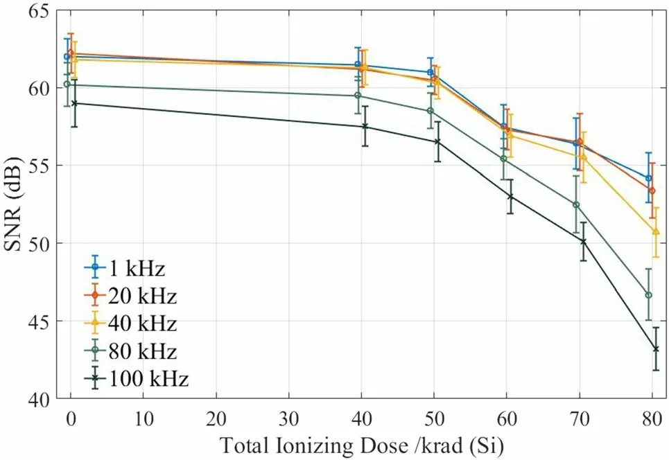
Fig. 7 (Color online) Average SNR variation of formal experiment sample groups with the different input frequencies
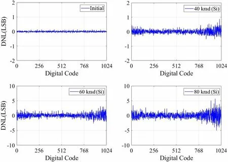
Fig. 5 Differential nonlinear variation of one formal experiment sample after ionizing radiation
where n and t are the number of samples and measurements. For a better display effect, the uncertainty of the total ionizing dose and the electromagnetic field strength is not given in the form of error bars in the figure.
Figure 5 reveals that the DNL of the sample with a TID of 40 krad (Si) degenerated, but most samples showed no digital code with DNL exceeding 1 LSB. However, when the total dose was more than 60 krad (Si), the DNL of all samples increased obviously, especially at a code range from 700 to 1024. When the total dose was as much as 80 krad(Si),the DNL of some samples reached 5 LSB,which means that the convention performance degenerated severely and the output digital data were meaningless.
Figure 6 shows that with the TID increasing, the amplitude of the main frequency peak gradually decreased,while the second harmonic increased. The noise level over the full spectrum had an obvious upward trend. Figure 7 shows the monotonic decreasing trend of the SNR with the TID at all frequency points. When the total dose was less than 50 krad (Si), only a slight decrease of SNR was observed. When the dose reached 70-80 krad (Si), owing to the degradation of the main frequency amplitude and the increase in the harmonic and overall noise level, the SNR was significantly reduced, especially when the main frequency of the input signal was greater than 1/3 the sampling rate.
3.2 Transient experiment
The electromagnetic experiments described in this section and Section 3.3 were conducted with five samples that were not irradiated by ionizing radiation. A transient EMI experiment with the double-exponential pulse was performed within 10 min after the TID test.The field strength of the transient pulse was as much as 20 kV/m, and 200 pulses were delivered to each sample within 10 s at a rate of 20 pulses per second. First, the static input of several voltage levels was applied to facilitate the observation of the output port signal. The transient disturbance of hundreds of millivolts coupled to input and output pins was observed through a high-impedance probe and oscilloscope.However,the digital output of the ADC transmitted to the computer did not show a corresponding data error.For better evaluation of the data error in the entire code range, the average value and maximum value of DNL are defined as Eqs.(2)and(3).They represent the average and the maximum of DNL over the digital code range,respectively.

Fig. 8 (Color online) DNL and SNR with and without single electromagnetic pulse incidence of ADC samples with different TIDs:The SNR was measured with two input signal frequencies

Here, n and i are the number of samples and digital code, respectively. Comparing the Average value and Max value of the DNL and SNR of the data acquired with and without transient electromagnetic pulses, no obvious discrepancy was found for each TID group, as shown in Fig. 8.
The results reveal that the digital output of the ADC under test was almost unaffected by transient electromagnetic pulses. Considering the interference source of the double-exponential pulse with a rising edge of 3.6 ns,most energy was concentrated at the spectrum below tens of megahertz,resulting in a limited coupling efficiency to the IC pins. In this case, the coupled energy of the electromagnetic pulse was not intense enough to activate the protection structure of the IC or to cause permanent damage.The signal input setup and hold time of the ADC were both 50 ns, while the coupled transient interference only lasted less than 20 ns,which is difficult for the sample-hold module to recognize.
3.3 Single-frequency interference experiment
Measurement and simulation demonstrated that the electromagnetic energy at less than 150 MHz was more concentrated inside the ICF target chamber [28]. Obvious peaks at some frequencies existed because of cavity resonance. According to the effects of the conducted EMI,nonlinear distortion caused by an out-of-band interference could be severe [19]. Considering the electromagnetic environment of the ICF chamber and power amplifier parameters, 80-MHz continuous sinusoidal input was chosen as the electromagnetic radiation interference source in this experiment.
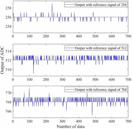
Fig.9 DC response of one ADC sample(before TID irradiation)with different reference signals under the radiated EMI of 2.1 kV/m
The single-frequency interference test was conducted after the samples were irradiated for TID cumulation. For the static input case,the distortion of the output of samples without ionizing radiation at the field strength of 2.1 kV/m is shown in Fig.9.Except for some individual codes,most of the output distortions were not more than 1 bit. However,the distortion appears more serious and denser with a higher reference signal for most samples, with or without ionizing radiation.
To evaluate distortion severity of the ADC output with constant analog input, 10 s of output digital data were collected with a sample rate of 200 ksps for single-frequency interference incidents. The distortion index is defined as the root mean square of voltage deviation, as shown in Eq. (4). The distortion index of a group is the average value of its samples, which is shown in Eq. (5).

Here, m is the number of the output digital data,Vouput,i,nis the corresponding voltage of No. i output digital data of No.n sample,and Vrefis the static reference voltage.In that case,DI and DIgrouprepresent the distortion level of a single ADC sample and the sample group,respectively. Based on the distortion index defined above,the result of output deviation under different TID and field strength of single-frequency is shown in Fig. 10.

Fig. 10 (Color online) Distortion indices with different TIDs and EMI with the reference signals of 256, 512, and 768
The positive trend of the distortion index with the electromagnetic field was obvious and as expected.For the TID, the distortion became more serious with a higher input voltage.A positive correlation between the distortion index and the total dose was also observed. Some nonmonotonic points existed in many groups of samples.
4 Probability threshold analysis
In the study of the reliability evaluation of electronic systems, the failure threshold description of ICs as the basic database is of great importance. Therefore, after examining the phenomena of the DUT under a compound radiation environment, the corresponding failure criterion should be determined according to a specific application scenario for threshold analysis. For precise measurement,the static and dynamic parameters of the ADC used for physical diagnosis equipment are critical.Accordingly,the appearance of missing codes and the degradation of the effective number of bits beyond 1 bit were set as failure criteria in this study. From the perspective of DNL and SNR, the DNL of any digital code beyond 1 LSB and the decrease in SNR beyond 6.02 dB were determined as two main failure modes. The frequency of the input signal for threshold analysis was 100 kHz.
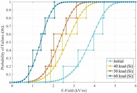
Fig. 11 (Color online) Empirical cumulative distribution function and Weibull distribution fitting curve of ADC with different TIDs,taking DNL beyond 1 LSB as a failure mode
Once the criteria were set,the distribution of the failure threshold could be analyzed.In the reliability evaluation of electronic circuits,the uncertainty comes not only from the measurement error but also from the natural randomness of internal transistor degradation. In general, a test with a large number of samples is preferred if the failure threshold and probability distribution function of the vulnerable circuit are desired. However, the high cost and the limited availability of the devices in question have been a longstanding challenge. Methods for obtaining the failure threshold using small samples have been developed in reliability research for this reason.
The Weibull distribution is one of the commonly used distributions in reliability engineering[27,28].The shapes of the Weibull distribution are flexible with different distribution parameters. This enhances the capability and accuracy of probability distribution fitting with small samples. The probability distribution function and cumulative distribution function of the two-parameter Weibull distribution are

for x>0,β>0,and θ>0.The parameters β and θ are known as the shape and scale parameters,respectively.The failure threshold of the field strength of each TID group was fitted with the Weibull distribution. The groups of 70 and 80 krad (Si) for DNL and 80 krad (Si) for SNR were not included because some samples had already failed just after the TID test. Furthermore, all other groups accepted the relevant hypothesis at the 5% significance level. This means that the Weibull distribution could describe the failure probability distribution of the samples well. The empirical cumulative distribution function and fitting curves of the Weibull distribution according to the two criteria are shown in Figs.11 and 12.The decreasing trend of the threshold is obvious for both failure modes.

Fig. 12 (Color online) Empirical cumulative distribution function and Weibull distribution fitting curve of ADC with different TIDs,taking SNR beyond 6.02 as a failure mode
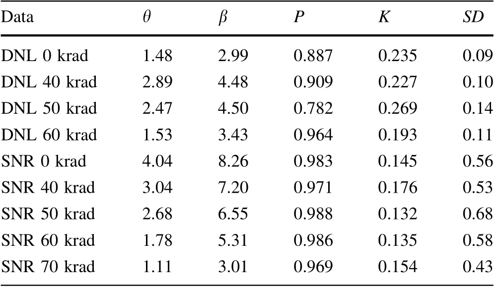
Table 1 Parameters of Weibull and KS test
The fitted parameters were estimated utilizing maximum-likelihood estimation[27].The asymptotic P value P,Kolmogorov-Smirnov (KS) test statistic K, and standard deviation SD of relevant failure mode parameters are given in Table 1. The P value describes the probability that the empirical distribution conforms to the fitted model. From the fitted curves and KS test results, the goodness of fit based on the SNR failure mode appears to be better than that based on the DNL failure mode, as expected. The reason could be that the SNR reflects the overall performance of the transistors inside the DUT. The threshold shifts and leakage current increase of the transistors caused by the TID are the reason for SNR degeneration. In contrast,a more obvious degradation of any comparator inside the ADC may directly result in a large shift to a certain digital code and cause a missing code. As a result, the uncertainty of the DNL failure mode is expected to be greater. Therefore, the SNR or other dynamic parameters that can reflect the overall performance of the DUT are more suitable as a failure criterion for a compound radiation environment.
5 Conclusion
This study focused on the effect on the ADC of both the TID and the electromagnetic radiation environment. The performance degradations under the TID and EMI were observed and analyzed.The DUT showed low sensitivity to electromagnetic pulses. By contrast, the ADC was more vulnerable in the compound radiation environments of ionizing and single-frequency EMI. To investigate the uncertainty of the effects, Weibull distribution fitting with a small sample size was applied, and it described the variation of the threshold well.
However, to evaluate the reliability of an electronic system under a complex radiation environment, more indepth studies are required, especially for high-frequency and high-speed devices. In addition, the annealing after device irradiation increases the uncertainty of test results and puts forward higher requirements for the integration of experimental facilities.
Author contributionsAll authors contributed to the study conception and design. Material preparation, experiment operation and data collection were performed by Ping Wu, Lin Wen and Zhi-Qian Xu.Data analysis was performed by Ping Wu. The first draft of the manuscript was written by Ping Wu, and all authors commented on previous versions of the manuscript. All authors read and approved the final manuscript.
杂志排行

Nuclear Science and Techniques的其它文章
- Design and tests of the prototype a beam monitor of the CSR external target experiment
- Development of a wide-range and fast-response digitizing pulse signal acquisition and processing system for neutron flux monitoring on EAST
- On the viability of wearing evaluation by Thin Layer Activation in the presence of non-occupationally exposed individuals
- Enhancement in optical absorption of CsI(Na)
- Research on tune feedback of the Hefei Light Source II based on machine learning
- Development of a subchannel code for blockage accidents of LMFRs based on the 3D fuel rod model