Enhancement in optical absorption of CsI(Na)
2022-05-12WeiChengPeiShengLiuMinJuYingFengShouZhang
Wei Cheng· Pei-Sheng Liu · Min-Ju Ying · Feng-Shou Zhang,2,3
Abstract Discussions pertaining to enhancement in the luminous efficiency of cesium iodide(CsI)detectors doped with sodium(Na)abound.In this study,the defect structure of one Cs atom replaced by one Na atom is calculated using the ab initio method. Subsequently, the electronic band structures, densities of states, optical absorption spectra,phonons, and transport properties of CsI in perfect and defective structures are investigated. The absorption spectra of CsI with and without Na impurities are compared. It is discovered that the impurity levels in the forbidden band are generated from the shell electron distributions of the impurity atoms,not from lattice distortions.Furthermore,it is discovered that the optical absorption can be enhanced by doping CsI with Na.
Keywords CsI · Na impurity · Band structure · Phonon ·Absorption spectrum
1 Introduction
The research and development of detectors with high luminous efficiency, fast decay time, high mass density,and short radiation length is vital to the promotion of nuclear science and technology [1, 2]. The detection of X-rays, gamma rays, and ion beams requires the use of accurate detectors with a high density and high response speed. Cesium iodide (CsI) is a wide-bandgap inorganic insulator with slight hygroscopy, a relatively high density,a high stopping power, and a high scintillation light yield[3-5]. A perfect CsI crystal emits UV light in the energy range of 3.7 to 4.3 eV when it is excited by external irradiation. The corresponding luminous decay time is approximately 10 ns [6]. CsI has been used in various fields of radiation detection [7].
Free electrons,free holes,and electron-hole pairs can be excited via external irradiation [8]. The perfect CsI crystal is transparent in the visible region, and color centers form easily in CsI under irradiation. It is discovered that defect V1-Cscan introduce visible absorption bands at 2.21 and 3.02 eV [9]. Some de-excitation processes emit photons and provide optical signals. Some de-excitation processes do not emit any photons.These non-radiative de-excitation processes are related to phonons [10]. The number of photons induced by a radiation signal is related to the luminous efficiency. Luminescence is caused by the attenuation of two types of self-capturing excitons[6].The generated photons can be reabsorbed, and the number of output photons is reduced [11]. Reabsorption limits the luminous efficiency. Luminous efficiency is complex and depends on many factors, such as the band structure and electron-phonon interaction. The luminous efficiency is difficult to calculate. It was discovered that the luminous efficiency of pure CsI is low,and that doping is an effective method for improving the efficiency.CsI doped with silver(Ag) and thallium (Tl) yield good scintillators [11, 12].Similarly, CsI doped with sodium (Na) yields a good scintillator with enhanced optical absorption[3, 6, 7, 13-15]. The light yield of CsI doped with Na is extremely high (38,500 photons/MeV) compared with that of CsI (2000 photons/MeV) [13]. As indicated in Ref. [6],the highest emission intensity of CsI doped with Na is nine times higher than that of CsI. From a theoretical perspective, both the photon emission and photon absorption spectra depend on the transition matrix elements between the excited and ground states.These defects can modify the electronic states. Photons are generated by external radiation, whereas some photons are absorbed by the scintillator. Even if the photon emission and photon absorption increase simultaneously, the gain in light yield is significant for CsI doped with Na[6].The luminous efficiency of a good scintillator affords strong absorption in the lowenergy optical spectrum [11].
Defects can be generated during the doping process,some of which are metastable, whereas others are stable [8]. The electronic structures of metastable defects differ from those of fully relaxed defects.This suggests that the defect properties obtained from actual experiments are complex. Doping is a useful technique for obtaining novel properties.One of the disadvantages of doping Na in a CsI scintillator is that the decay time increases during the luminous process. The decay time of one major peak is approximately 430 ns [14]. However, this decay time does not enable fast detection.Using a microscale technique,the decay time decreased significantly to 19 ns [13]. Meanwhile, using a photonic crystal technique, the light output enhanced [1, 15].
The electronic structure and phonon spectrum of CsI doped with Na must be elucidated to understand the mechanism associated with the improvement in luminous efficiency [2, 9, 16]. Ab initio calculations are currently widely used in material research. Many types of ab initio software exist, such as MedeA-VASP [17], Materials Studio [18], Abinit [19], and Quantum Espresso [20], where the methods employed are primarily based on density functional theory (DFT). The macroscopic physical properties can be calculated using suitable microscopic models.The electronic structure, density of states (DOS), optical properties, phonons, and transport properties can be obtained self-consistently. Ab initio calculations for CsI with various defects have been performed. Cedillo and Cortona calculated the bandgaps of CsI at different pressures [16]. Zhao et al. [2] calculated the refractive indices of CsI at different pressures. Ying and Ni calculated the absorption coefficients of CsI with vacancy [9]. Zhang et al. [21]calculated the band structures, DOS, and dielectric functions of CsI doped with Na, Ag, and Tl atoms [11]]. Owing to limited computer resources, the number of atoms in a structure cannot exceed 300 atoms.In most calculations, the defect concentration cannot be less than 1/300 [22, 23].
In this study, undoped and doped CsI materials were modeled with perfect defect structures. It was discovered that impurities can be introduced in the forbidden gap by doping CsI with Na atoms. It is noteworthy that the impurity levels were not caused by lattice distortions. The bandgap decreased with the impurity concentration.Meanwhile, electrons transited easily through the intermediate impurity level within the forbidden gap. The highest-frequency optical branch was associated with Na atoms in the phonon dispersion curve. Both the electrical and thermal conductivities reduced. The enhanced luminous efficiency was due to the impurity level of Na-doped CsI.
2 Theoretical model
The CsI crystal is a simple cubic crystal.The unit cell of CsI in a perfect structure is shown in Fig. 1a. Its space group is Pm-3 m. The defect structures are shown in Fig.1b,c,and d.Three defect structures were created from the unit cell of CsI in Fig. 1a, where each orthogonal direction enlarged by three,four,and five times,separately.The Cs atom at the center of the cell was replaced with a doped Na atom. The abovementioned three defect structures were labeled NaCs26I27, NaCs63I64, and NaCs124I125,respectively.
In this study, calculation was performed based on DFT using the ab initio software MedeA-VASP. The exchange correlation potentials of LDA, GGA-PBE, and the hybrid functional HSE06 were selected [24-29]. In the pseudopotentials, the shell electronic configurations of the Na,Cs, and I atoms were 2p63s1, 5s25p66s1, and 5s25p5,respectively. The total number of valence electrons in the unit cell of the perfect and abovementioned three defect structures were 16, 430, 1022, and 1998,respectively. The cut-off energy was set to 400 eV.The k-meshes were set to 14 × 14 × 14 for the perfect structure and 2 × 2 × 2 for the defect structures.The number of conduction bands was set to 2000 for the defect structures.
The phonon dispersion curves can be calculated using the direct method[30].The perturbed displacements of the atoms were 0.001 nm in the three orthogonal directions.The force constant matrices for each irreducible representation were constructed by considering all possible nontrivial atomic displacements. The interatomic forces were obtained from all calculations. Moreover, the phonon frequencies for each irreducible representation and wavevector k can be obtained.Because GGA overestimates the lattice constant, the phonon frequencies are underestimated. LDA was discovered to be better than GGA for accurately calculating the phonon frequencies. The defect and perfect structures were optimized using the LDA functional in the phonon calculations.Approximate LO/TO splitting was applied to calculate the phonons.

Fig.1 (Color online)Perfect structure of CsI(a).Defect structures of CsI with one Cs atom(light blue ball)replaced with one Na atom(black ball), in which atomic impurity concentrations of Na were 1/54 (b), 1/128 (c), and 1/250 (d)
The electronic and thermal transport properties were calculated using Boltzmann’s transport theory [31]. Fields with chemical potentials within EF± 0.2 eV were considered in the transport calculations. The temperature was set to 300 K.In the defect structure of NaCs63I64,up to 192 electronic bands near the Fermi level were included in the transport calculation.
3 Results and discussion
3.1 Relaxation of defect structures
The total energy of the atoms in the unit cell with different lattice parameters was calculated.The structure with the lowest energy can be selected automatically using the ab initio program. In the program, the minimization of energy includes the optimizations of the lattice parameters and atom locations. The lattice parameter of the perfect structure with the optimized lowest energy was a = 0.467 nm, owing to the cubic lattice symmetry. The calculated lattice parameter was similar to the experimental lattice parameter of a = 0.466 nm for a membrane measuring 500 nm thick [32]. In heavily doped CsI, the lattice parameters must be optimized to represent the actual relaxation. In lightly doped CsI, the defect concentration was low. Most atoms remained in their previous equilibrium positions, and only a few atoms around the doped atom were displaced to new equilibrium positions. To model the defects,it is not necessary to optimize the lattice parameters of the defect structure in most cases. The energy difference with and without a relaxation magnitude of less than 0.02 eV is the optimization criterion.
The lattice parameters of the defect structure in Fig. 1b are a = 1.401 nm without relaxation and a = 1.395 nm after relaxation. The difference between the two lattice parameters was only 0.4%. The relaxation energy in this case was only 0.07 eV. The lattice parameters for the defect structures must be optimized. Based on the optimization criteria,the relaxation of the lattice parameters of the other two defect structures shown in Fig. 1c, d is not necessary.The relaxation energy differences were less than 0.02 eV in these two cases.The effects of external pressure can be calculated by setting different lattice parameters.Zhao et al. [2] discovered that as the pressure increased,both the lattice parameter and band gap decreased. It is noteworthy that ab initio calculations are better than empirical calculations: empirical classical force fields are suitable for only equilibrium lattice parameters with no external pressure, whereas empirical classical force fields fail at high external pressures.
In real materials, internal stresses exist around defects,and the energies of these defect structures are high. The energy decreased during the relaxation process of annealing. In most theoretical calculations, the atom positions in the unit cell are optimized to represent real distortions around the defects. After the relaxation of atoms, it was discovered that the bond lengths of Na-I and Cs-I were 0.3986 and 0.4045 nm, respectively, and that the bond length difference was approximately 1% for the defect structures shown in Fig. 1c. The atomic radius of the Na atom was smaller than that of the Cs atom, and the I atom was closer to the Na atom. This is known as the atomic volume packing effect. Although the local distortion was insignificant, the enhancement in the optical absorption was significant, as will be discussed below.
3.2 Band structure and DOS
The electron dispersion curves of the perfect and defect structures with different Na impurity concentrations are shown in Fig. 2. A total of 16 electrons occupied eight energy levels for the perfect structure,as shown in Fig. 2a.The eight energy levels were categorized into four sets of separate valence bands with energies from low to high,i.e.,the s electrons of Cs atoms, s electrons of I atoms, p electrons of Cs atoms, and p electrons of I atoms. The s electrons were localized around the atoms;therefore,they were delocalized in the reciprocal space. The dispersion curves for the s electrons were flat.The p electrons were similarly localized. No mixing occurred between the s and p electrons in the valence bands.Meanwhile,the bonding of Cs-I was mainly ionic and exhibited an extremely weak covalent characteristic. Both the valence band maximum and conduction band minimum were located at the Γ point.It is noteworthy that CsI is a direct-bandgap insulator.
To investigate the electronic band structures at different defect concentrations, three defect structures were examined, as shown in Fig. 2b, c and d. The atomic impurity concentrations were 1/54, 1/128, and 1/250. Structure NaCs124I125exhibited more bands, as shown in Fig. 2d.The direct bandgap remained in all the defect structures.The dispersion of the valence bands was flat near the Fermi level.The valence and conduction bands became denser as the number of atoms increased. This is due to the band folding of the perfect structure.The small dispersion of the impurity level shown in Fig. 2b was caused by the small unit cell and high defect concentration. Defects typically appeared at the center of the cell,which prevented periodic boundary effects. As the size of the unit cell increased,periodic boundary effects became less important, and the impurity level became flat and dispersionless. The band gaps of the defect structures converged to that of the perfect structure. When the unit cell of a defect structure was enlarged, more computer resources were required. However, the physical conclusions obtained were the same.
A total of 1022 electrons occupied 511 energy levels in the defect structure of NaCs63I64. Most low-energy excitations were related to the valence electrons near the Fermi level. The dispersion curves of the defect structures near the Fermi level are shown in Fig. 2c. One difference between the perfect and defect structures in the dispersion curves is that a new Na level appeared in the forbidden gap.The bandgaps differed for different defect concentrations.The other level in the defect structure was the folding of energy levels in the perfect structure.
The generation of impurities is attributable to two mechanisms. One is the electron distribution of the impurity atom, and the other is the lattice distortion of the host atoms.

Fig. 2 Band structure of CsI in perfect structure a and three defect structures, i.e., NaCs26I27 (b), NaCs63I64 (c), and NaCs124I125 (d).Calculations based on GGA and hybrid functionals of HSE06 are shown in solid and dashed lines, respectively
Cs and Na are alkali elements that contain only one electron in their outermost shells, and their chemical properties are similar. The shell electron distributions of potassium(K)and rubidium(Ru)atoms are similar to those of Cs atoms. The shell electron distributions for all the alkali elements are different. In fact, the pseudopotentials of the core electrons are different.Therefore,the dispersion curves of the defect structures of NaCs63I64,KCs63I64, and RuCs63I64with no lattice distortion must be calculated and then compared with those of the perfect CsI. The comparisons show that an impurity level existed in NaCs63I64,whereas no impurity levels were observed in KCs63I64and RuCs63I64. Based on the calculated dispersion curves, we confirmed that the shell electron distribution of the alkali elements can produce impurity levels in the forbidden bands. A transition occurred when the center of the shell electron approached the nucleus. None of the alkali elements with atomic radii larger than that of Na in CsI can generate impurity levels.
Next, we investigate whether atomic distortion alone can produce impurity levels. We begin with the optimized defect structure of NaCs63I64and then replace Na with Cs.The structure is a distorted CsI without an impurity atom.The dispersion curve of this structure shows no impurity level. Based on the analysis above, we can confirm that atomic distortion alone cannot produce impurity levels.This further verifies that pure CsI is not a good scintillator.Even if some atoms in CsI are distorted by external irradiation,impurity levels are not generated.Improved optical absorption requires impurity levels to be generated by doped Na.
The total DOS of the defect structure NaCs63I64is shown in Fig. 3.The integration of the peaks in the valence bands with the x-axis is equal to the number of electrons in defect structure NaCs63I64. The total DOS in the perfect and undoped structures with 64 Cs and 64 I atoms was almost identical to the defect structure above,based on our calculation. Both Na and Cs are alkali metals with one s valence shell electrons. The partial DOS of the Cs and I atoms in the valence bands were highly localized and not necessarily shown separately,although they are denoted in Fig. 3.The four separate bands with energies ranging from low to high are labeled as Cs-s, I-s, Cs-p, and I-p. The impurity Na level contributed to only one peak at 3.68 eV in the forbidden bands. The integration of the peak in the DOS was only one;therefore,the peak was invisible in the total DOS. The shapes of the total DOS in all the defect structures were similar,and the convergence was excellent.The peak heights were different for the different defect structures because the total number of electrons was different.The shape of the total DOS in the defect structure of NaCs26I27differed slightly from that shown in Fig. 3.Because the Na concentration was extremely high in this case, the peak height of the defect level was evident.
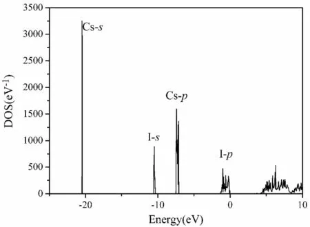
Fig.3 DOS of CsI in defect structure with Na impurity.DOS of CsI in perfect structure is the same,with the same number of atoms.Peak of Na is invisible. Cs-s represents partial DOS for s electrons of Cs atom, etc
A deficiency in DFT underestimates the actual bandgap.The bandgap calculated using the hybrid functional is more similar to the experimental bandgap [26, 27]. Because the bandgaps of all structures were underestimated, the luminescence efficiencies were comparable. The calculated bandgaps are presented in Table 1. Not considering the impurity level, the bandgaps of CsI calculated via DFT in the perfect and defect structures of NaCs127I128were 3.66 and 3.85 eV, respectively, as shown in Table 1. Meanwhile, the impurity level was between 3.57 and 3.75 eV.For a perfect CsI structure, the bandgap calculated using MedeA-VASP (3.66 eV) was similar to that calculated using CASTEP (3.635 eV) [11]. The results calculatedusing the two different software were similar. The experimentally obtained bandgap for CsI was up to 6.2 eV [6].
As the concentration of defects decreased, the defect level became flat in the dispersion curve.At extremely low concentrations, the bandgap of the defect structure approached that of the perfect structure. Using a simple nonlinear fit of the defect concentration and the bandgap listed in Table 1,the defect concentration was estimated to be less than 10-4. The ab initio calculation of thousands of atoms is difficult to realize using computers.
We attempted to improve our bandgap calculation for perfect CsI using the hybrid functional of HSE06. The dispersion curves calculated using the hybrid functional and GGA are shown by dashed and solid lines, respectively, in Fig. 2a.The bandgap calculated using the hybrid functional was 4.53 eV, which is still much smaller than the experimental gap of 6.2 eV.The valence bands near the Fermi level were similar in both calculations. The conduction bands near the Fermi level calculated using the hybrid functional were only a blue shift of those calculated using DFT. This suggests that the ‘‘scissors operator’’ is a good approximation of low-energy optical absorption[33].The bandgap corrected from 3.66 eV (calculated value) to 6.2 eV (experimental value) is a good approximation for investigating low-energy optical absorptions. The I-p valence bands did not indicate any shift.The red shifts of the Cs-s, I-s, and Cs-p valence bands were different. The dispersion curve calculated using the hybrid functional suggests that the ‘‘‘scissors operator’’ will fail if the Cs-s, I-s,and Cs-p valence bands are considered.
3.3 Optical spectrum
The transition between the three separate valence bands below - 7 eV (Cs-s, I-s, and Cs-p) and the doping energy level in the forbidden gap were not considered for lowenergy optical absorption because of the high energy difference.Low-energy optical absorptions were mainly from the highest I-p occupied valence band to the doping level and the lowest unoccupied conduction band. Electronic transitions between valence band I-p and impurity level Na-s were allowed based on symmetry considerations.
Qualitatively, because of the participation of the Na impurity, the transition barrier decreased. However, if symmetry is allowed,then the valence electrons can easily excite to the impurity level, and then from the impurity level to the conduction band. As shown by the absorption spectrum in Fig. 4, an absorption peak appeared at 6.4 eV after the bandgap correction. The absorption peak corresponded to the transition of electrons from the top valence band to the impurity level.

Fig. 4 Absorption spectra of CsI with (dash, dotted, and dash-dotted lines) and without (solid line) Na impurity
We constrained the energy range of the transitions using our program. We set the lowest energies related to the optical transition in the valence bands to - 5, - 10,and - 15 eV.The first case included only the contribution by I-p.The second case included the contributions by both I-p and Cs-p,and the third case included those by I-p,Cs-p,and I-s.Subsequently,we compared the low-energy optical spectra and discovered almost no difference.This suggests that low-energy excitation is only related to the top valence bands, which verifies the conclusion above. We attempted to decrease the number of conduction bands used in the calculations.Consequently,the typical peak height reduced for the defect structures,as shown in Fig. 1c.We conclude that the number of conduction bands involved is important to obtain an accurate optical spectrum for systems with more atoms.
Next, we investigated the optical absorption probability from the defect level to the conduction band.We added one more electron to the defect structure,while maintaining the other parameters. The band structure of the negatively charged system was predicted to be the same as that of the neutral system. The additional electrons remained at the defect level after electronic relaxation.Dipole correction is important to obtain the correct energy for a charged system. After applying the dipole correction, we plotted the band structures and compared them with those shown in Fig. 2. The band structures of the charged systems were almost identical to those of the neutral system. The Fermi level shifted from the valence band maximum to the defect level, which is consistent with the theoretical prediction.
The optical absorption of the negatively charged system was obtained. The extra-strong peak was due to the defect level to the conduction bands. Excluding this strong transition, the optical absorption of the negatively charged structure was similar to that of the neutral structure.
For one defect,as the total number of atoms in the defect structure decreased, the impurity concentration increased,and the optical absorption increased.The defect calculation shows that the transition of electrons from the top valence band to the impurity level was enabled due to symmetry,as predicted theoretically. Consequently, the optical absorption can be increased by doping with more Na atoms,which is consistent with experimental findings[3, 6, 13-15].
To investigate the effect of other defects on light absorption,we calculated the spectra of one iodine vacancy(VI)and one cesium vacancy(VCs).Both spectra show that the optical absorption increased in the low-energy region,which is consistent with the calculations presented in Ref.[9]. The optical absorptions of other atomic doping systems, such as Ag- and Tl-doped CsI, increased as well[9,11].The spectrum of defect VCs-shows two additional absorption peaks at approximately 2.10 and 3.00 eV [9].The dispersion curves of all these doping systems were similar to the dispersion curves calculated in this study.The doping energy levels in the forbidden gap are important for improving the optical absorption efficiency. In addition, the doped Na atoms can induce distortions in the host and reduce the host symmetry. Some previous symmetry-forbidden transitions may have transformed into symmetry-allowed ones. Intrinsic defects exist in pure crystals of CsI; additionally, defect levels exist near the middle of the forbidden bands [6]. These defect levels cause additional absorption in the visible-light range.
3.4 Phonon
CsI is a direct bandgap insulator. The direct bandgap properties are maintained at different doping concentrations. Electron-phonon interactions are important for relaxing radiation-induced excitations, and heat is generated after relaxation. Phonons are important for non-radiative energy dissipation. Therefore, phonon dispersion curves must be examined.In this study,phonon dispersion curves for CsI were calculated using the MedeA software.The macroscopic static dielectric constants were calculated to be 5.60 and 3.68 at the low and high frequency limits,respectively.The Born effective charges were calculated to be 1.32 e and - 1.32 e for the Cs and I atoms, respectively.The phonon dispersion of CsI calculated using LDA is shown in Fig. 5. The phonon dispersion curve agreed well with that shown in Fig. 2 of Ref. [34].The calculated highest frequency of the LO mode was 2.76 THz,which is consistent with the experimentally measured frequency of 11 meV. The vibrational heat capacity at a constant volume was calculated to be 49.6 J/(mol·K) at 300 K.

Fig. 5 Phonon dispersion curve of CsI
The Na impurity in CsI can scatter phonons and reduce the phonon mean free path. Additional phonon collisions can accelerate the relaxation process from the excited state to the ground state. The Born effective charges for defect structure NaCs63I64were calculated. The Born effective charges of the Cs and I atoms were approximately the abovementioned values for pure CsI. The Born effective charge was 1.42 e for the Na atom. The radius of the Na atom was smaller than that of the Cs atom. The attraction between Na+ions and electrons was relatively strong. The macroscopic static dielectric constant was calculated to be 5.72 and 3.71 at the low and high frequency limits,respectively. This suggests that the polarization of CsI can be enhanced via Na impurities. The highest-frequency LO phonons at the Γ point were IR-active T1umodes. The mass of the Cs atom was approximately 5.8 times that of the impurity Na atom, and the frequency of the T1umodes increased to 3.47 THz.
3.5 Transport properties
The electrical and thermal transport properties are related to the lifetimes of the electron and phonon.Electron transitions from higher to lower energy levels emit photons-this is a radiative relaxation process.The probability can be described using Fermi’s golden rule. Moreover,nonradiative processes exist and are related to phonons.We assumed that the sample was not excessively small and disregarded the boundary scattering of the phonons.In this study, we focused on the impurity scattering of phonons.To increase the luminous efficiency, the nonradiative relaxation rate must be reduced. It is preferable to reduce the phonon collision rate and increase the phonon lifetime.Improved thermal transport is associated with longer phonon lifetimes.In general, long mean free paths of phonons enhance the luminous efficiency.The band structures were calculated and are discussed in the sections above. The Fermi surfaces of defect structure NaCs63I64and perfect structure CsI can be constructed using the MedeA software.The calculated electrical conductivity of 0.22 × 10⁵/(Ω·m) for NaCs63I64was less than 1.02 × 10⁵/(Ω·m) for CsI in the perfect structure at 300 K. The calculated thermal conductivity of 0.17 W/(m·K) for the NaCs63I64structure was less than 0.77 W/(m·K)for CsI in the perfect structure. The Seebeck coefficient of both structures was 0.00006 V/K. Impurities can scatter both electron and phonon motions.Impurity scattering is vital to limiting the electrical and phonon mean free paths to reduce both electrical and thermal transport. It was discovered that the thermal-electric performance did not improve, and the nonradiative relaxation did not improve in the transport calculations. This suggests that the impurity-induced perturbation of all the electronic bands near the Fermi level was insignificant.The number of impurity levels was much less than the number of bands near the Fermi level.Additionally, the transport properties were insensitive to the impurity levels, unlike the optical absorption. The increased luminous efficiency was due to the enhanced optical absorption afforded by the impurity levels.
4 Conclusion
In this study,the luminous efficiency of CsI doped with Na was enhanced. The efficiency increased as the Na concentration increased from 0 to 1/54.The impurity levels induced by Na atoms were located in the forbidden band and close to the conduction band. The optical transition between the valence band and intermediate impurity levels was enabled by symmetry. The calculated optical absorption spectra suggest that the enhanced optical absorption is related to the impurity levels.
Acknowledgements The authors thank Professor Xiao-Ping Ouyang for his inputs pertaining to CsI scintillator experiments.
Author contributionsAll authors contributed to the study conception and design. Material preparation, data collection and analysis were performed by Wei Cheng, Pei-Sheng Liu, Min-Ju Ying and Feng-Shou Zhang. The first draft of the manuscript was written by Wei Cheng and all authors commented on previous versions of the manuscript. All authors read and approved the final manuscript.
杂志排行

Nuclear Science and Techniques的其它文章
- Design and tests of the prototype a beam monitor of the CSR external target experiment
- Development of a wide-range and fast-response digitizing pulse signal acquisition and processing system for neutron flux monitoring on EAST
- On the viability of wearing evaluation by Thin Layer Activation in the presence of non-occupationally exposed individuals
- Research on tune feedback of the Hefei Light Source II based on machine learning
- Development of a subchannel code for blockage accidents of LMFRs based on the 3D fuel rod model
- Robust restoration of low-dose cerebral perfusion CT images using NCS-Unet