Frequency dependence on polarization switching measurement in ferroelectric capacitors
2022-02-15ZhaomengGaoShuxianLyuandHangbingLyu
Zhaomeng Gao, Shuxian Lyu, and Hangbing Lyu,†
1Key Laboratory of Microelectronics Device & Integrated Technology, Institute of Microelectronics of Chinese Academy of Sciences,Beijing 100029, China
2University of Chinese Academy of Sciences, Beijing 100049, China
Abstract: Ferroelectric hysteresis loop measurement under high driving frequency generally faces great challenges.Parasitic factors in testing circuits such as leakage current and RC delay could result in abnormal hysteresis loops with erroneous remnant polarization (Pr) and coercive field (Ec).In this study, positive-up-negative-down (PUND) measurement under a wide frequency range was performed on a 10-nm thick Hf0.5Zr0.5O2 ferroelectric film.Detailed analysis on the leakage current and RC delay was conducted as the polarization switching occurs in the FE capacitor.After considering the time lag caused by RC delay, reasonable calibration of current response over the voltage pulse stimulus was employed in the integral of polarization current over time.In such a method, rational P–V loops measured at high frequencies (>1 MHz) was successfully achieved.This work provides a comprehensive understanding on the effect of parasitic factors on the polarization switching behavior of FE films.
Key words: PUND measurement; HfO2-based ferroelectric; RC delay
1.Introduction
Ferroelectric (FE) films have gained significant attention,owing to their potential applications in ferroelectric randomaccess memory (FeRAM)[1], ferroelectric field-effect transistors (FeFETs)[2]negative capacitance field-effect transistors(NCFETs)[3], and neural computation[4].Characterizing the ferroelectricity of FE capacitors with high time resolution is important to investigate the kinetic process of polarization switching in FE films.The hysteresis loop measurement of FE capacitors generally relies on the current response from the voltage pulse stimulus.However, the extraction of the polarization current should be highly influenced by the parasitic factors in a testing circuit, such as leakage current and resistive-capacitive (RC) delay, especially in high driving frequency scope.Up to now, there is still a lack of effective methods to avoid the parasitic factor in hysteresis loop measurement with high driving frequency.Yanget al.investigated the dependence of frequency remnant polarization (Pr= (Pr+–Pr–)/2) and coercive field (Ec= (Ec+–Ec–)/2) in the capacitor with 100 nm Pb(Zr0.2Ti0.8)O3films[5].It was found that as frequency increased from 5 Hz to 2 kHz, almost no change was observed inPr, however, theEcincreased rapidly from 0.2 to 0.4 MV/cm, which was explained by the creep and flow regimes of the FE domain wall motions.However, no explanation was provided for the circularP–Vloop as the frequency further increased.Liet al.observed a similar frequency-dependent trend in the 5 mol% Si-doped HfO2FE thin film, with thePrdecreasing from 20 to 10μC/cm2and theEcincreasing from 0.8 to 1.4 MV/cm as the frequency increases from 1 to 25 kHz[6].The enhancedEcwas explained by the migration of oxygen vacancies from the inner of the HfO2-based FE film to the electrode interface.The properties of the FE films can either be influenced by the inherent factors of FE thin films[7−9], such as different phases (tetragonal, rhombohedral, orthorhombic and momoclinic), defects, grain boundaries and strain (due to misfit and thermal expansion), or by the external test factors[5,10,11], such as the driving frequency, applying voltage,leakage current and RC delay[12−14].In order to investigate the intrinsic mechanism on the ferroelectricity, the parasitic factors in the testing circuit should be well considered and calibrated during measurement.
In this work, the FE hysteresis loops of 10-nm thick Hf0.5Zr0.5O2(HZO) films were measured at different frequencies and voltages by positive-up-negative-down (PUND) methods.The effects of RC delay and leakage current on the hysteresis loops of HZO films were analyzed in detail.After calibrating theP–Vloop with RC delay time at high frequency, the hysteresis loop could be recovered from the circular shape and show reasonableEcandPrvalue.P–Vloop measurement at a high frequency regime over 1 MHz was successfully demonstrated.
2.Experimental details
10-nm thick Hf0.5Zr0.5O2thin films were grown on a NbSr-TiO3(NSTO, 0.1 wt% Nb doping) substrate using tetrakis (dimethylamino) zirconium (TDMAZ) and tetrakis (ethylmethylamino) hafnium (TEMAH) precursors at 250 °C.The 40-nm thick Pt top electrode was deposited by sputtering.Subsequently, rapid thermal processing (RTP) was conducted at 500 °C for 30 s in N ambient.TheI–Vand correspondingP–Vloops were obtained using a probe station equipped with a semiconductor device analyzer (WGFMU, B1500A).The capacitance was measured by a B1520A modular at 100 kHz.
The FE hysteresis loop is generally used to characterize the polarization (P) andEc.ThePis calculated byP=Q/A,whereQis the charge measured by integrating the polarization current over time (t) during a cycle.

The measured current (I) is actually a sum of polarization current (IF), dielectric charge, charging/discharging current(Iε), and the leakage current (IL), i.e.,I=IF+Iε+IL.The leakage current is affected by several factors, including electron tunneling, hopping, and resistive switching caused by polarization reversal.The PUND measurement is an effectively approach to eliminate the contribution of dielectric current and leakage current off from the polarization current[15].It generally contains a set of five voltage pulses.The second (IP) and fourth (IN) measured currents consist of the polarization switching current (IF) and non-polarization switching current (Iε, andIL).The third (IU) and fifth (ID) measured current are comprised of the non-ferroelectricity contributions (IεandIL) only.Thus, the polarization switching currentIFcould be obtained by subtractingIUfromIPandIDfromIN.
3.Results and discussion
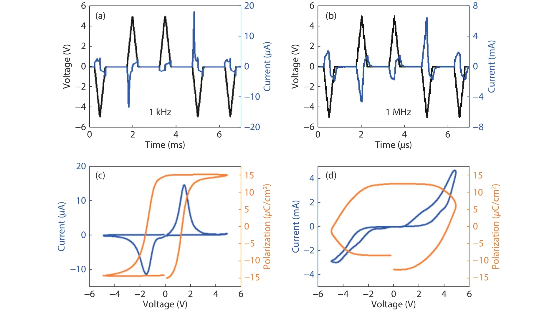
In order to study the influence of frequency on the polarization switching in FE capacitors, we measured the hysteresis loops of the 10-nm thick HZO sample at different frequencies.The device had first undergone a wake-up process with 1000 cycles of 5 V/10 kHz pulses.After that, a ±5 V triangular waveform ranging from 1 MHz to 1 Hz frequencies was applied on the device.Fig.1(a) shows a typical current response of the applied PUND voltage pulse under 1 kHz.The 2nd and 4th relatively higher current peaks clearly show the polarization switching happened in the Pt/HZO/NSTO stack.Fig.1(c) depicts the correspondingP–Vloops calculated from Fig.1(a), with 2Prof ~30μC/cm2and 2Ecof ~2.79 MV/cm.As the frequency increased to 1 MHz, a similar current/voltage response could be observed, as shown in Fig.1(b).However,the current peak exhibits a slight lag behind the voltage peak, indicating a time delay must exist in high frequency case.The correspondingP–Vloop displays a round curve in Fig.1(d), with an increase inEcand decrease inPr.This abnormalP–Vcurve indicates that the time delay must be taken into consideration at high-frequency PUND measurement.

Fig.1.(Color online) Hysteresis loops of 10-nm thick HZO films.(a, b) PUND measurement under 1 kHz and 1 MHz frequency.(c, d) The I–V and P–V loops were obtained from (a, b).The black, blue and orange lines represent applied the voltage, measured current and integrated polarization, respectively.
Detailed results about the influence of voltage and frequency onPrandEcare shown in Fig.2.ThePrandEcwere obtained byP–Vloop measurement with applying voltage from 2 to 5 V triangular waves with frequencies ranging from 1 Hz to 1 MHz.The distributions ofPrandEcwith driving frequency could be divided into regions A, B, and C.When low frequency pulses were applied, corresponding to region A,the device tends to breakdown hard as the voltage amplitude exceeds 3.5 V.This case could be easily understood by a time-dependent dielectric breakdown (TDDB) model[16,17].As the driving frequency further increases (20 Hz–100 kHz, region B), thePrandEcwere monotonically decreased and increased, respectively.The increment ofEcshould be related with voltage drop on the resistance in series (Rs) with HZO film, including the contact resistance of the probe and the electrode, the wire resistance, the NSTO substrate resistance and the instrument resistance.We estimate the in-series resistance by directly measuring the resistance of the Pt/NSTO sample without HZO film (about ~ 500 Ω).As the driving frequency increases, the transient current increases correspondingly, resulting in more voltage divided by the in-series resist-ance.As the frequency enters into region C (>100 kHz), thePrwas found to drop rapidly, accompanied with the much-increasedEc.The measuredP–Vloops were found to be circular, which is quite abnormal considering the leakage current in this case is still low and the HZO film keeps intact without breakdown.Thus, this abnormalP–Vcurve in the high-frequency region should be reasonably resulted from the parasitic factors in the testing circuit.

Fig.2.(Color online) The influence of frequency dependence on ferroelectricity.(a) Pr and (b) Ec were obtained by applying a voltage from 2.0 to 5.0 V under frequency from 1 Hz to 1 MHz for 10-nm thick HZO films.
We first pay attention to the RC delay in the testing circuit, which may affect the integration of the current over time.The RC delay time (τ) could be easily calculated by

whereCis the capacitance of Pt/(10 nm)HZO/NSTO capacitor andRis the resistance in series with HZO film.Under small signalC–Vmeasurement, theCof FE capacitor was found to be about ~67 pF, with the corresponding dielectric constant(ε) of HZO as ~29.8, which has good consistency with the reported value of HZO film[18,19].As mentioned above, theRsin the testing circuit was about ~550 Ω, thus, the RC delay timeτcould be obtained as ~37 ns.Considering the current/voltage response was obtained by forcing voltage in one channel and collecting current in another, it is possible to have a time mismatch between these two channels.Thus, the time lag would actually include two parts of contribution, i.e.,RCdelay in the test circuit and time mismatch of the two force/measure channels.The synchronization accuracy of the testing system was about ~25 ns, and thus, the total time lag of the measured current against applied voltage was about~62 ns.As a result, proper calibration should be needed between the applied voltage force and the current response.
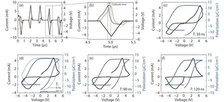
Based on the above analysis, it is necessary to make a proper calibration by moving the current data to the left along the time axis byTns to eliminate the effect of time lag in the PUND measurement, as shown in Figs.3(a) and 3(b).As the calibrate timeTincreases, theP–Vloops changed accordingly, as shown in Figs.3(c)–3(f).WhenTis set to 60 ns (close to the sum ofRCdelay time of 37 ns and data acquisition mismatch of 25 ns), a relatively normal and reasonableP–Vloop could thus be obtained, as shown in Fig.3(e).In the case ofT< 30 ns, insufficient calibration still means the circularP–Vis retained.As theTgets higher than 90 ns, excessive calibration results in the polarization current being over reduced, and therefore rapid decrease ofPrwas observed after calibratingT~ 120 ns, as shown in Fig.3(e).The voltage waveform applied to the capacitor is obtained by cadence spectre simulation usingC= 67 pF,Rs= 500 Ω andRCdelay ~ 33 ns.Similarly, the calibration voltage waveform after moving to the left for 33 ns is consistent with the voltage source waveform,thereby confirming that the calibration method for the shifting of the current is reasonable.A more correct hysteresis loop andEccan be obtained after calibrating the current,which is very important for the study of the dynamics of ferroelectric domains at high frequencies.The good agreement between the calibration time and the actual delay time in the testing circuit also suggests the time lag as the root cause of theP–Vloop during high-frequency measurement.

Fig.3.(Color online) Calibration of P–V loops of Pt/(10 nm)HZO/NSTO capacitor at 1 MHz frequency.(a, b) PUND measurement on a 10 nm HZO film with 1 MHz frequency.The current data (blue line) is moved to the left for time (T) to obtain the calibrated current data (orange line).(c–f)I–V and corresponding P–V loops of 10 nm HZO film after calibrating by different T = 30, 60, 90 and 120 ns, respectively.
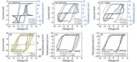
We further applied the time calibration in the PUND measurement with different driving frequencies at 4.5 V, i.e.200 kHz, 500 kHz and 1 MHz, as shown in Figs.4(a)–4(c).Compared with the dotted curves without calibration, theP–Vcurves and correspondingI–Vcurve after calibration exhibit in a much more rational form, indicating high-frequencyP–Vloop measurement above 1 MHz is achievable.TheP–Vloops are obtained in the different areas of capacitors in Fig.4(d).ThePrdecreases andEcincreases as the increase of capacitor area occurs due to the increase in the RC delay as the capacitor area increases.Therefore, a more accurateP–Vcurve can be obtained through proper calibration.Series resistance also affects theP–Vloop by changing the distance between the two probes as shown in Fig.4(e).The calibratedP–Vloops are obtained byT= 10, 30, 40 and 60 ns when the distance between two probes is 0.1, 0.3, 1, 3 and 5 mm.The above results show that the calibration ofRCdelay is necessary at high driving frequency when the capacitance and series resistance are large.These results verify the effectiveness of the calibration method.Future work would be undertaken on the investigation of transient characteristics of FE capacitors.

Fig.4.(Color online) Calibration of P–V loops at different frequencies, capacitor area and series resistance.(a–c) P–V and I–V loops of 10 nm HZO films at 4.5 V under 200 kHz, 500 kHz and 1 MHz initial (dotted line) and after calibration (solid line) T = 60 ns, respectively.(d) P–V loops are obtained in different capacitors area under 1 MHz.The dashed and solid lines indicate ferroelectric current and polarization, respectively.(e, f) P–V loops are obtained at the different distances between two probes under 1 MHz at initial and after calibration, respectively.The connection between the probe and the bottom NSTO electrode is realized by the breakdown capacitor.
4.Conclusion
In this study, we investigated the frequency dependence on theP–Vloop measurement in Pt/(10 nm)HZO/NSTO capacitors by the PUND method.The influence of the parasitic factors on the FE polarization measurement was considered.In the case of the applied voltage with high amplitude and low frequency, large leakage currents could be observed, resulting from the TDDB effect.Further increment of the driving frequency results in reducedPrand increasedEcresult from the voltage drop on the in-series resistance.In the case of high driving frequency, a circular shapeP–Vloop was observed, caused by theRCdelay and data acquisition mismatch of signal channels.After making a proper calibration of hysteresis loop with different series resistance and capacitor areas, a reasonable rationalP–Vloop was obtained at a measuring frequency higher than 1 MHz.This method of current calibration is reasonable, which is proved by cadence spectre simulation of the voltage waveform.This work provides a possible way to investigate the dynamic process of domain switching and ferroelectricity of FE materials at the high-frequency regime.
Acknowledgements
This work was supported by the Ministry of Science and Technology (MOST) of China under Grant 2016YFA0203800,and in part by the National Natural Science Foundation of China under Grants 61834009, 62025406, 92064003,61821091 and the Strategic Priority Research Program of the Chinese Academy of Sciences under Grant XDB44010300.
杂志排行
Journal of Semiconductors的其它文章
- I nvestigation on the passivation, band alignment, gate charge,and mobility degradation of the Ge MOSFET with a GeOx /Al2O3 gate stack by ozone oxidation
- I nvestigation into the InAs/GaAs quantum dot material epitaxially grown on silicon for O band lasers
- High-operating-temperature MWIR photodetector based on a InAs/GaSb superlattice grown by MOCVD
- A 58-dBΩ 20-Gb/s inverter-based cascode transimpedance amplifier for optical communications
- Band gap tuning and p to n-type transition in Mn-doped CuO nanostructured thin films
- Vertical nanowire/nanosheet FETs with a horizontal channel for threshold voltage modulation
