A 58-dBΩ 20-Gb/s inverter-based cascode transimpedance amplifier for optical communications
2022-02-15QuanPanandXiongshiLuo
Quan Pan and Xiongshi Luo
School of Microelectronics and Engineering Research Center of Integrated Circuits for Next-Generation Communications,Ministry of Education, Southern University of Science and Technology, Shenzhen 518055, China
Abstract: This work presents a high-gain broadband inverter-based cascode transimpedance amplifier fabricated in a 65-nm CMOS process.Multiple bandwidth enhancement techniques, including input bonding wire, input series on-chip inductive peaking and negative capacitance compensation, are adopted to overcome the large off-chip photodiode capacitive loading and the miller capacitance of the input device, achieving an overall bandwidth enhancement ratio of 8.5.The electrical measurement shows TIA achieves 58 dBΩ up to 12.7 GHz with a 180-fF off-chip photodetector.The optical measurement demonstrates a clear open eye of 20 Gb/s.The TIA dissipates 4 mW from a 1.2-V supply voltage.
Key words: bandwidth enhancement; CMOS optical receiver; cascode; inductive peaking; negative capacitance; transimpedance amplifier (TIA)
1.Introduction
With the continually growing demand of multimedia applications and cloud computing, the promotion of highspeed communication is becoming more and more urgent.However, conventional copper-based links are no longer adequate for high-speed communications.Compared with copper-based links, the optical interconnection is a more costeffective and reasonable solution due to its excellent stability,high-power efficiency, low-cost and broadband superiorities.A typical optical communication receiver mainly includes a transimpedance amplifier (TIA), limiting amplifier (LA), clock and data recovery (CDR) and de-multiplexer (DMUX)[1].Among them, the TIA is the most critical block as it plays a crucial role in determining the noise, sensitivity and bandwidth performance of the whole receiver system.Various circuits designs, based on a common gate (CG)[2], regulated cascode(RGC)[1,3,4]and shunt resistive feedback[5,6]configurations,have been presented to enlarge the TIA bandwidth.The biggest challenge of the TIA design comes from the large parasitic capacitance of the photodetector (PD), which limits both bandwidth and noise performance.CG or RGC TIA is an effective way to lower the input resistance, thus enhancing the bandwidth performance, however, it tends to consume more power and introduce more noise due to the existence of the active feedback stage.Inverter-based TIA with resistive feedback seems to be a reasonable scheme as it achieves a sufficient bandwidth without large power consumption[7].However, the required high voltage gain of the core amplifier will lead to excessive input capacitance including the gate capacitanceCggand Miller capacitanceCgd, and, in contrast,small voltage gain will lead to too large equivalent input resistance[8, 9].
This work proposes an inductive-peaking inverter-based cascode TIA, which not only obtains high voltage gain of the core amplifier, but also effectively reduces the Miller effect fromCgd.In addition, this TIA utilizes the cascode topology in its core amplifier, achieving better noise performance than its conventional inverter-based alternative.Series inductive peaking and negative capacitance techniques are also employed to further boost the bandwidth.
2.Circuit design
2.1.TIA design
Fig.1 shows the block diagram of the proposed TIA.A pseudo-differential structure is adopted to simultaneously achieve both the input current-to-voltage signal conversion and single-ended to differential signal conversion.The offchip PD conducts input optical to electrical signal conversion.The PD contributes the most capacitance at the input node,i.e., 180-fF capacitive loading in this design.The bonding wire with a reasonable inductanceLBWconnects the off-chip PD and the TIA.The core amplifier incorporating with the shunt feedback resistorsRFmagnifies the input current signal to the voltage signal with a transimpedance gainZTIA.The negative impedance convertor (NIC) technique is adopted to generate a negative capacitance to neutralize the large capacitance at the output node.Finally, a classical open-drain output buffer drives the off-chip 50-Ω load, in which additional NIC is naturalized again for the purposes of a higher bandwidth, higher area efficiency and DC level alteration.It is worth mentioning here that the parasitic capacitors in the NIC are already sufficient for bandwidth compensation in the buffer design.
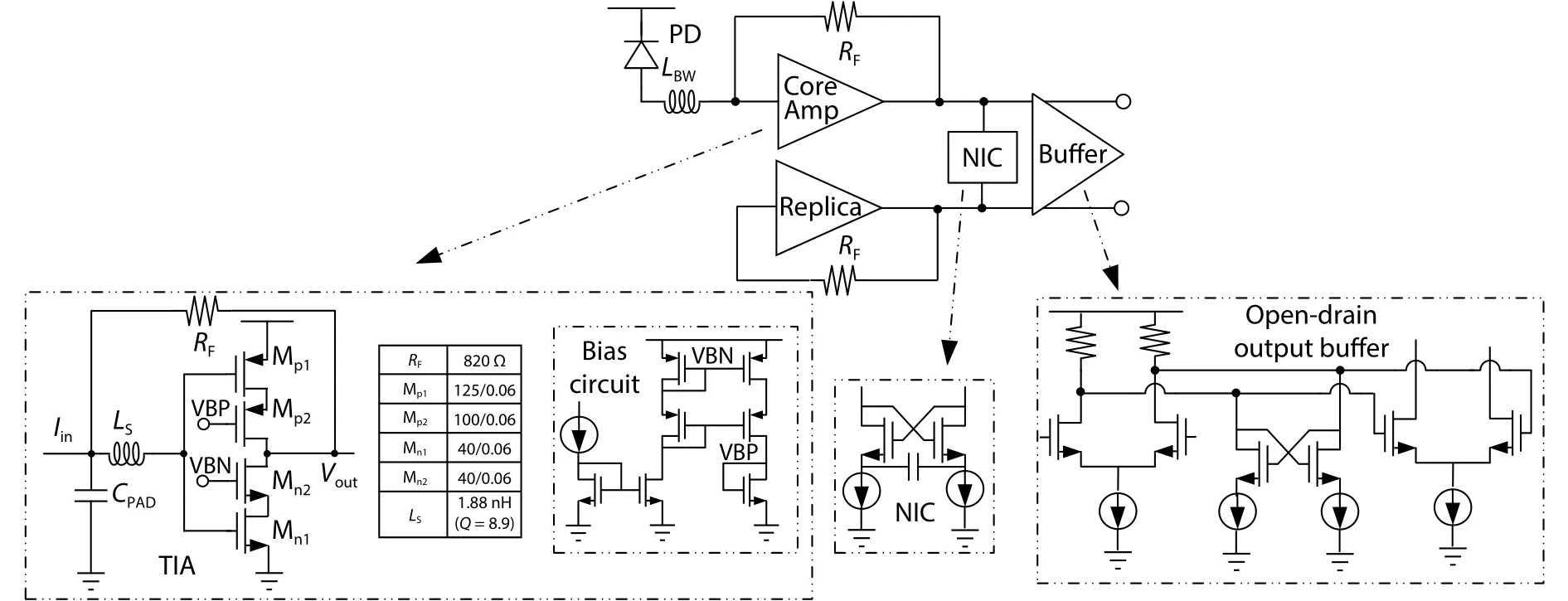
Fig.1.Schematic of the proposed TIA.
The low-frequency transimpedance gain of a shunt resistive TIA is determined by the shunt resistorRF, as the lowfrequency transimpedance gain is given by[7]

A common-source (CS) amplifier and inverter-based amplifier are two common choices for the TIA’s core amplifier.However, on one hand, the CS amplifier is difficult to provide sufficient voltage gain; on the other hand, the inverter-based amplifier can provide adequate voltage gain but introduce large capacitanceCinat the input node and also large Miller capacitance.In this work, an inverter-based cascode amplifier,which provides high open-loop gain and suppresses Miller effect, is adopted as the core amplifier to overcome these issues, as shown in Fig.2.A bias circuit is applied to generate the gate voltage ofMp2andMn2, and both the input and output signal swing of the TIA is small enough to allow them to operate in the saturated region.Table 1 provides input capacitance comparison between inverter-based and inverter-based cascode configurations.As shown, the inverter-based cascode amplifier can not only obtain sufficient gain, but also introduce much less capacitance at the input node.

Fig.2.(Color online) Single-stage shunt resistive feedback TIA in (a) original inverter-based configuration, (b) proposed inverter-based cascode configuration, and (c) the comparison of voltage gain between inverter-based amplifier and inverter-based cascode amplifier.

Table 1.Comparison of inverter-based and inverter-based cascode amplifier.
2.2.Bandwidth enhancement technology
In the optical receiver design, series inductive peaking is a common bandwidth extension method.Placing an inductor between two shunt–shunt capacitors, a better bandwidth is obtained by capacitive splitting.Two inductorsLBWand on-chipLSare used to form two π-networks (Fig.3) to isolate the large PD capacitanceCPD, the PAD capacitanceCPAD, and the input stage’s capacitanceCin.LBWandLSneed to be tuned carefully, otherwise too large inductance in the π-networks would lead to an undesirable ripple in the TIA’s gain response[10], introducing large delay variation and causing the output eye-diagram closure.

Fig.3.Small-signal model of the proposed TIA.
The schematic of input series peaking network and small signal model of the main TIA is shown in Fig.3.The total transimpedance gainZTIAcan be expressed by

whereHs,in(s) is the transfer functionIin/IPDin the input series peaking network andZTIA,main(s) is the transimpedance gain of the main TIA.The transfer functionHs,in(s) can be written as

whereZinis the equivalent input impedance of the main TIA,andZincan be derived as

AndZTIA,maincan be derived as

As shown in the Fig.3(b), the on-chip inductorLSis inserted to form the second π-network which isolatesCPADfromCinand generates the second frequency peaking.With the absence ofLS, the currentIinflowing from the previous input network will be diverted intoRinandCPAD+Cin.Therefore,the output voltage of the latter network is limited by the time constantRin(CPAD+Cin).By inserting theLSto isolateCPADfromCin, the currentIincan charge theCPADfirst.Hence, the input network bandwidth is enhanced.
Fig.4(a) shows the procedure to find the optimal value ofLBWin the first π-network.In this TIA design,Zinis set to be 80 Ω after making a trade-off between bandwidth and gain.LBWis set to be 0.9 nH as the BWER (the bandwidth ratio after/before adopting bandwidth enhancement techniques)changes little for ±20%Zin.In reality, it is difficult to control the bonding wire accurately[7].Therefore, in this design,LBWis designed to have a tolerance of ±25%, hence the targetedLBWis 0.72–1.08 nH.In this range ofLBW,Hs,in(s) shows a small variation of bandwidth and less than a 1-dB gain ripple (Fig.4(b)).The optimization ofLSis also conducted with the consideration of BWER as shown in Fig.4(c), a 1.88-nH on-chip spiral inductor with a quality factor of 8.9 is selected to achieve the optimal BWER.
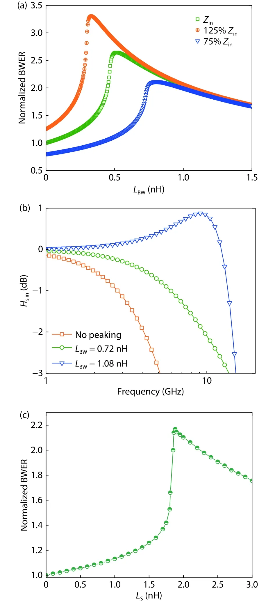
Fig.4.(Color online) (a) BWER of Hs,in(s) in ±25%Zin.(b) Frequency response of the input series peaking network in target LBW, and (c)BWER of ZTIA(s) varies with LS.
Although, inverter-based cascode TIA can provide smaller input capacitance, the bandwidth at the TIA open loop output node is limited by large output impedance introduced by cascode configuration.In order to reduce the sensitivity of TIA output node to capacitance, the negative impedance convertor (NIC) technique[11]is adopted in the TIA output node to generate a negative capacitance to neutralize the capacitance at the TIA output node (Fig.5).According to the half-circuit analysis in Ref.[11], the equivalent input impedance can be expressed by
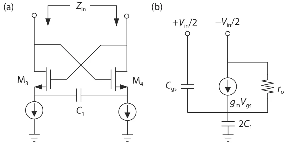
Fig.5.(a) Schematic of negative impedance converter.(b) Half-circuit analysis of cross-couple topology.

WhenC1is large enough, Eq.(9) could be simplified as

The derivation result shows that the negative impedance generates a negative impedance and negative capacitance, which can be used to neutralize the capacitive loading and boost the bandwidth in the output network.The crosscoupled NIC cooperated with the load may become relaxation oscillators[12].To avoid potential oscillation due to the NIC, its loop gain is carefully designed to be far away from 0 dB.The frequency response of TIA when applying the multiple bandwidth extension schemes is shown in Fig.6.Compared with the conventional inverter-based configuration,when the inverter-based cascode configuration is employed,the TIA bandwidth is increased from 1.5 to 6 GHz.With the inductance peaking technique, the bandwidth is broadened to 11.5 GHz, and with the NIC technique, the bandwidth is broadened to a maximum of 12.7 GHz.Overall, these bandwidth enhancement techniques achieve a bandwidth enhancement ratio of 8.5.
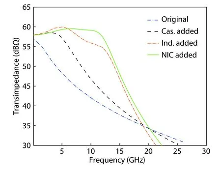
Fig.6.(Color online) Post-layout simulation of progressive TIA bandwidth enhancement.
2.3.Noise analysis
The noise mainly generates from the feedback resistor and the core amplifier of TIA.Using the method in Ref.[9],the total input referred noise (IRN) can be written as

whereCtotis the sum ofCPD,CPADandCin, and theis the input-referred noise of the core amplifier.As the cascode amplifier provides a larger open loop gain, the feedback resistor is allowed to be larger when achieving the same bandwidth.Meanwhile, a large feedback resistor can effectively reduce the IRN of an optical receiver system.SmallerCtotalso further improves IRN.Compared with the inverter-based TIA,noise contributions from Mp2andMn2to the output node in the inverter-based cascode topology is negligible, especially at low frequency because of largeron1androp1[11].Nevertheless, if the parasitic capacitanceCdsof Mn1and Mp1is considered, the noise generated by Mn2and Mp2will contribute to the output node at high frequency.However, due to the increase of bandwidth, IRN can maintain a relatively low value over a large frequency range.Table 1 shows the calculatedof both topologies and Fig.7 shows the post-layout TIA noise simulation, in which the results are consistent with the above analysis.The analysis above testifies the proposed TIA will obtain greater bandwidth gain product theoretically and maintain a relatively low IRN contribution simultaneously.In addition, in order to minimize the noise contributing from NIC, thegmof NIC is well limited, therefore, the noise of NIC does not have a significant impact on the total IRN current, which is negligible.Therefore, since it could achieve a higher transimpedance gain, the total integrated IRN over the TIA bandwidth concerned is smaller than its inverter-based alternative.Fig.7 indicates that the calculated IRN achieves 4.5which is very competitive compared to recent work.
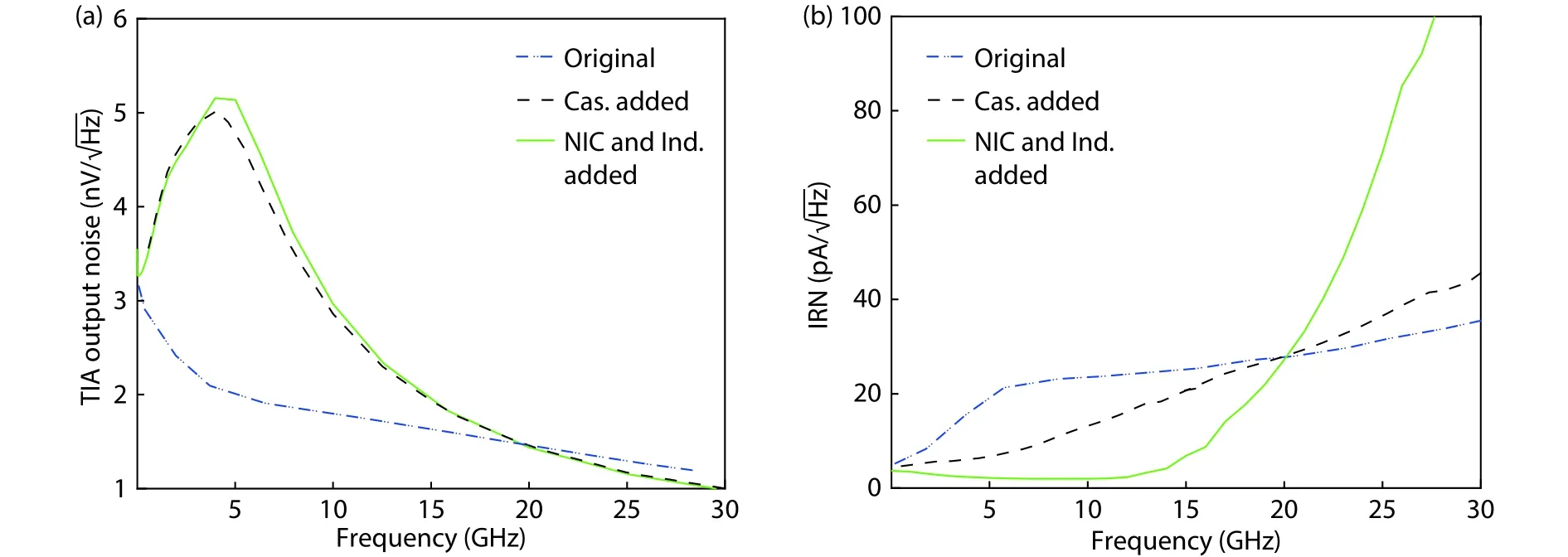
Fig.7.(Color online) Post-layout simulation of (a) TIA output noise and (b) IRN current.
3.Experimental results
The proposed TIA circuit is implemented in TSMC 65-nm CMOS process with an area of 0.25 × 0.13 mm2as shown in Fig.8(a).Fig.8(b) depicts measurement setups for both electrical frequency response and optical eye-diagram test.The probing of the chip-on-board (CoB) captures theS-parameters, which can be converted to the TIA’s transimpedance by

Fig.8.(Color online) (a) Chip micrograph and (b) measurement setup.

whereZ0is 50 Ω.Fig.9 shows that this design achieves a measured transimpedance gain of 58 dBΩ and a –3-dB bandwidth of 12.7 GHz.As shown in Fig.8(b), driven by nonreturn-to-zero (NRZ) pseudo-random binary sequence (PRBS)generator (with 215–1 bit rate), the 30-Gb/s 850-nm Photline Mach–Zehnder Modulator provides a NRZ 215–1 optical input.The modulated optical transmitter then injects the optical signal onto the wire-bonded off-chip PD (0.5-A/W GaAs) via one multiple-mode fiber (MMF).The 20-Gb/s eye-diagram is then measured using a high-speed sampling oscilloscope 86100D.As shown in Fig.10, with PRBS-15 input, the rms and p-p jit-ter of measured TIA output eye diagram are 3.04 and 13.46 ps, respectively, and the signal–noise ratio (SNR) is 7.59.

Fig.9.(Color online) Measured transimpedance gain.

Fig.10.(Color online) Measured PRBS-15 optical eye diagram at 20 Gb/s.
The comparison of this work with recent published work is summarized in Table 2.Due to its pseudo-differential characteristics, this TIA wastes 4-mW power in its dummy block, but it achieves differential outputs.This work achieves the stateof-the-art GBW.

Table 2.TIA performance comparison and summary.
4.Conclusion
This paper presents a pseudo-differential multiple inductive-peaking inverter-based cascode TIA fabricated in TSMC 65-nm CMOS process with an active area of 0.0325 mm2.The bandwidth optimization scheme is elaborated in detail.The measurement results show that this TIA can achieve a gain of 58 dBΩ up to 12.7-GHz bandwidth and 20-Gb/s clear data rate.
Acknowledgements
This work was supported in part by the National Natural Science Foundation of China under Grant 62074074, in part by Natural Science Foundation of Guangdong Province under Grant 2021A1515011266, and in part by the Science and Technology Plan of Shenzhen under Grants JCYJ20190809142017428 and JCYJ20200109141225025.
杂志排行
Journal of Semiconductors的其它文章
- I nvestigation on the passivation, band alignment, gate charge,and mobility degradation of the Ge MOSFET with a GeOx /Al2O3 gate stack by ozone oxidation
- I nvestigation into the InAs/GaAs quantum dot material epitaxially grown on silicon for O band lasers
- High-operating-temperature MWIR photodetector based on a InAs/GaSb superlattice grown by MOCVD
- Band gap tuning and p to n-type transition in Mn-doped CuO nanostructured thin films
- Vertical nanowire/nanosheet FETs with a horizontal channel for threshold voltage modulation
- Frequency dependence on polarization switching measurement in ferroelectric capacitors
