Growth of high quality InSb thin films on GaAs substrates by molecular beam epitaxy method with AlInSb/GaSb as compound buffer layers∗
2021-03-11YongLi李勇XiaoMingLi李晓明RuiTingHao郝瑞亭JieGuo郭杰YuZhuang庄玉SuNingCui崔素宁GuoShuaiWei魏国帅XiaoLeMa马晓乐GuoWeiWang王国伟YingQiangXu徐应强ZhiChuanNiu牛智川andYaoWang王耀
Yong Li(李勇), Xiao-Ming Li(李晓明), Rui-Ting Hao(郝瑞亭),†, Jie Guo(郭杰),Yu Zhuang(庄玉), Su-Ning Cui(崔素宁), Guo-Shuai Wei(魏国帅),Xiao-Le Ma(马晓乐), Guo-Wei Wang(王国伟),‡, Ying-Qiang Xu(徐应强),Zhi-Chuan Niu(牛智川), and Yao Wang(王耀)
1School of Energy and Environment Science,Key Laboratory of Renewable Energy Advanced Materials and Manufacturing Technology of the Ministry of Education,Yunnan Normal University,Kunming 650092,China
2Key Laboratory for SLs and Microstructures,Institute of Semiconductors,Chinese Academy of Sciences,Beijing 100083,China
3Synergetic Innovation Center of Quantum Information and Quantum Physics,University of Science and Technology of China,Hefei 230026,China
4National Center for International Research on Green Optoelectronics,Guangdong Provincial Key Laboratory of Optical Information Materials and Technology,Institute of Electronic Paper Displays,South China Academy of Advanced Optoelectronics,South China Normal University,Guangzhou 510006,China
Keywords: compound buffers,AlInSb/GaSb,defect inhibition,InSb,molecular beam epitaxy(MBE)
1. Introduction
In the III–V group material system, InSb has attracted wide attention due to its high electron mobility,narrow direct band gap, and low effective mass.[1–6]After years of development, it has become an important material for the fabrication of 3µm–5µm infrared detector.[7,8]At present,there are many ways to growth InSb materials, and the InSb epitaxial thin films fabrication by MBE has become one of the preferred methods due to the advantages of high uniformity,in-situ doping,real-time control,and no need of thinning.[9,10]The selection of GaAs substrate materials with semi-insulating and high resistance provides convenient conditions for the fabrication of InSb optoelectronic devices,and also makes InSb materials in infrared focal plane array detectors easier to mix with siliconbased charge couplers for interconnection.[11,12]However,the main challenges in the epitaxial growth of InSb on GaAs substrate is that the lattice mismatch of 14.6% between the two materials will lead to large surface roughness and high dislocation density,and the structure and electrical properties of the epitaxial materials will be affected in varying degrees.[13]According to the literatures,high-quality InSb thin films are usually fabrication by two-step growth,and high-quality materials are also obtained by using other buffer layers structure.[14–16]In addition,in recent years,attention has been paid to adding AlInSb to InSb materials to improve the overall electrical performance of InSb. For example, AlInSb is added to InSb as a barrier layer to reduce the dark current and improve the operating temperature of the device.[17–20]Therefore, AlInSb is used as a buffer layer to suppress the defects caused by lattice mismatch and provide a reference for the integration of AlInSb/InSb materials.
In this paper, high-quality GaSb layer is grown by MBE method on GaAs substrate, and then the epitaxial AlInSb buffer layer with similar InSb lattice. The compound buffer layer is designed to release the strain caused by lattice mismatch between substrate and epitaxial layer, and explore the effect of AlInSb interface layer structure on defect density. At last,InSb thin films were grown onto compound buffer layers,the obtained structures were also studied.
2. Experimental details
The equipment used in this experiment is GEN-II molecular beam epitaxy system produced by Veeco,and using GaAs SI as substrate. The substrate was pre degassed at 200◦C and 400◦C respectively to remove residual water molecules before growth,and then degassed at 800◦C for 15 min in the growth chamber to remove the oxide on the substrate surface. After that, the temperature was reduced to 700◦C and the 300-nm GaAs buffer layer was deposited to cover the residual oxide to flatten the substrate surface. Then, 600-nm GaSb buffer layer was deposited at Tc(GaSb surface reconstruction conversion temperature) +60◦C and 0.25-ML/s condition, and 2 µm AlInSb buffer layer with different interface structures was deposited onto the GaSb layer as the compound buffer layer afterwards:
(B1): Gradient layer buffer Al0.35In0.65Sb(500 nm)/Al0.25In0.75Sb (1.5 µm) with high Al component interlayer.
(B2): A three-period superlattice interlayer buffer of [Al0.35In0.65Sb (83 nm)/Al0.15In0.85Sb (83 nm)]×3/Al0.25In0.75Sb(1.5µm).
Finally,3-µm InSb thin films were further grown onto the buffer layer structure of samples B1and B2at Tcbeing 5◦C and 0.6-ML/s condition, and denoted as samples C1and C2.Meanwhile,InSb thin film sample C3without buffer layer was also grown as the reference group. The evolution process of surface morphology was observed. The detailed structure of samples is illustrated in Fig.1. In the whole epitaxial process,the growth parameters we adopted were optimized according to Ref. [21] in order to ensure the material quality. The parameters include growth rate, substrate temperature (material growth temperature),and III–V beam flux ratio.
The surface morphology and defects of samples were studied by using Digital S-II nano Navi atomic force microscope (AFM) and optical microscope. The crystal quality was identified by high resolution x-ray diffraction(HRXRD).RHEED is used for in-situ monitoring the growth process and calibrating the reconstruction conversion temperature Tcof GaSb surface(Fig.2).

Fig.1. Schematic representation of heterostructure growth of the InSb thin films structure with various structures of each layer.
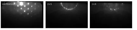
Fig.2. RHEED diagram of GaSb epilayer surface with nucleation stage and reconstruction conversion occurred(from 2×5 to 1×3).
3. Results and discussion
Figure 3 shows the AFM morphology of the GaSb buffer layer on GaAs substrate, and the surface presents a typical pyramid-like structure, which has been reported in the previous investigate.[22,23]The scale of pyramid-like structures in the 10µm×10µm range has continuous changes. Careful observation on the junction of the adjacent great pyramid-like structures (in Fig.3 (10 µm×10 µm)) was conducted to reveal the feature of the small pyramid-like structures outcrops,which are the results of spiral growth and accumulation of atoms around threading dislocations. In the range of 2 µm×2 µm, the pyramid-like structures on the surface of GaSb epitaxial layer presents a terrace-like sidewall with atomic steps, and there are interrupted atomic steps at the side wall,which is also a feature of threading dislocations outcrops. At the same time,large strain is exiting at the intersection of the adjacent pyramid-like sidewalls. When 2-µm AlInSb buffer layer was grown on GaSb surface, the pyramid-like structure was replaced by a flat surface with atomic step stripes, indicating that AlInSb buffer layer interrupted the propagation of most threading dislocations. However,different AlInSb buffer layers still show different effects on defect suppression.
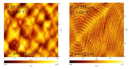
Fig.3. AFM surface morphologies of the GaSb buffer grown on GaAs substrates with different scanning ranges.
The AFM images in Fig.4 shows the comparison of morphologies characteristics of the AlInSb/GaSb compound buffer layer with different interface structures. The results shows that the size and density of edge dislocation are related to the structure of AlInSb interface layer.AFM images of sample B1revealed that the edge dislocations on its surface terminate the continuity of atomic arrangement. The edge dislocation may be caused by the sliding and extending of the stacking fault under the extrusion of the pyramid-like sidewalls on the GaSb surface, and vertically across the AlInSb interface to the epitaxial layer surface. At the same time, due to some threading dislocations crossing the interface layer, atoms spiral grown around it form a hillock,which is a typical form of defects caused by lattice mismatch. Compared with sample B1, sample B2presents a smoother surface with lower defect density, small average height and diameter. The results show that the superlattice buffer layer can effectively release the internal strain of epitaxial materials and reduce the structural defects.
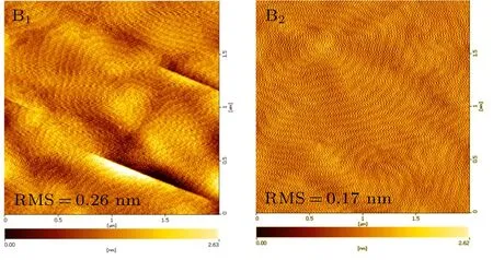
Fig.4. AFM surface morphology of AlInSb compound buffer layer(2µm×2 µm) with (B1) high Al content AlInSb as interface layer, (B2) AlInSb superlattice as interface layer.
In order to determine the strain relaxation mechanism of buffer layer and the residual strain in epitaxial layer,TEM tests were carried out to study the interface of samples B1and B2.The types and distribution of dislocations in the buffer layer were well characterized. Due to the small difference in the composition of AlInSb interface layer,the delamination structure of AlInSb interface was not observed in TEM images,but the effect of interface layer can be evaluated according to defect distribution. As shown in Fig.5,there are a large number of dislocations in sample B1. A series of complex dislocation types cross the interface layer and extend to the epitaxial layer. Among them,most of the 60◦dislocations form closed dislocation loops in the buffer layer and annihilate each other.Therefore,the 90◦edge dislocation is dominant,and some of them are generated at the top of epitaxial layer.This is also the main source of edge dislocation in Fig.4. It is demonstrated that the relaxation process in the initial 500-nm interface layer of AlInSb has not completed, and the epitaxial material still has large strain and produces new edge dislocations. Compared with sample B1, sample B2presents different strain relaxation mechanisms,and the defects are mainly concentrated in the initial 500-nm interface layer, and low density dislocations were observed at the top of AlInSb buffer layer, which indicated that the continuous SL structure with elastic strain interrupted the propagation of dislocations,a large number of dislocations were annihilated in the growth process, and the rapid relaxation of AlInSb buffer layer was achieved. The results of TEM show that the introduction of superlattice structure is beneficial to the overall function of the buffer layer design.
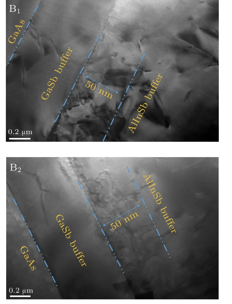
Fig.5.TEM spectrum of AlInSb compound buffer layer(2µm×2µm)with(B1)high Al content AlInSb as interface layer, (B2)AlInSb superlattice as interface layer.
Based on the optimized results of buffer layer,3-µm InSb thin films were further grown onto the buffer layer structures of samples B1and B2respectively. The evolution process of surface morphology was observed.
Figure 6 shows the AFM surface morphology of InSb thin films sample. Sample C1adopts the buffer layer structure of sample B2. At the same time, it also inherits the generation mode of edge dislocation in sample B2, and intensifies the size of edge dislocation. Its surface is filled with a large number of edge dislocation and uneven mound with obvious layered step structure. The surface roughness(RMS)is 0.57 nm(2 µm×2 µm). For the sample C2with superlattice buffer layer, its presented a smoother surface morphology without obvious mound and edge dislocation characteristics, indicating that a large number of defects were suppressed while the processes of buffer layer growth, and the surface roughness(RMS) is as low as 0.18 nm (2 µm×2 µm). Compared with the surface of InSb thin film directly epitaxial on GaAs substrate (sample C3), we can find that the addition of buffer layer greatly improves the epitaxial quality of InSb thin film.When InSb sample is directly epitaxed on GaAs substrates, a large number of edge dislocations are found on the surface of InSb sample, and the surface roughness (RMS) is as high as 1.30 nm(2µm×2µm). It is indicated that the large mismatch InSb functional layer is not completely relaxed,which results in the deformation of epitaxial layer under the strain. This kind of defect destroyed the continuity of the material structure, and also formed a high-speed channel for electrons and holes,which seriously restricts the performance of the device.The surface distinction of three groups of samples shows the importance of buffer layer for heteroepitaxial growth,and also shows the influence of the difference of buffer layer structures design on material growth.
Similar to the evolution of AFM surface morphology,the optical microscope results of samples also show the defect change(Fig.7). Samples C1and C2have similar mound-like surface morphology,but sample C1has higher mound density under the same observation multiple. However, the surface state of sample C3is completely different,and there are more fracture-lines under the action of strain,which is also the main feature of the edge dislocation in AFM.
Gathering the results of AFM, HRXRD diffraction(Fig.8)carried out for the three groups of samples,the similar conclusions were obtained. The results of HRXRD diffraction patterns could reflect the difference of material quality.InSb sample C2with superlattice buffer has the optimum crystal quality,and the FWHM of InSb diffraction peak is 248 arcsec.For sample C1with high Al-content interface buffer layer,the crystallization quality is slightly worse than that of sample C2,and the FWHM of InSb diffraction peak is 392 arcsec.The C3samples without buffer layer show the worst crystallization quality. The InSb diffraction peak in HRXRD diffraction pattern shows a wide bulge,and the FWHM is up to 525 arcsec.
In order to further determine the quality of InSb thin films,four probe electrical Hall tests were carried out on three groups of samples (C1, C2, C3) with different buffer structures. The results are shown in Table 1. Compared with Table 1 (C2) and other samples, it can be seen that sample C2with superlattice buffer layer has the highest electron mobility of 5.91×104cm2/V·s at room temperature (300 K), and ptype transition occurs at low temperature(77 K).The electrical properties of sample C1are slightly lower than that of sample C2, but the electron mobility decreases abnormally from 300 K (5.14×104cm2/V·s) to 77 K (5.00×102cm2/V·s),which has been reported in many literatures.[24]The electron mobility of C3is the lowest one at room temperature(300 K),the value is 1.17×104cm2/V·s, and the test results are abnormal at 77 K. Hall test results show that the introduction of superlattice buffer layer can improve the overall electrical properties of InSb thin films.
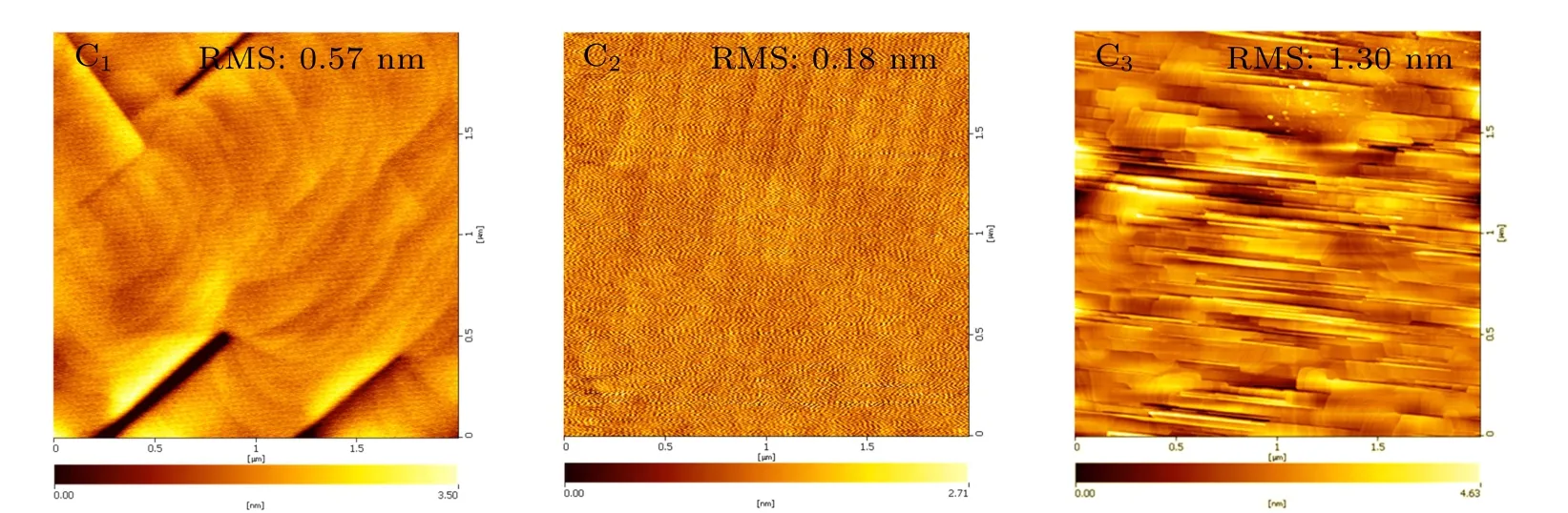
Fig.6. AFM surface morphology of InSb thin film sample (2 µm×2 µm) with (C1) high Al content AlInSb as interface layer, (C2) AlInSb superlattice as interface layer,(C3)directly epitaxial InSb thin films on GaAs substrates.
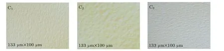
Fig.7. Optical microscope spectrum of InSb thin film sample (133 µm×100 µm) with (C1) high Al content AlInSb as interface layer, (C2)AlInSb superlattice as interface layer,(C3)directly epitaxial InSb thin films on GaAs substrates.
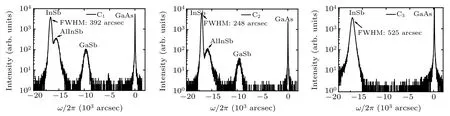
Fig.8. High-resolution x-ray diffraction of InSb thin films specimens with(C1)high Al component AlInSb as interface layer,(C2)AlInSb superlattice as interface buffer layer,(C3)directly epitaxial InSb thin film on GaAs substrates.
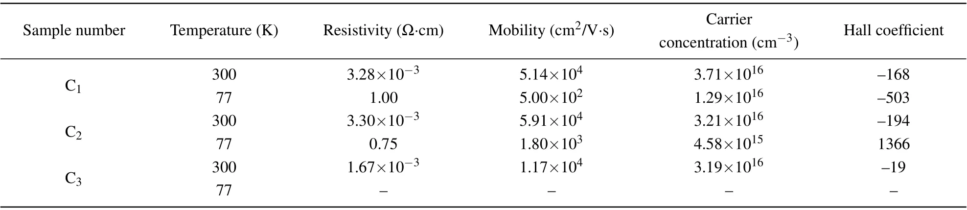
Table 1. Hall characterization of InSb samples with different buffer layers.
4. Conclusions
A compound buffer layer of InSb heterostructure has been successfully grown on GaAs(001)substrate.The buffer layers consist of GaSb layer as the first intermediate buffer layer and AlInSb layer as the second intermediate buffer layer.The morphology of GaSb buffer layer is a typical pyramid-like structure. AFM and TEM images of the buffer layer confirm the effective dislocation filtering effect by introducing superlattice buffer layer into AlInSb buffer layer. The RMS roughness of the InSb thin film surface with superlattice buffer structure is 0.18 nm, and the FWHM of HRXRD diffraction peak is 248 arcsec. Besides, the electron mobility at room temperature (300 K) reaches 5.91×104cm2/V·s. These results indicate that the InSb thin films grown on this type of buffer layer has the best material quality.
猜你喜欢
杂志排行

Chinese Physics B的其它文章
- Novel traveling wave solutions and stability analysis of perturbed Kaup–Newell Schr¨odinger dynamical model and its applications∗
- A local refinement purely meshless scheme for time fractional nonlinear Schr¨odinger equation in irregular geometry region∗
- Coherent-driving-assisted quantum speedup in Markovian channels∗
- Quantifying entanglement in terms of an operational way∗
- Tunable ponderomotive squeezing in an optomechanical system with two coupled resonators∗
- State transfer on two-fold Cayley trees via quantum walks∗