Pressure effect on electronic and optical properties of BiI3: first-principles calculations
2019-04-29SHENChenHaiWANGGuangTao
SHEN Chen-Hai, WANG Guang-Tao
(College of Physics and Materials Science, Henan Normal University, Xinxiang 453007, China)
Abstract: Based on the density functional theory (DFT), the pressure effect on the structural, electronic and optical properties of BiI3 are investigated by using the full potential linearized augmented plane wave (FP-LAPW) method, considering the spin-orbit coupling (SOC) effects. The calculated band structures show an indirect band gap of 1.867 eV for BiI3 at 0 GPa, and the gap value decreases as pressure increases. Moreover, the applied pressure can enhance the optical absorption coefficients and photoconductivity of BiI3. Thanks to its high absorption coefficient with an value of about 4×105 cm-1 and photoconductivity with a value of 3×10³ Ω-1·cm-1 in the visible light at 0 GPa, the optical response indicates that BiI3 is an alternative materials as a photovoltaic application.
Key words: First-principles calculation; Structural property; Electronic structure; Optical property; High pressure
1 Introduction
In recent years, Bismuth tri-iodide (BiI3) attracted scientist’s attention as an important semiconductor material for room temperature gamma-ray detections[1-3]and photovoltaic absorber applications[4,5]. Podrazaetal.[6]and Matsumotoetal.[7]showed that BiI3can be applied as a radiation sensor in room temperature gamma-ray detectors, primarily due to its high effective atomic number (ZBi= 83,ZI= 53) and density (5.78 g/cm3), as well as its wide band gap value 1.67 eV. Gokhaleet.al[8]fabricated an radiation detectors using the single crystals grown from ultra-pure BiI3powder by the Physical Vapor Transport (PVT) technique and estimated that the electron mobility of BiI3is 433 ± 79 cm2/V. Moreover, Saitoetal.[9]also fabricated a radiation detector and estimated that the mobility-lifetime product isμeτe= 3.4-8.5×10⁻⁶cm2/V and the electron-hole pair creation energy is 5.8 eV. All the researches suggest that BiI3are promising candidates for detectors in the radiographic imaging or gamma ray spectroscopy.
Recently, some research groups investigated the optical properties of BiI3and applied it to photovoltaic devices. Brandtetal.[5]measured its optical band gap (1.8 eV), optical absorption and recombination lifetime by experiment methods and got an indirect band gap 1.73 eV by density-functional theory (DFT) calculation. Moreover, the band gap of BiI3has been studied by different computational methods[6,10,11]and its value ranges from 1.43 to 1.92 eV. The values of optical band gap measured and reported in some previous studies[3,12-15]vary from 1.72 eV to 2.03 eV. More recently, Lehneretal. found that layer binary BiI3can be used as the active layer in planar solar cell architectures[4]. Therefore, the above studies indicate that layer binary BiI3may have an important application in the future optoelectronic devices.
It is well known that strain can tune effectively the phase transition, electronic and optical properties. Sunetal.[16]investigated the structure transitions of BiI3under high pressure by first-principle calculations, and Devidasetal.[17]investigated the pressure-induced change in the structure and the electronic properties of BiI3by using a combination of experiment and first-principles calculations. However, to our knowledge, the pressure effects on band structures and optical properties of BiI3have not been investigated to date. In this work, we systematically investigate the electronic structures and optical properties of BiI3under different pressures by using first-principles calculations. Our results can provide a reference in theory for the future applications of BiI3in photovoltaic devices or optoelectronic devices.
2 Computation details
All the calculations were performed by FP-LAPW method as implemented in WIEN2k package[18,19]. The exchange-correlation functional employed generalized gradient approximation in the Perdew-Burke-Ernzerhof form (GGA-PBE)[20]. All the geometry structures of BIi3were fully relaxed with SOC until force were converged to 1.0 mRy/Bohr. We used a parameterRMTKmax=7, whereRMTdenotes the minimum radius of the muffin-tin atomic sphere andKmaxis the magnitude of the greatestKvector in the plane wave expansion. Both theRMTof Bi and I are taken to be 2.5 Bohr. The modified tetrahedron method[21]was applied to integrate inside the Brillouin zone(BZ) with a dense mesh of 1000 uniformly distributed k-points. For the calculation of optical properties, we increased the numbers of k-point to 5000. The self-consistent was converged to 10-5eV.
The linear response of a material to an external electromagnetic field is measured by using the complex dielectric function:
ε(ω)=ε1(ω)+iε2(ω)
(1)
The imaginary partε2(ω) of the dielectric function could be calculated from the momentum matrix elements between the occupied and unoccupied wave functions with the selection rules[22]:
(2)
whereMcv(k) are the matrix elements of direct transitions between valence bandμvk(r) and conduction bandμck(r) states andωcv(k) =Eck-Evkis the corresponding transition energy.
The real partε1(ω) of the dielectric function can be evaluated from the imaginary part by Kramer-Kronig relationship[23]:
(3)
wherePis the principal value of the integral. All of the optical properties, including the absorption coefficienta(x), refractive indexn(x), extinction coefficient and the energy-loss spectrumL(x), can be directly calculated fromε1(ω) andε2(ω)[20,24].
3 Results and discussion
3.1 Structure parameters

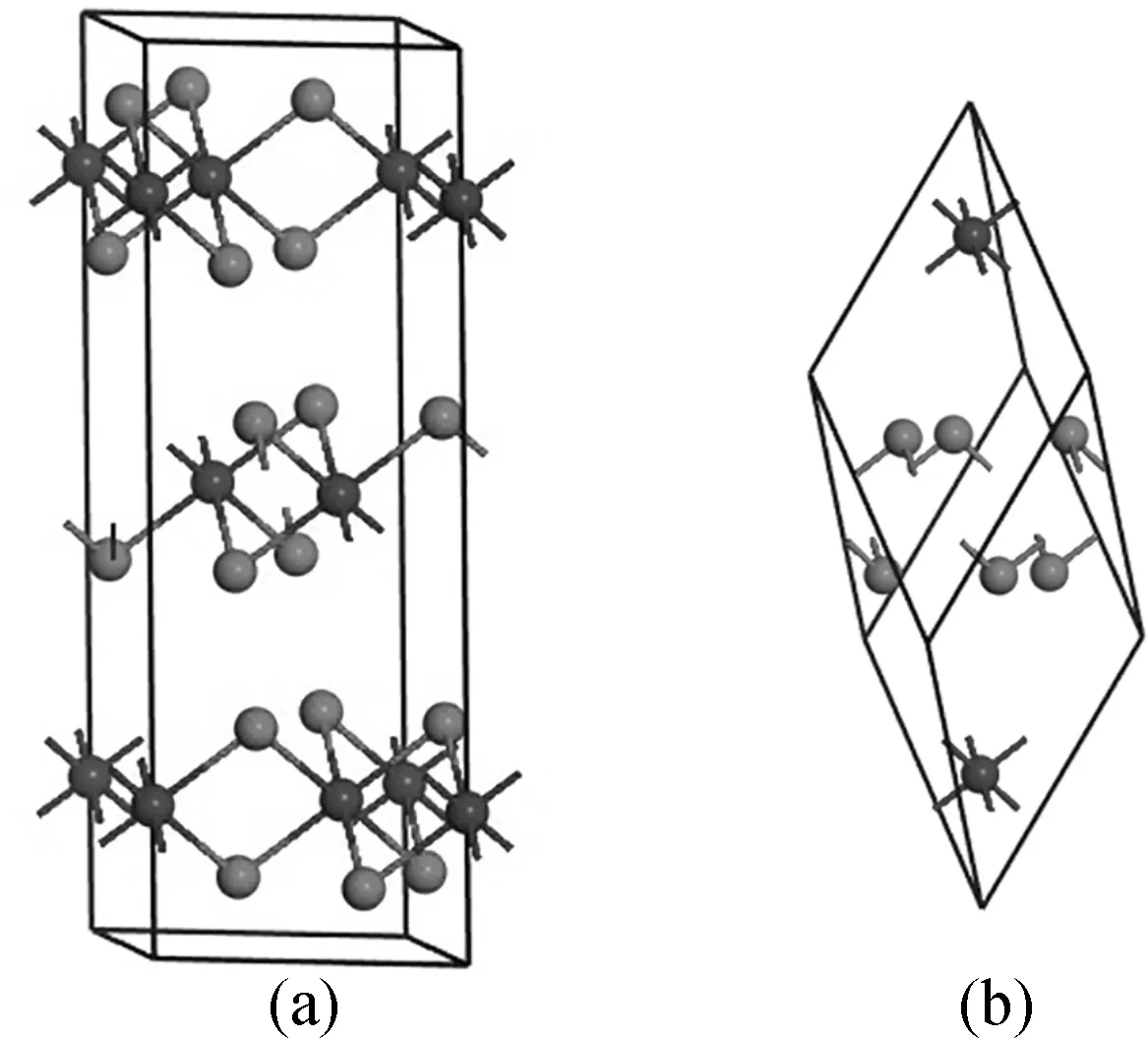
Fig. 1 (a) The unit cell and (b) primitive cell of BiI3, dark gray balls stand for Bi atoms and light gray balls for I atoms
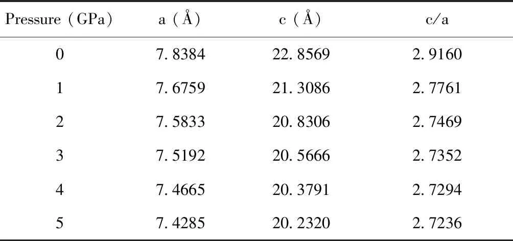
To make the calculations of the electronic and optical properties of BiI3more precise, the structure optimization is made by the following method. We select respectively five values with the form of percent change for the volume andc/aof BiI3, such as -6%, -3%, 0, 3% and 6% for volume change and -4%, -2%, 0, 2% and 4% forc/achange, to form a 2D mesh. The optimized structure can be found by calculation the total energy of the 25 points in the mesh with the relaxation of internal coordinates. The optimized structural parameters are listed in Table 1. Numerical results show that the calculated lattice parameters area=7.8384 Å andc=22.8569 Å, which agree with the experimental measuresa=7.823 Å andc=20.721 Å[25].
Next, we investigate the influences of different pressures on structure parameters of BiI3. We optimize thec/avalue for each considered pressure to obtain more accurate results in the future calculation for each property of BiI3. The total energy as a function ofc/aratio at different pressures is shown in Fig. 2. By fitting these data points and then finding the point corresponding to the minimum energy, the optimizedc/aat each pressure is obtained and shown in Fig. 3. The values of a, c andc/aeventually adopted by fitting these data are listed in Table 1. Numerical results show that the total energy increases with the increase of pressure applied to the BiI3. Moreover, the optimizedc/avalue at each pressure decreases with the increase of pressure. The reason can be understood as follows. Bulk BiI3has a layer structure, in which the van der Waals force between layers is week in comparison with the strong ionic bonding within a layer. Thus, the change of distance in the direction ofcaxis is more evident than that ofaaxis andbaxis in the BiI3. Moreover, Fig.3 also shows that there is a pressure point, 2 GPa, below which the value ofc/adecreases rapidly and above which it decreases slowly.
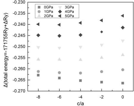
Fig. 2 The total energy as a function of c/a ratio at different pressures for BiI3 with R-3 phase
Table 1 The optimized lattice constants and the c/a ratios at different pressures
Pressure (GPa)a (Å)c (Å)c/a07.838422.85692.916017.675921.30862.776127.583320.83062.746937.519220.56662.735247.466520.37912.729457.428520.23202.7236

Fig. 3 Change of the optimized c/a with the increase pressure for BiI3 with R-3 phase
3.2 Pressure effects on electronic structures of BiI3
The calculated band structure of BiI3at 0 GPa is shown in Fig. 4(a) and the conventional Brillouin zone and k-path of BiI3are also shown in Fig.4(b). The band structures show that the conduction band minimum (CBM) is located at A point, while the valence band maximum (VBM) lies between A point and Γ point. The results indicate that BiI3possesses the indirect band gap characteristics with the band gap values of 1.867 eV, which agrees with previous studies[14]. In addition, our calculation results show that for the band structures of BiI3at different pressures, there are no obvious differences on the shape of conduction band and valence band at different pressures. However, compared with the gap value 1.867 eV at zero pressure, the calculated values of band gap are 1.731 eV at 1 GPa, 1.677 eV at 2 GPa, 1.626 eV at 3 GPa, 1.595 eV at 4 GPa and 1.572 eV at 5 GPa respectively, which indicates that the gap value is decreased when the applied pressure is increased, as shown in Fig. 4(c).
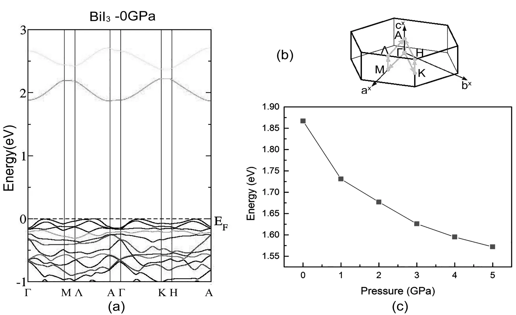
Fig. 4 (a) The calculated band structure of BiI3 at 0 GPa, (b) the conventional Brillouin zone and k-path of BiI3 and (c) the band gap energy of BiI3 at different pressures.
Fig. 5 shows the total and partial densities of state (DOSs) of BiI3at different pressures. Numerical results show that for the applied pressures ranging from 0 GPa to 5 GPa, the electronic characteristics present similar behavior. Moreover, the electronic states are separated into three regions: lower energy region between -12 eV and -8 eV mainly is contributed by Bi-s states; the energy region between -4 eV and 0 eV mainly attribute to the mixing hybridization between I-p states and Bi-s states. Meanwhile, the CBM is dominated by Bi-p states with little contribution of I-p states.
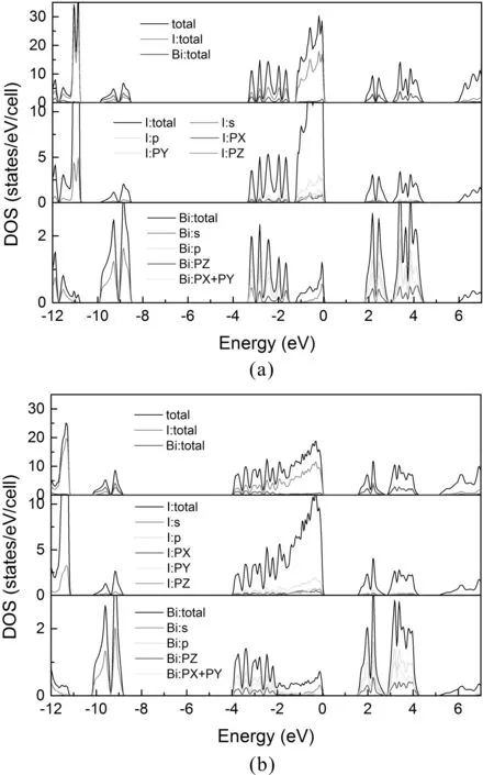
Fig. 5 Total and partial density of states for BiI3 at (a) 0 GPa and (b) 5 GPa. The Fermi level is set to zero
3.3 Pressure effects on optical properties of BiI3
It is well known that the optical properties of semiconductor material are very important to the optoelectronic device applications. Thus, in this subsection, we will investigate the influences of pressure on optical properties of BiI3, such as the imaginary partε2(ω) and real partε1(ω) of dielectric function, and optical absorption coefficient. Moreover, the optical properties along a- and c-axes are denoted as xx and zz.
In Fig. 6, we present the real partsε1(ω) and imaginary partsε2(ω) of dielectric function for BiI3along xy- and z-directions at different pressures. Numerical results show that the imaginary partsε2(ω) and real partε1(ω) present anisotropic characteristics in the BiI3. The reason is that the hexagonal structure of BiI3leads to a difference for the dielectric responses between thexyplane andz-direction. As is also well known, the static dielectric constantε1(0) is the most important parameter of the real partε1(ω) of the dielectric function, which may be related to the reflective index measured at a frequency above the lattice vibration frequencies. It can be seen from Fig. 6(a) that the value of static dielectric constant increases with the increase of pressure ranging from 0 GPa to 5 GPa. Moreover, Fig. 6(a) also shows that the value of real part of dielectric function increases with the increase of pressure when the photon energy is lower than 2 eV, while the change of the value of dielectric function is insensible when the photo energy is beyond 2 eV.
In addition, we can also see from Fig. 6(b) that for the imaginary partε2(ω), the threshold energy value decreases slightly with increasing pressure, which corresponds to the direct optical transition between the upper of the valence band and the lowest conduction band level. The reason is that the band gap is decreased when the pressure is increased. In addition, Fig. 6(b) also further shows that the imaginary part of dielectric function of BiI3increases with the increase of pressure. The strong relationship betweenε1(0) andEgcan be explained from the basis of Penn Model[26],ε1(0)=1+(ħω/Eg)2, where the static dielectric constant changes inversely with the value of band gap.

Fig. 6 The calculated (a) real part, (b) imaginary part of dielectric function, absorption coefficient with (c)electromagnetic field perpendicular to c axis and (d) electromagnetic field parallel to c axis for BiI3
To further understand the pressure effects on opticalproperties, the optical absorption coefficients are investigated as a function of photon energy at different pressures and along different incident light polarization directions, which are shown in Fig.6 (c) and (d). Numerical results show that the characteristics of thexyplane andz-direction optical absorption coefficients are different for each considered pressure, which further indicates that the optical absorptions are anisotropic in the BiI3material. In addition, it can also be seen from Fig.6(c) and (d) that with the increase of pressure, the red shift of the absorption edge occurs for both thexyplane andz-direction polarization cases, which is the results of decreasing band gap. Also, the values of optical band gap is 1.76 eV at 0 GPa, 1.68 eV at 1 GPa, 1.64 eV at 2 GPa, 1.60 eV at 3 GPa, 1.59 eV at 4 GPa and 1.58 eV at 5 GPa, respectively. Fig. 6(c) and (d) shows that the decreases of band gap induce the increases of optical absorption strength of ~105cm-1in the visible light activity range. These results indicate that BiI3is expected to be a promising material in optoelectronic devices.
In Fig. 7, we also present the photoconductivity,σ(ω), as a function of photon energy, considering different pressures and incident light polarization directions. The optical conductivity parameters are closely related to the photo-electric conversion efficiency and mainly used to measure the change caused by the illumination. Numerical results show that BiI3has non-vanishing conductivity in the visible light region (about 1.62-3.11 eV), and hence has a strong absorption ability to solar radiations. All of these factors mentioned above are a powerful suggestion that BiI3can be used to make thin-film solar cell, and Lehneretal[4]have fabricated solar cell with efficiency approximately 0.3% using BiI3as active layer. Thus, the results also further indicate that BiI3has a potential application to fabricate optoelectronic devices under high pressure.
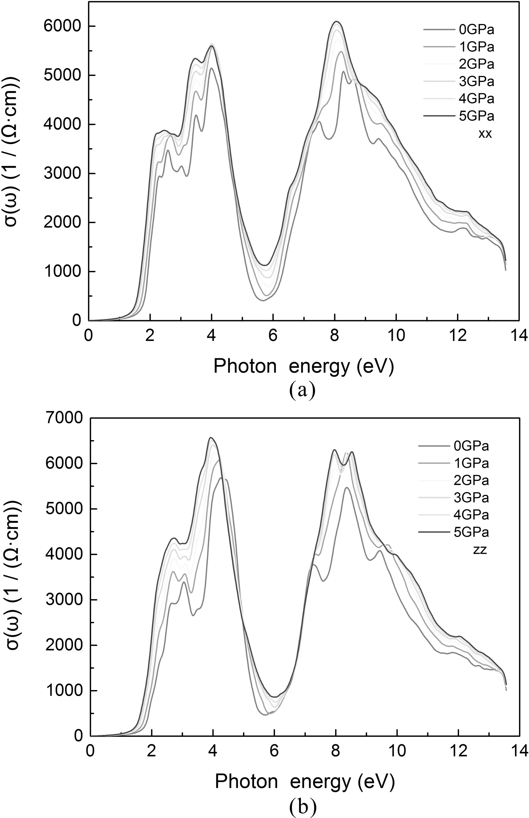
Fig. 7 The calculated photoconductivity for BiI3 with (a) electromagnetic field perpendicular to c axis and (b) electromagnetic field parallel to c axis.
4 Conclusions
We have investigated the pressure effects on structural parameters, electronic structures and optical properties of BiI3by using the first-principles method. Numerical results show that the band gap value of BiI3decreases as pressure increases. Moreover, its optical properties present the anisotropic characteristics for each considered pressure case. The static dielectric constant increases with the increase of pressure. The real part of dielectric increases when photon energy is lower than 2 eV, while it is insensible when the photo energy is beyond 2 eV at different pressure. Also, the pressure also induces the red shift of the threshold energy values of imaginary part and optical absorption. In addition, our results also show that high optical absorption strength (of ~105cm-1) and non-vanishing conductivity occur in the visible light activity range. These results also further indicate that BiI3has a potential application to fabricate optoelectronic devices under high pressure.
