Characterization of Self-driven Cascode-Configuration Synchronous Rectifiers
2019-03-07RENXiaoyongLIKunqiCHENQianhong
REN Xiaoyong,LIKunqi,CHEN Qianhong
Aero-Power Sci-Tech Center,College of Automation Engineering,Nanjing University of Aeronautics and Astronautics,Nanjing 210016,P.R.China
Abstract:This paper presents a cascode configuration synchronous rectifier device based on silicon MOSFET and Schottky diode,which can replace traditional power diode directly.This structure has self-driven ability with simple external circuit,and the conduction characteristic is preferable to a power diode.Static characterization and switching behavior analysis of proposed structure are conducted in this paper.The switching process is illustrated in detail using real model which considers the parasitic inductances and the nonlinearity of junction capacitors.The real time internal voltage and current value during switching transition are deduced with the equivalent circuit.To validate the analysis,two voltage specification rectifiers are built.Finally,double-pulse test results and the practical design example verify the performance advantages of proposed structure.
Key words:synchronous rectifier(SR);self-driven;cascode structure;power diode
0 Introduction
Synchronous rectifiers(SR)technology is an important method to improve converter efficiency,in which power MOSFETs take the place of diode as the rectifier to reduce conduction losses[1-4].Generally there are two types of driving methods:external-controlled methodsand self-driven methods.Selfdriven methods develop a SR driving signal from the voltage signal,which exists in the switching topology and coincides with the desired drive timing[5-9].It is simple and effective,however some topologies such as LLC resonant converter can hardly realize self-driven[10-11].Therefore,external driving signals are generated by detecting either the current through the field effect transistor(FET)or the voltage drop across the FET[10-16].Though it works well,the driver,the sampling and signal processing circuit increase the cost and complexity of the system.
In order to realize simple driver of SR,some new methods of self-driven SR based cascode structure which use SiC JFET and Si MOSFETs cascode with Si Schottky diode have been researched[17].It is used to replace front-end rectifier diode.Compared to the traditional external self-driver method,it is more effective and cheaper.But the additional circuit of this structure also has more components,which means it is hard to integrate all components in one package.
This paper presents a cascode structure selfdriven rectifier with simplified additional driver circuit,which is called active diode(ACD).This structure can realize integrated package just like cascode GaN FET[18],which means it can replace power diode directly.Both static and transient characteristics of the proposed ACD are analyzed in detail,such as the forward conduction and reverse breakdown characteristic,and turn-on and turn-off transient processes.This paper is organized as follows:Section 1 describes the basic structure and static characteristic of ACD.The forward characteristics of different combinations are compared with traditional power diode in order to highlight the advantage of this structure;Section 2 analyzes the detailed switching process,reverse voltage distribution and the expressions of voltage and current at ACD during switching transition;Section 3 verifies the proposed structure with experimental results.Finally,some conclusions are outlined in Section 4.
1 Basic Structure and Static Characteristic of ACD
The structure of the proposed ACD is shown in Fig.1,which consists of MOSFET S1and Schottky diode D1.In this structure,D1is in series with S1to achieve the function of power diode.The cathode and anode terminals of the module are S1drain terminal and D1anode terminal,respectively.Bias capacitor Ccis connected to the S1gate terminal and D1anode terminal to provide S1driving voltage.Transient voltage suppressor diodes DZ1and DZ2are in parallel with S1gate and source terminal to protect the S1gate from overvoltage and spikes.Compared to the fast recovery diode,Schottky diodes do not have reverse recovery period.Therefore in this structure D1usually uses Schottky diode to get the better dynamic performance.
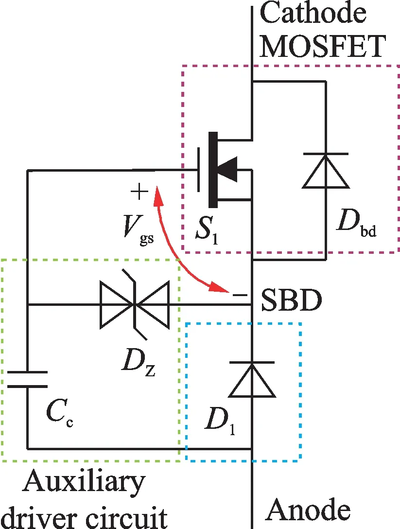
Fig.1 Basic structure and comportment of ACD
In the turn-off state,S1and D1sustain reverse voltage in series.Voltage distribution between two components is decided by turn-off transition process,which will be analyzed in next section.The peak repetitive reverse voltage of ACD VRRM_ACDis the total of the breakdown voltages of both D1and S1when the parameter is very well matched,such as

where VRRM_D1is peak repetitive reverse voltage of D1and V(BR)DSS_S1is drain-source breakdown voltage of S1.Usually the parameter of ACD can hardly be matched perfectly,therefore VRRM_ACDis definitely less than the sum of two reverse voltage as shown in Eq.(1).
In the turn-on state,Vgsis equal to Vc(ignore the voltage drop of D1).Forward current flows through the diode and MOSFET channel,the maximum forward current of ACD is the smaller one of D1maximum average forward current and S1continuous drain current,such as

The ACD forward voltage drop consists of the D1forward voltage drop Vf_D1and the S1on state resistance Rds_on,the relationship with current is

where ifis the forward current of ACD.The typical forward characteristic of ACD and two discrete devices are shown in Fig.2.With the forward current increasing,S1forward voltage drop increases linearly from zero,while D1forward voltage drop increases nonlinearly from an initial voltage.From Fig.2,it can be noted that,with respect to the forward current,the derivative of the S1forward voltage is larger than that of D1,leading to a crossover point in the figure.That is,before the crossover point,D1dominates the forward voltage drop.With the forward current further increasing,S1dominates the forward voltage drop,which makes the forward voltage of ACD has an approximately linear relationship with the forward current.
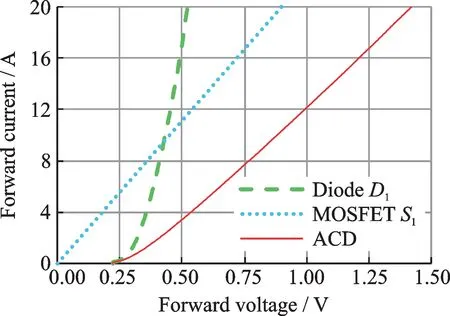
Fig.2 Forward characteristic of MOSFET,diode and ACD
Based on the aforementioned analysis,the forward voltage drop of ACD is determined by S1and D1.There are different combinations of S1and D1to construct the ACD with given specifications.In order to achieve better forward characteristics,it is necessary to find the optimal combination.In this section,two different specification power diodes are chosen to investigate the combination principle for better conduction performance.
Two popular voltage ratings are chosen to be evaluated.The first voltage specification type is a high voltage which VRRM_ACD=650 V.There are two combination types to realize this:600 V silicon carbide Schottky barrier diode(SiC SBD)cascaded with 55 V MOSFET or 60 V silicon Schottky barrier diode(Si SBD)cascaded with 600 V MOSFET.The forward characteristic of these two types and traditional power diode are shown in Fig.3.It is obvious that 600 V MOS cascaded with 60 V Si SBD has better conduction characteristic.
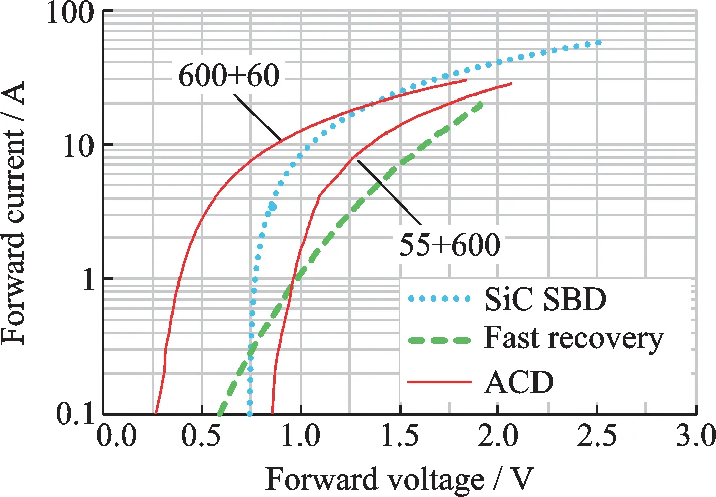
Fig.3 Forward characteristic comparison of two types of ACD with SiC SBD and fast recovery diode in 650 V
The second voltage specification type is a low voltage which VRRM_ACD=200 V.There are a variety of voltage specification devices to realize such combination.The forward characteristics of four typical combination types and traditional power diode are shown in Fig.4.
As can be seen in Fig.4,the lower the MOSFET voltage level is,the higher ACD forward voltage drop will be.Therefore,MOSFET voltage rating approaching the ACD voltage rating is preferred for better forward performance.Such a combination can also achieve low threshold voltage and dynamic resistance besides the excellent forward characteristics.

Fig.4 Forward characteristic comparison of four types of ACD with 150 V Si SBD and fast recovery diode
2 Analysis of Switching Behavior and Dynamic Characteristic
In this section,the detailed ACD switching mode analysis is presented based on the double pulse test(DPT)together with simulation results.The test setup is shown in Fig.5.To accurately measure forward current if,the device-under-test(DUT)and inductive load Lfare placed at the low side.The proposed analytical model includes the most parasitic parameters in actual device:parasitic inductors and capacitors.The symbol and reference direction of current and voltage are also marked in Fig.5.

Fig.5 Simulation circuit and analysis module of ACD
2.1 ACD turn-off transition switching behavior and voltage distribution
The voltage distribution between S1and D1is very important,which determines the reliability of proposed ACD.It is necessary to analyze the turnoff transition and find the relationship of Vdand Vds.
The key waveforms during turn-off transition are shown in Fig.6.Before Stturns on,the inductive load current ILtransfers from ACD to St,ifdecreases linearly and the slope depends on the value of Rg.When ifdecreases to zero,the turn-off transition begins.This transition can be divided into four stages.The detailed analysis is given in the following part.
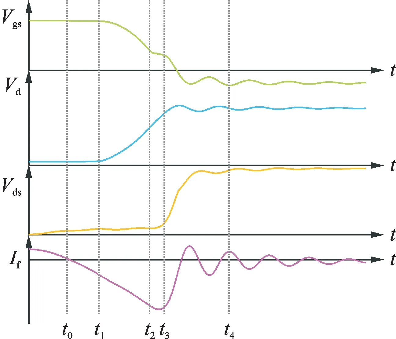
Fig.6 Key waveforms of ACD during turn-off transition
(1)Stage I:Diode reverse recovery delay period[t0,t1]
After ifdecreases to zero at t0,diode D1can hardly turn off immediately due to the energy storage effect of PN junction.During this period,diode current reversely increases to discharge D1junction energy.Therefore,S1and D1are entire conduction(as shown in Fig.7),the forward current if,which equals to id,reversely increases with the same slope of that before t0.Since D1uses Schottky diode in this structure normally,the reverse recovery process is usually around a few nanoseconds.This period ends when diode reverse recovery process finishes at t1.
(2)Stage II:Diode turns-off and MOSFET gate driver delay period[t1,t2]
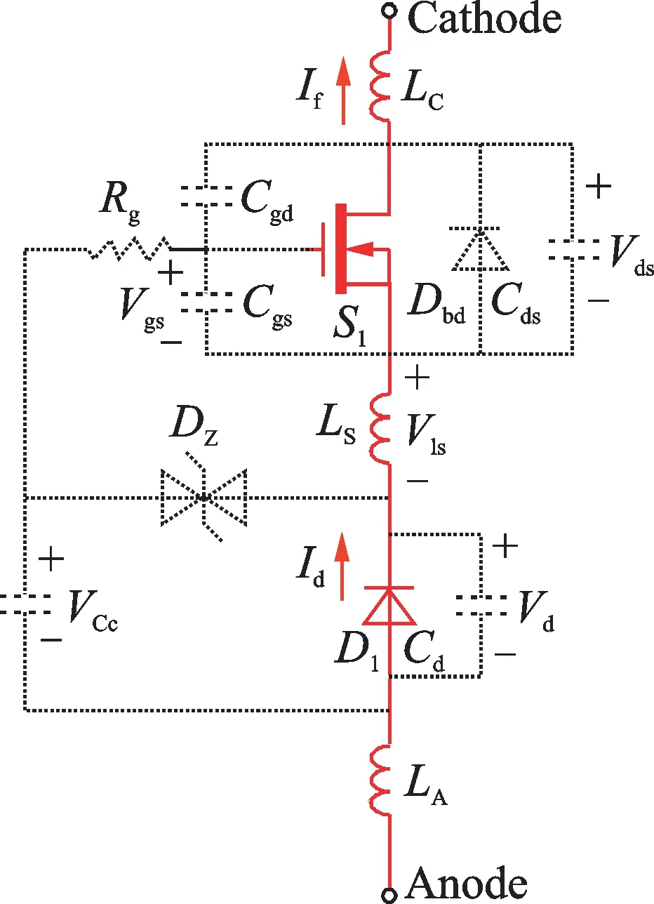
Fig.7 Equivalent circuit of ACD during turn-off stage I
When reverse recovery process finishes at t1,D1turns off and idflows through the junction capacitor Cdto charge it,then the reverse voltage of D1,Vdincreases.Due to gate capacitor Cgsof S1,Vgswill be still higher than miller voltage,S1keeps on in this period(as shown in Fig.8).The Kirchhoff voltage equation for this circuit is given below,which are composed of Cc,Cgs,Cdand Ls

Due to tiny parasitic inductance Ls,Vlsis negligible.With the S1driving voltage Vgsdecreasing at this period,Vdincreases.Accordingly,igflows through Cgsand Ccin single circuit path.Above is the self-driven mechanism of this structure.To analyze this period equivalent circuit in complex frequency domain,the equations are expressed as follow
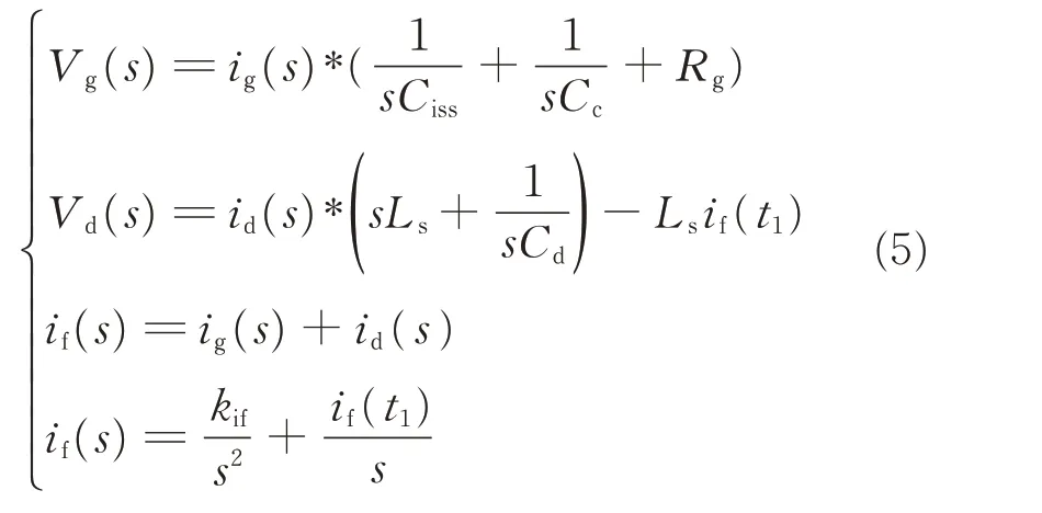
In this period,ifreversely increases with the same slope in stage I as S1still conducts.After solving Eq.(5),ig(s)and id(s)are

where a=CissCcCdLs,b=CissCCCdRg,c=CissCc+CissCd+CcCd.With the help of Generalized Ohm’s law,the voltage expression of this circuit can be found then.This period ends when Vgsdrops to the miller voltage at t2.
(3)Stage III:Main transition period[t2,t3]
When t=t2,Vgsdecreases to the miller platform,the operation state of MOSFET channel transits from the saturation-on state to linear state.The channel current iCHis determined by Vgs.With Vgsdecreasing,iCHwill decrease either.Then the excess forward current flows through Cdsto charge it.Therefore,the voltage Vdsincreases.The equivalent circuit of this stage is shown in Fig.9 and the current flowing through ACD satisfies
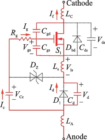
Fig.8 Equivalent circuit of ACD during turn-off stage II

Since Cgdis much smaller than Cdsfor most types of MOSFET,igdis much smaller than idswhich causes the voltage change of two capacitors is nearly same during this period.To simplify the analysis,igdis ignored in following analysis.The complex frequency domain equations at this period are
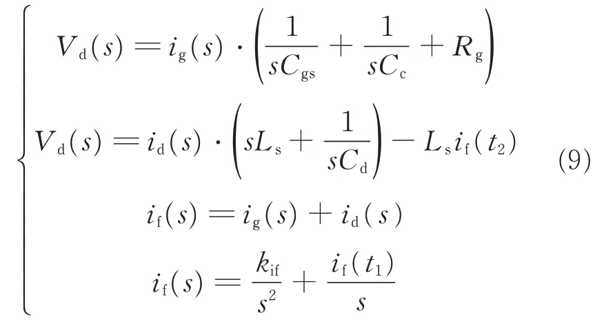
In this stage,the channel of MOSFET is in linear on state,and ifincreases with almost the same slope as in stage II.After solving Eq.(9),ig(s)and id(s)can be expressed as follows

where a=CgsCcCdLs,b=CgsCCCdRg,c=CgsCc+CgsCd+CcCd.According to the time domain analysis,the voltage and current of this circuit can be expressed as
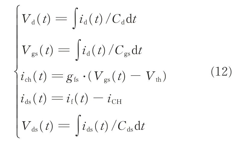
According to Eqs.(10)—(12),the time domain expression of Vd(t)and Vgs(t)can be found.Therefore Vds(t)can also be deduced with KVL equation.In this stage,ichcontinuously decreases with Vgsdecreasing.When ichdecreases to zero at t3,which presumes that Vgsdecreases below the S1threshold voltage,the channel of MOSFET is cutoff and this stage ends.

Fig.9 Equivalent circuit of ACD during turn-off stage III
(4)Stage IV:Remaining transition period[t3,t4]
At t3,Vgsdecreases below Vthand S1channel is cut off.All S1current flows into Cdspatch and charges it(as shown in Fig.10).In this period,all forward current ifdischarges parasitic capacitor for ACD.The expression of ifis

where Z is the equivalent complex impedance of ACD in this period,which can be expressed as

Fig.10 Equivalent circuit of ACD during turn-off stage IV

According to Eq.(13),the expression of if(s)in this period can be deduced.Then the expression of Vds,Vdand Vgscan be found from Eqs.(10)—(12).This period ends when Vcaequals to Vinat t4,and the whole turn-off transition finishes.
2.2 ACD tur n-on transition switching behavior
Before the ACD turns on,the current through ACD is zero,and the voltage of ACD is Vin.The turn-on transition can also be divided into four stages,and the key waveforms of turn-on period are shown in Fig.11.

Fig.11 Key waveform of ACD during turn-on transition
(1)Stage I:MOSFET drain-source voltage falling period[t0,t1]
As top switch in DPT circuit begins to turnoff,the inductor current ILtransfers from Stto the ACD and discharges Cdand Cds.Then Vdand Vdsdecrease immediately.Fig.12(a)shows the equivalent circuit of this stage.Based on the relationship in Eq.(4),Vgswill increase with the decrease of Vd.The circuit module of this period is the same as turnoff process stage IV,the voltage and current expression of this stage are also the same as Eqs.(9)—(12).This stage ends when Vdsdecreases to zero.
(2)Stage II:MOSFET body diode conduction period[t1,t2]
At t1,Vdsdrops to zero before Vgsincreases to the threshold value,the body diode Dbdof MOSFET turns on to freewheel inductor current IL.The equivalent circuit of this stage is shown in Fig.12(b),which is similar to turn-off stage II.Then the voltage and current expression of this stage still are the same as Eqs.(5)—(7).This stage ends when Vgsrises to MOSFET threshold voltage Vgs_that t2.
(3)Stage III:MOSFET current transform period[t2,t3]
When Vgsreaches Vgs_that t2,S1turns on and freewheeling current transfers from MOSFET body diode to channel.The equivalent circuit of this stage is shown in Fig.12(c).At this stage the circuit module is similar to that in the last stage,the only difference is the current transform process,which has no impact on the charge relationship of junction capacitor.Therefore,the current and voltage expression is same as last stage.This stage ends when Vgsrises to miller platform,which means that all the freewheeling current flows through S1channel.
(4)Stage IV:Diode junction capacitor discharge period[t3,t4]

Fig.12 Equivalent circuits of ACD during turn-on stage
When Vgsreaches miller platform at t4,S1fully turns on,then the freewheeling current discharges diode junction capacitor Cdand Vddecreases.The equivalent circuit of this stage is shown in Fig.12(d),which is still similar to that in the previous stage.Then the current and voltage expressions are the same as those in the last stage too.When Vddrops to zero,the whole turn-on transition ends and ACD transforms from turn-off state to turn-on state.After the ACD fully turns on,the inductor current ILflows through the channel of MOSFET and diode,Vgsis clamped by bias capacitor voltage Vc,which maintains on state of MOSFET.
3 Experimental Results and Discussion
To verify the feasibility of proposed ACD,a double-pulse test setup is built in lab.Operation waveforms and voltage distribution are investigated.Additionally,a DC-DC prototype is also built to evaluate the performance of the proposed ACD.
3.1 Double-pulse-test waveform verification
Fig.13 shows the prototype of the double-pulse test circuit.The top switch is a high voltage silicon transistor driven with silicon-lab high performance isolated driver SI8261.The coaxial shunt resistor,which has high bandwidth and minimized parasitic inductance,is adopted to improve current measure accuracy.
Fig.14 shows the prototype of proposed ACD.Bias capacitor uses a high stability C0G material ceramic capacitor to make sure capacitance is constant under any reverse voltage and temperature.Two typical voltage-level ACDs are established to verify the voltage distribution and dynamic process in this paper.

Fig.13 Prototype of double-pulse test circuit

Fig.14 Prototype of ACD
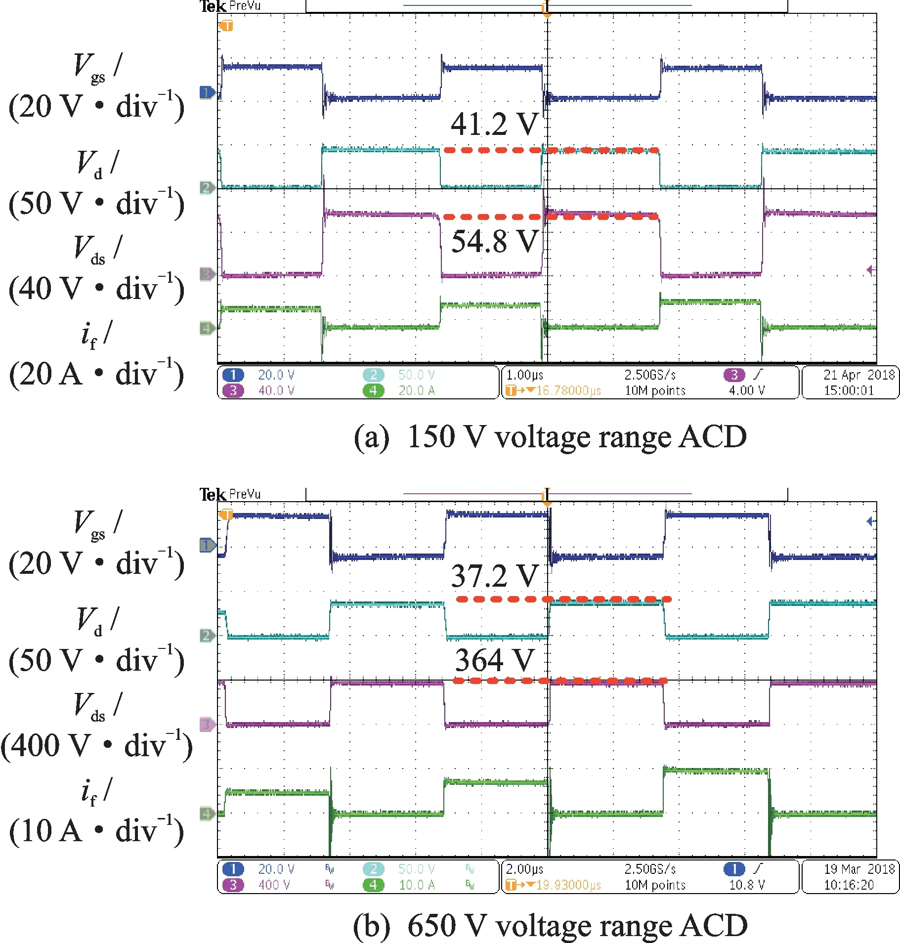
Fig.15 Experimental result of double-pulse test circuit
Fig.15 shows the steady-state experimental waveforms of two kinds of ACD,which include driver voltage Vgs,diode reverse voltage Vd,MOSFET drain-source voltage Vdsand forward current if.The input voltages of these two ACDs are 100 V and 400 V,respectively.The average inductor current is 10 A.The experimental results show that these two ACDs can realize self-driven function,and the driver voltage Vgscan be clamped to a suitable value by TVS.
Fig.16 shows the forward characteristic of two types of ACD compared with same specification power diode by double pulse test.As can be seen,the ACD has a lower knee voltage and lower dynamic resistance.Therefore,the forward voltage drop of ACD is lower than power diode.
Fig.17 shows the voltage distribution comparison between the double-pulse test and calculated result of the proposed analytical function at Section III.Fig.17(a)is the result of 150 V ACD and Fig.17(b)is 650 V.The analytical function matches well with experimental results.

Fig.16 Experimental result of forward characteristic by ACD and traditional diode

Fig.17 Voltage distribution comparisons
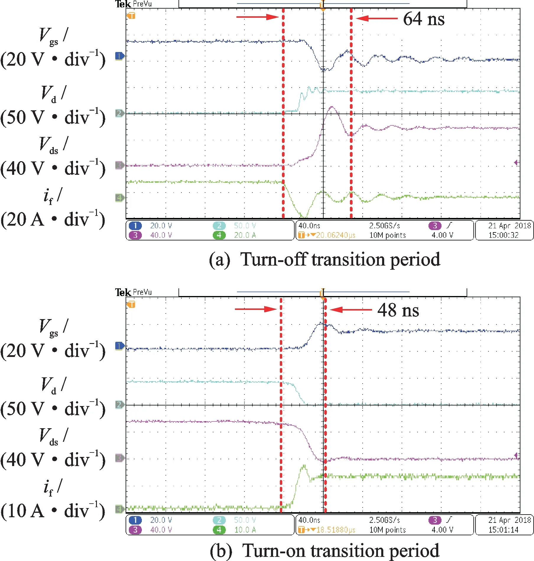
Fig.18 Transition waveform of 150 V voltage specification ACD

Fig.19 Transition waveform of 650 V voltage specification ACD
Fig.18 and Fig.19 show the double-pulse test transition waveforms of 150 V and 650 V ACDs,respectively.Fig.18(a)and Fig.19(a)are the turnoff transitions,while Fig.18(b)and Fig.19(b)are the turn-on transition.During the turn-off transition,when ifdrops to zero,Vdincreases immediately as Vgsdecreases.Vdsincreases when Vgsdecreases below the threshold value.During the turn-on transition,Vdsand Vddecrease in common with ifincreases and Vgsincreases with Vddrops.When Vgsincreases to the threshold value,Vdsdrops to zero approximately.The 650 V ACD is more obvious,for high voltage MOSFET has smaller Cdsat high drain-source voltage.After some time delay Vdand Vdsdrop to zero and Vgsreaches to the high value,then the MOSFET fully turns on.The whole turnoff and turn-on transition process are consistent with the analysis in Section III.The only difference is voltage and current have a ringing period at the end of the transition process.The ringing in forward current is a normal phenomenon at turn-off period.The reason of this ringing is that the parasitic inductor will resonant with the junction capacitor.For the consideration of efficiency,ACD needs to decrease the parasitic inductance.
3.2 Experimental results in LLC converter secondary-rectifier circuit with ACD
To evaluate the performance of proposed ACD in high operation frequency,a LLC resonant converter is developed in Fig.20.

Fig.20 Topology of LLC converter with ACD
The primary inverter and secondary rectifier both use the full-bridge circuit.Table 1 shows the circuit parameters.In the prototype,the 650 V ACD is used to replace the secondary rectifier diode.

Table 1 Circuit parameters of experimental prototype
Fig.21 gives the steady-state waveforms of LLC converter with ACD.It can be seen that ACD realizes the function of the diode.And some reverse recovery current is used to provide the driving energy.

Fig.21 Steady-state waveforms of LLC converter with ACD
Fig.22 shows an efficiency comparison between the proposed 650 V ACD and the traditional 650 V fast recovery diode DSEP-2906A in the LLC converters with the same specifications.The efficiency of proposed ACD is 0.2%lower than traditional power diode DSEP-2906A in full load condition.The reason for this result is that ACD is built with discrete devices soldering on PCB.It introduces multiple parasitic inductances,which will definitely result in long time damping of voltage and current at switching transition process,leading to higher switching loss[18].With two-die co-package structure,the performance should be much better than this discrete device structure.To verify this result,Fig.22 also gets the simulation result with co-package parasitic parameter ACD.It can be seen that with co-package,the efficiency benefit of ACD is obvious in full load range.
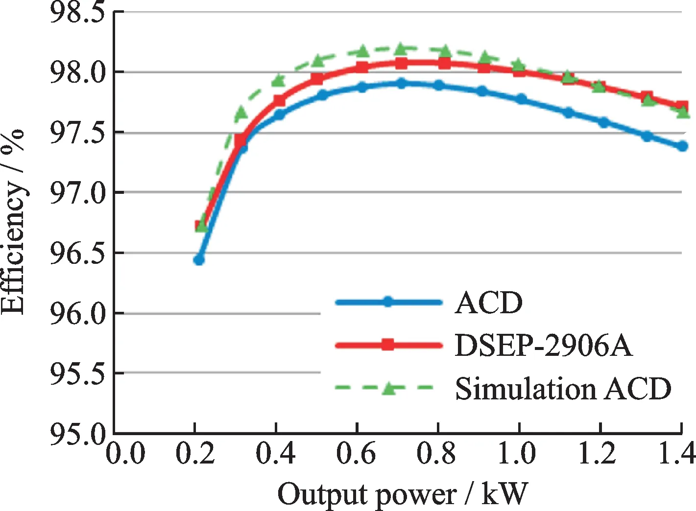
Fig.22 Efficiency comparison between ACD and the fast recovery diode in LLC converter
4 Conclusions
This paper proposes the ACD based on silicon MOSFET and Schottky diode,which can replace traditional power diode directly.The forward characteristic analysis has been conducted to show that the conduction loss of ACD is less than power diode.To evaluate the dynamic characteristic,switching behavior analysis is also given.Based on that,the double-pulse test is applied to verify the analytical characteristic and switching behavior.Finally,practical design with the proposed ACD in a LLC converter is finished in lab.The results show that the proposed ACD is practical,and it can realize high performance self-driven synchronous rectification with low cost.And if with a real co-package,the performance will be even better.
杂志排行
Transactions of Nanjing University of Aeronautics and Astronautics的其它文章
- BeiDou B1I/B3I Signals Joint Tracking Algorithm Based on Kalman Filter
- Impact Analysis of Solar Irradiance Change on Precision Orbit Determination of Navigation Satellites
- Cooperative Search of UAV Swarm Based on Ant Colony Optimization with Artificial Potential Field
- H∞Preview Control for Automatic Carrier Landing
- Single-Phase to Three-Phase Inverter with Small DC-Link Capacitor for Motor Drive System
- Analysis of Flight Dynamics Characteristics of Tilt Quad Rotor with Partial Tilt-Wing
