Aluminum-Doped Zinc Oxide Thin Films Synthesized by Atomic Layer Deposition for Photocatalysis
2018-11-02,,,,,
, , , , ,
(1.State Key Laboratory for Modification of Chemical Fibers and Polymer Materials, College of Materials Science and Engineering, Donghua University, Shanghai 201620, China; 2.Department of Materials Science, Fudan University, Shanghai 200433, China; 3.College of Science, Donghua University, Shanghai 201620, China)
【Abstract】 Zinc oxide (ZnO) and aluminum-doped ZnO (AZO) thin films were fabricated by atomic layer deposition using porous polyurethane as a sacrificial template. ZnO and AZO were firstly deposited onto the surface of polyurethane porous template followed by a calcination at 500℃ in oxygen atmosphere. Three-dimensionally semiconductor porous structures as a replica of the sacrificial porous template were thus achieved. After pulverizing, the porous structures were broken into small pieces, which were then employed as photocatalysts. With increasing Al doping, the optical band gaps and the photocatalytic performance increase correspondingly.
【Key words】 atomic layer deposition; Al-doped ZnO; photocatalysis
1 Introduction
Semiconductor photocatalysis has received intensive attention in environmental purification owing to its simplicity, mild reaction conditions, and low energy consumption[1-2]. Transition metal oxide semiconductors such as TiO2, and ZnO have been extensively studied for applications in photocatalytic activity, lithium ion battery, chemical and biological sensors, and electronic devices[2-12]. ZnO has attracted considerable attention because of its low cost and non-toxic nature[1, 13-15]. TiO2is known to be the most active photocatalyst for organic oxidation. Some certain studies, however, have reported that ZnO exhibits a better activity in photocatalytic performance as compared with TiO2[16-18]. The high photocatalytic efficiency of ZnO is attributed to its higher ability to generate H2O2, more active sites and higher surface reactivity than TiO2[17,19]. However, it was claimed that ZnO as a photocatalyst has several drawbacks including low stability due to photocorrosion[1], the high recombination rate of photogenerated electron-hole pairs, and a low quantum yield in the photocatalytic reactions in aqueous solutions which have been obstructing commercialization of the photocatalytic materials[16]. Consequently, a growing interest is exhibiting in improving the photocatalytic activity of ZnO. The improvement ideas include morphological change in nano-scale, composites structure optimization, defect introduction, and doping with transition metal oxides[16,20-21]. Among them, Al-doped ZnO (AZO) has received considerable attention because of its unique physical and chemical properties and low costs[16,22-24].
In this study, Al doped ZnO thin films were explored in terms of materials preparation and their photocatalystic performance. In the exploration, the phase structure, energy band structure, electron conductive path and acceleration of electron movements caused by the doping were taken into considerations.
2 Experimental methods
2.1 Synthesis of oxide thin films
In this work, ZnO and AZO films were firstly prepared by atomic layered deposition (ALD) on porous polyurethane sacrificial template (67×20×3mm3). In the ALD, diethyl zinc (DEZ) was used as the precursor of Zn and mixed with water (H2O) as the reactants. Both DEZ and H2O were exposed to the ALD reactor via computer-controlled valves with pulse and purge time of 50 ms and 30s, respectively. In the case of AZO, Al2O3as a doped-layer was deposited within the same pulse and purge time. The Al source of the precursor is trimethyl aluminum (TMA). For all doping and no doping depositions, the ALD reactor temperature was set at 150℃, and the temperatures of the TMA, DEZ, and H2O precursor bottles were set at 60℃, 45℃, and 50℃, respectively. The thickness of the oxide film was controlled by the number of ALD cycles. In order to fabricate AZO thin film, a single layer of Al2O3was inserted between the ZnO cycles. Two AZO samples were fabricated. The structure of AZO1 is 5 loops of ZnO (40 cycles)/Al2O3(1 cycle), while the structure of AZO2is 10 loops of ZnO (20 cycles)/Al2O3(1 cycle). To achieve catalyst materials, the deposited sponges were calcined at 500℃ in oxygen atmosphere. Thisproccess was able to form the three-dimensionally porous structures composed of many small thin films or flakes due to the polyurethane template was carbonized and reacts with oxygen to forms CO2. Eventually a large amount of thin films (flakes) can be formed by manual pulverization of the three-dimensionally porous structures. Thin films were also deposited on quartz substrates for comparison.
2.2 Characterization
The thin films morphologies were imaged by scanning electron microscopy (SEM, Phenom world). The crystal structures of photocatalyst were tested by X-ray diffraction (XRD) on a D8 spectrometer of Advance Bruker AXS GMBH, using Cu Kα radiation with irradiations condition of 40kV and 40mA. X-ray photoelectron spectroscopy (XPS) experiments were carried out on a RBD upgraded PHI-5000C ESCA system (Perkin Elmer) with Mg Kα radiation and the X-ray anode was run at 150W. Optical properties of ZnO and AZO thin films on quartz glass substrate were evaluated by UV-Vis spectrophotometer (Shimadzu UV-2550 spectrometer).
2.3 Photocatalytic measurement
Photocatalytic performance of ZnO and AZO were measured by photodegradation of MO solution using UV-Vis spectrophotometer. The ZnO-based thin films with the weight of 0.0125g were placed in 50mL MO solution with an initial concentration of 10mg/L, which was kept in the dark for 30min to achieve the adsorption equilibrium, and then illuminated under the UV light irradiation of 200-W xenon lamp (Lanpu, China) with the distance of 50cm from the MO solution. The degradation of the MO was measured every 20min. The absorption intensity at the wavelength of 464nm is found to be the maximum absorption peak of MO, and the intensity was extracted to calculate the MO degradation.
3 Results and discussion
Figure 1 shows the fabrication schematic of ZnO and AZO thin films synthesized by ALD. In the process, the original porous polyurethane template (Fig.1(a)) was deposited by ZnO or AZO with ~200 ALD cycles (Fig.1(b)). To obtain pure photocatalyst, the deposited sponge was calcined in oxygen atmosphere at 500℃. Oxygen reacts with a carbonizable organic material to form CO2and flow out of the calcination chamber, which eventually causes the formation of three-dimensionally porous structures consisting of thin films (Fig.1(c)). These structures were then pulverized manually to form powder/thin films (Fig.1(d)). In the following photocatalytic applications, the thin films were employed as photocatalyst.
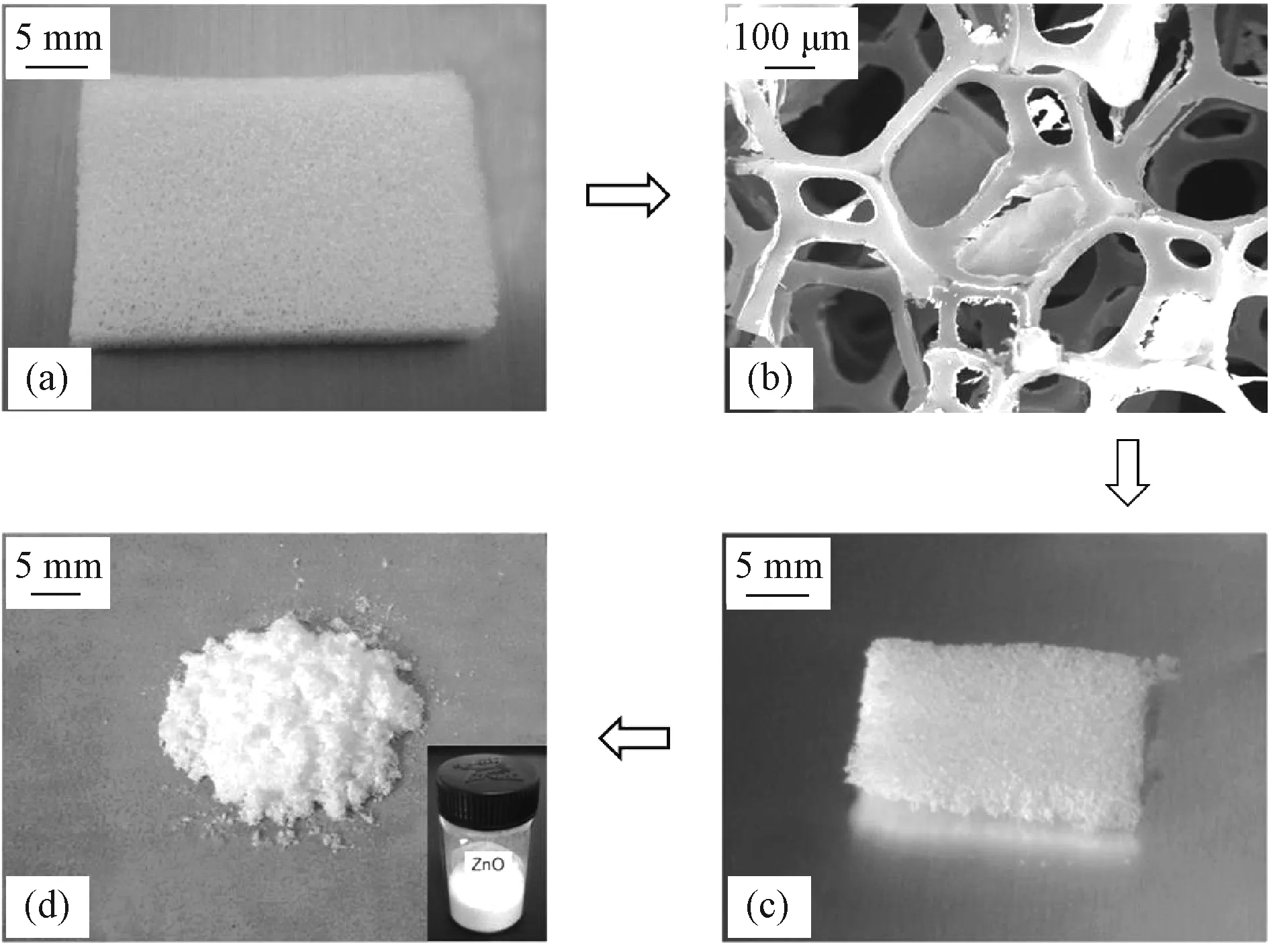
Fig.1 Fabrication schematic of ZnO and AZO thin films synthesized by ALD. (a) Photo of porous polyurethane template. (b) SEM image of the deposited template before calcination. (c) Photo of the thin film after calcination, (d) Powder/thin film formed after pulverization of the structure shown in Fig.1(c)

Fig.2 SEM images of (a) ZnO (200cycle), (b) AZO1 (ZnO(40)/Al2O3(1), 5 loops), (c) AZO2 (ZnO(20)/Al2O3(1), 10 loops), calcined at 500℃
Figure 2 show the SEM images of zinc oxide-based thin films of (a) ZnO (200 cycles), Al-doped zinc oxide of (b) AZO1 (ZnO(40)/Al2O3(1) 5 loops), and (c) AZO2 (ZnO(20)/Al2O3(1) 10 loops). The original structure consists of ZnO or AZO porous structure as a replica of the porous polyurethane template, which then was transformed into thin films by pulverizing process (Fig.2(a)~2(c)).
Figure 3 shows XRD patterns of ZnO and AZO thin films. It was shown that the strong and sharp peaks located at 2θ of 31.7, 34.4, and 36.2°, from (100), (002), and (101) planes, respectively of wurtzite structure of ZnO[1, 25-26]. Other peaks found at 2θ of 47.5, 56.6, 62.9, 66.4, 67.9, and 69.2° correspond to (102), (110), (103), (200), (112), and (201) planes, respectively[1, 26-29]. It clearly shown that there is no additional peaks due to the aluminum insertion, which indicates that the fabricated AZO are in single phase condition[1, 16]. The doping of ZnO thin film by replacing Zn2+with high valence atoms of Al3+leads to stress formation in the crystalline structure and is known to be responsible for deterioration in ZnO crystallinity[30-33]. As a result, AZO thin films show weaker crystallinity with reducing peak intensities[34-37], as shown in Figs. 3(b)~3(c). The feasibility of Al incorporation into ZnO implies the ability to control the crystallinity as well as tailoring of the band gap[37]. It has been known that the excess of the Al solubility limit in ZnO leads to Formation of ZnAl2O4with spinel-type structure[38-40], and indication of the formation of ZnAl2O4crystalline phase can be selected as the criterion for solid solubility limit[30, 41-42]. The current experimental results indicate that the AZO formed is still in the range of solid solubility limit.

Fig.3 XRD patterns of (a) ZnO (200 cycles) as well as AZO with various Al doping concentration of (b) AZO1 (ZnO(40)/Al2O3(1), 5 loops), (c) AZO2 (ZnO(20)/Al2O3(1), 10 loops)
Chemical compositions of Al-doped ZnO were measured by XPS. Figure 4 shows the XPS spectra of Zn, O, and Al of AZO thin films. It was shown in Fig.4(a) that the Zn 2p3/2and Zn 2p1/2peaks are almost the same for the two AZO samples, and the peak positions are ascribed to wurtzite structure[16,43]. Figure 4(b) shows the Gaussian deconvoluted XPS O 1s spectra of AZO thin films. The two peaks of O1 and O2 can be assigned to the Zn-O bond, and the Al-O bond/adsorbed oxygen, respectively[16, 34, 44-46]. The slightly shift in the two samples can be attributed to the different chemical environment because the Zn-O bonds are affected by the substitution of Al atoms at Zn sites[47]. Fig.4(c) shows the spectra of Al 2p of AZO thin films. It was shown that with increasing Al concentration the intensity of Al 2p peaks increases, and the Al atomic concentrations are calculated to be 1.3 % and 7.2 % for AZO1 and AZO2, respectively. The peak shifts to higher binding energy are believed to be due to more Al-O bonds[39].

Fig.4 XPS spectra of AZO1 (ZnO(40)/Al2O3(1), 5 loops), and AZO2 (ZnO(20)/Al2O3(1), 10 loops). (a) Zn 2p, (b) O 1s, and (c) Al 2p
Figure 5(a) shows the optical transmittance spectra of the ZnO and AZO thin films prepared on quartz substrates. It is shown that the optical transmittance of AZO thin films was slightly enhanced with increasing Al concentration, indicating that in the AZO, more facile electron transitions exist to absorb photons[48-49]. The optical absorption coefficient, α, can be calculated using Lambert’s equation[50-51]:
whereTis the optical transmittance andtis the thickness. The optical band gap (Eg) of ZnO and AZO can be evaluated by Tauc relation[47,52]:
αhν=A (hν-Eg)m
where A and hν are the proportionality constant and incident photon energy, respectively and m is a constant with the value is equal to 1/2 for a direct band gap semiconductor. The direct band gaps of the oxides can be estimated from the curve of (αhv)2-(hν) by extrapolating the linear region of the curves to intercept the x-axis[47,53], as shown in Fig.5(b). The estimated optical band gaps increase with increasing Al concentration as the values of the undoped ZnO, AZO1, and AZO2 are 3.13, 3.30, and 3.33eV, respectively. Here, the band gap of the ZnO (3.13eV) is in agreement to a reasonable extent with the accepted literature value of ~ 3.18 to 3.22eV[16,51,53-54]. The increase of the band gap with increasing Al doping is attributed to the Burstein-Moss effect, caused by an increase in free electron concentration due to Al doping[48,54-58]. ZnO thin films are naturally n-type oxide semiconductors due to natural electron donors generated by O vacancies and Zn interstitials[48]. The addition of donor Al3+cations raises the Fermi level of the AZO thin films into the conduction band, causing complete degeneration, and therefore the absorption edge moves to higher energy[48,55].
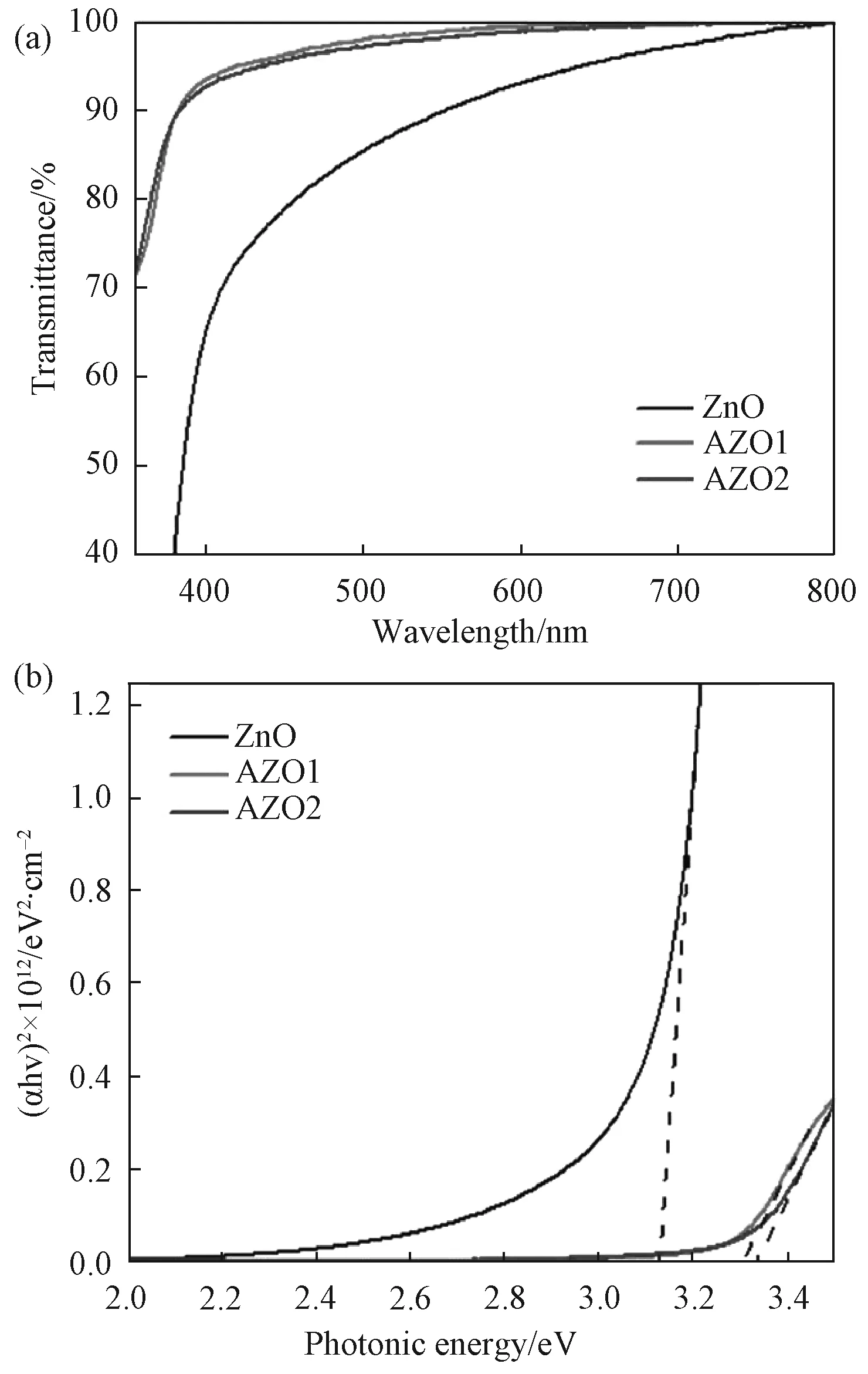
Fig.5 (a) Optical transmittance spectra, and (b) plots of (αhv)2against (hv) for ZnO (200 ALD cycles), AZO1 (ZnO(40)/Al2O3(1), 5 loops), and AZO2 (ZnO(20)/Al2O3(1), 10 loops)

Fig.6 (a) Photocatalytic performances of thin films: ZnO (200 ALD cycles), AZO1 (ZnO(40)/Al2O3(1), 5 loops), AZO2 (ZnO(20)/Al2O3(1), 10 loops). (b) Corresponding degradation rates, calculated from (a)
Figure 6(a) shows the photocatalytic performance of ZnO and AZO thin films annealed at 500℃ with MO solution used as a typical organic pollutant. The initial MO concentration is 10mg/L and ZnO or AZO photocatalysts concentration is 0.25mg/mL. It was shown that the presence of Al in ZnO gives a positive effect to the photocatalytic activities (Fig.6(a)). AZO thin films with higher Al doping concentration (AZO2) has a wider optical band gap (Fig.5(b)) and better photocatalytic performance than no and lower doping, e.g. ZnO (200 ALD cycles) and AZO1 in Figs.6(a) and 6(b). It can be explained as follows. The most important factor that can contribute to increase of photocatalytic activity is the presence of a high electric conductive phases, which leads to an increase of the probability of the carriers reaching the photocatalyst/solution interface[19,59]. When a small amount of Al was introduced into the ZnO thin film, the one ionized Al3+substitute for one Zn2+giving one free electron to the conduction band for every Zn2+site replaced by the Al3+[53,60-61], which eventually increases the conductivity[53]. In the photocatalysis respect, Al doping increased the photocatalytic activity by accelerating the transfer of electrons to dissolved oxygen molecules[1]. The recombination of the photo-generated carriers was effectively suppressed leading to an increase in the photo-oxidation efficiency[1].

ZnO/AZO+hν→e□+h+
(1)
H2O+h+→OH·+H+
(2)

(3)
(4)
(5)
(6)
OH·+dye → dye mineralization
(7)
4 Conclusion
ZnO and AZO thin films can be successfully deposited by ALD on porous polyurethane template. Calcination following the deposition makes the thin films form the three-dimensionally porous structures as a replica of the structure of original template. By pulverizing, the porous structures were broken into small pieces and form ZnO and AZO thin films. Experimental results show that the wurtzite crystal structure of ZnO can be maintained by Al doping, indicating a single phase structure. Furthermore, by presence and increasing of Al doping, the optical band gaps enlarges with the photocatalytic performance enhanced. The enlargement of optical band gap with increasing Al concentration is due to Al ions tending to occupy ZnO lattice planes, and consequently leading to the increase in transport path of charge carriers in ZnO lattice. The transport of photogenerated electrons to the outer systems will eventually be accelerated, resulting in high photocatalytic performance.
