高灵敏度Sb基量子阱2DEG的霍尔器件
2018-05-30武利翻苗瑞霞商世广
武利翻, 苗瑞霞, 商世广
(西安邮电大学 电子工程学院, 陕西 西安 710121)
1 Introduction
The Hall effect devices are by far the most widely used magnetic sensors today. Their future mainly depends on whether means will be deve-loped to enhance their sensitivity and improve their temperature stability. The use of two-dimensional electron gases (2DEG) already demonstrated to give the best compromise between high mobility and high carrier concentration while maintaining a reasonably high sheet resistance[1].
The criterion for a good material Hall magnetic sensors is a low carrier concentration and a high carrier mobility which is difficult to meet[2]. As a small band gap means a high intrinsic carrier density, InSb(Eg=0.18 eV) and InAs(Eg=0.36 eV) bulk crystals do not meet the criterion, especially above room temperature, although they have high carrier mobility. The majority of Hall magnetic sensors are made of Si and GaAs during the past decades. Their stability at high temperature and the possibility of using mature technology outweigh the drawback of small carrier mobility. As the epitaxy technology developed, InSb and InAs thin films were considered to produce Hall elements and the researchers made great progress[3-5]. The electrical and magnetic field characteristics of InSb thin films show a great difference from the bulk crystal. InAs films are a kind of promising material for magnetic sensors because of their larger band gap than InSb and higher electron mobility than GaAs[6-9].
In this paper, we report on a comparative study on the sensing performance and temperature stability of undoped and double δ-doped InAs/AlSb quantum well structures for the application in Hall sensors by MBE technology. Moreover, the influence of the measurement temperature on the sheet electron density and electron mobility is investigated.
2 Experiments
The Hall devices were grown on semi-insulating GaAs substrates by molecular beam epitaxy MBE. Nucleation layers of GaAs were firstly grown to ensure good starting conditions for the subsequent deposition of buffer layers of approximately 700 nm thickness. The standard buffer layer stack consists of AlGaSb that was followed by 50 nm AlSb. The buffer section was finished by growing a short-period smoothing superlattice. Finally, the InAs/AlSb quantum well structure was grown. The wafer was capped with dual layers of InAlAs and InAs, which placed the top of the InAs quantum well channel. The heterointerface was forced to be InSb like by using an appropriate shutter switching sequence. Hall mobilities and carrier concentrations were determined using van der Pauw method.
Two different layer samples were grown and processed. The schematic structures of two samples are shown in Fig.1. SampleⅠ is a conventionally undoped quantum well structure with an InAs quantum well thickness of 15 nm. Sample Ⅱ consists of double δ doping. Therst Si δ-doped layer is in-between undoped AlSb barrier and supply layers, which was grown after a lattice matched undoped 700 nm AlGaSb buffer layer. 15 nm InAs channel was grown as same as that of SampleⅠ, then highly tensile and undoped AlSb spacer with thickness of 5 nm was grown, followed by the second Si δ-doped layer. Wet chemical etching techniques were used for mesa isolation[10-11]. Afterwards, Ohmic contacts were made using Ti/Pt/Au metal. Fig.1 shows the cross sections of the sample Ⅰ and sample Ⅱ.
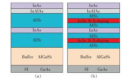
Fig.1 Schematic structure of Hall devices epitaxial layers. (a) Sample Ⅰ, unintentionally doped. (b) Sample Ⅱ, double δ-doped.
3 Results and Discussion
Two types of Hall devices were tested, shown in Tab.1. Sample Ⅰ represents a conventional Sb-based Hall device, and it is being used as reference in this study. Sample Ⅱ with the double δ-doped AlSb/InAs quantum well exhibits higher electron mobility and higher electron density. As the table shows, the room-temperature sensitivity of 96 mV·mA-1·kG-1·kΩ-1was achieved for the Hall devices based on the double Si-δ doped AlSb/InAs quantum well structure sample. The high mobility of the double δ-doped AlSb/InAs quantum well structure is advantageous to the high sensitivity for Hall devices. The higher sheet carrier concentration can improve the operation sensitivity. Thus, the double δ-doped AlSb/InAs quantum well structure for a Hall device is designed with the goal of improving its sensitivity.
To check the dominant scattering mechanism in determining the electron mobility in 2DEG layer, Hall measurements were performed from 77 K to 300 K on two samples. Electron mobility with high electron sheet density of 15 000 cm2·V-1·s-1with 4.52×10¹¹/cm2, and 16 000 cm2·V-1·s-1with 7.71×10¹²/cm2were achieved from epitaxial structure sample Ⅰ and Ⅱ at room temperature, respectively, employing van der Pauw Hall measurement. The measured results of samples Ⅰ and Ⅱ are listed in Tab.1. Fig.2 shows the measured electron mobilities from 77 K to 300 K as a function of different measurement temperatures. As can be seen from Fig.2, two distinct temperature dependences of electron mobility can be observed. From 300 K to 175 K, the electron mobilitiesvs. temperature for sample Ⅰ and Ⅱ shows identical variation trend and the acoustic phonon scattering is the dominant scattering, which results in all of them inT-3/2temperature dependence[12]. This also agrees very well with earlier reports from other researchers. However, in the temperature lower than about 175 K, the variation trends split and show obvious difference. At low temperature, the phonon scattering is weakened because of the weak vibration of atoms, thus the dominant scattering mechanism is the ionized impurity scattering, which shows the electron mobility will be only related toN-1doping concentration.
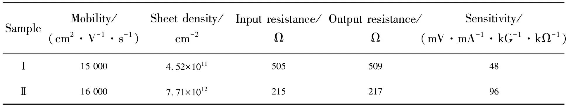
Tab.1 Characteristics of two samples of Hall devices
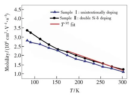
Fig.2 Electron mobility vs. temperature for sample Ⅰ and sample Ⅱ
In Fig.3, the sheet electron densities of these two samples are shown with measurement temperature from 300 K to 77 K. As can be seen from this figure, the sheet electron density keeps almost constant for the samples in different temperatures and becomes less temperature dependent, which indicates that high mobility two-dimensional electron gas does not consist of intrinsic electron generated in the channel by thermal-excitation. Otherwise, a sharp decrease of electron concentrations will be observed at 77 K as a result of the fact that most intrinsic electron is unionized at such low temperature range. Inserting double Si δ-doping on both sides of the quantum well, the sheet electron density up to 7.71×10¹²/cm2has been obtained.
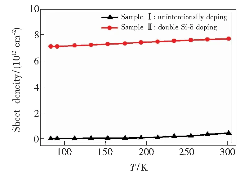
Fig.3 Sheet electron density vs. temperature for sample Ⅰ and sample Ⅱ
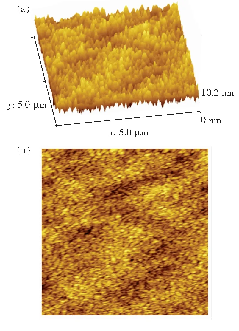
Fig.4 5 m×5 m AFM micrograph of sample Ⅱ.(a) Three-dimensional. (b) Two-dimensional.
4 Conclusion
In conclusion,two different InAs/AlSb heterostructure 2DEG-Hall devices with different doping concentrations were grown and characterized. Van der Pauw measurements show electron concentrations as high as 7.71×10¹²/cm2at room temperature. AFM measurement results show a smooth surface morphology and high crystalline quality of all the samples. Hall measurement shows that the electron mobility is limited by phonon scattering from 175 K to 300 K but is determined by the ionized impurity scattering below 175 K. The sheet electron density is almost independent with temperature from 77 K to 300 K. Moreover, further optimization of the double δ-doped AlSb/InAs quantum well structures growth should lead to an even better micro-Hall devices performance.
References:
[1] LI Y, XIONG P, MOLNR S,etal.. Hall magnetometry on a single iron nanoparticle [J].Appl.Phys.Lett., 2002, 80(24):4644-4646.
[2] DINGLE R, STORMER H L, GOSSARD A C,etal.. Electron mobilities in modulation-doped semiconductor heterojunction superlattices [J].Appl.Phys.Lett., 1978, 33(7):665-667.
[3] RIEDI S, REICH C, BERL M,etal.. Electron gas quality at various (110)-GaAs interfaces as benchmark for cleaved edge overgrowth [J].J.Cryst.Growth, 2016, 455(1):37-42.
[4] KUNETS V P, MAZUR Y I, SALAMO G J,etal.. Doped-channel micro-Hall devices: size and geometry effects [J].J.Appl.Phys., 2005, 98(20):094503-1-5.
[5] 朱彦旭, 王岳华, 宋会会, 等. 基于GaN基HEMT结构的传感器件研究进展 [J]. 发光学报, 2016, 37(12):1545-1553.
ZHU Y X, WANG Y H, SONG H H,etal.. Progress of sensor elements based on Ga-N HEMT structure [J].Chin.J.Lumin., 2016, 37(12):1545-1553. ( in Chinese)
[6] WU L F, ZHANG Y M, LV H L,etal.. Atomic-layer-deposited Al2O3and HfO2on InAlAs: a comparative study of interfacial and electrical characteristics [J].Chin.Phys. B, 2016, 25(10):108101-1-5.
[7] PIKULIN D I, HYART T. Interplay of exciton condensation and the quantum spin Hall effect in InAs/GaSb bilayers [J].Phys.Rev.Lett., 2014, 112(24):176403-6.
[8] YOKOYAMA T, TANAKA Y, INOUE J. Charge transport in two-dimensional electron gas/insulator/superconductor junctions with Rashba spin-orbit coupling [J].Phys.Rev. B, 2006, 74(3):035318-035324.
[9] WANG H M, ZENG Y P, FAN T W. Characteristics of InAs epilayers for Hall effect devices grown on GaAs substrates by MBE [J].J.Cryst.Growth, 1997, 179(12):658-660.
[10] ZHANG Y, ZHANG Y W, WANG C Y,etal.. High sensitivity Hall devices with AlSb/InAs quantum well structures [J].Chin.Phys. B, 2013, 22(5):057106-1-3.
[11] CHANG S Z, CHANG T C, LEE S C. The growth of highly mismatched InxGa1-xAs (0.28≤x≤1) on GaAs by molecular-beam epitaxy [J].J.Appl.Phys, 1993, 73(10):4916-4926.
[12] WANG J, XING J L, WEI X,etal.. Investigation of high hole mobility In0.41Ga0.59Sb/Al0.91Ga0.09Sb quantum well structures grown by molecular beam epitaxy [J].Appl.Phys.Lett., 2014, 104(5):052111-1-5.