Performance of dual-band short-or mid-wavelength infrared photodetectors based on InGaAsSb bulk materials and InAs/GaSb superlattices∗
2017-08-30YaoyaoSun孙姚耀YuexiLv吕粤希XiHan韩玺ChunyanGuo郭春妍ZhiJiang蒋志HongyueHao郝宏玥DongweiJiang蒋洞微GuoweiWang王国伟YingqiangXu徐应强andZhichuanNiu牛智川
Yao-yao Sun(孙姚耀),Yue-xi Lv(吕粤希),Xi Han(韩玺),Chun-yan Guo(郭春妍), Zhi Jiang(蒋志),Hong-yue Hao(郝宏玥),Dong-wei Jiang(蒋洞微), Guo-wei Wang(王国伟),Ying-qiang Xu(徐应强),and Zhi-chuan Niu(牛智川),†
1 State Key Laboratory for Superlattices and Microstructures,Institute of Semiconductors,Chinese Academy of Sciences,Beijing 100083,China
2 College of Materials Science and Opto-Electronic Technology,University of Chinese Academy of Sciences,Beijing 100049,China
3 Synergetic Innovation Center of Quantum Information and Quantum Physics,University of Science and Technology of China,Hefei 230026,China
Performance of dual-band short-or mid-wavelength infrared photodetectors based on InGaAsSb bulk materials and InAs/GaSb superlattices∗
Yao-yao Sun(孙姚耀)1,2,3,Yue-xi Lv(吕粤希)1,2,3,Xi Han(韩玺)1,2,3,Chun-yan Guo(郭春妍)1,2,3, Zhi Jiang(蒋志)1,2,3,Hong-yue Hao(郝宏玥)1,2,3,Dong-wei Jiang(蒋洞微)1,2,3, Guo-wei Wang(王国伟)1,2,3,Ying-qiang Xu(徐应强)1,2,3,and Zhi-chuan Niu(牛智川)1,2,3,†
1 State Key Laboratory for Superlattices and Microstructures,Institute of Semiconductors,Chinese Academy of Sciences,Beijing 100083,China
2 College of Materials Science and Opto-Electronic Technology,University of Chinese Academy of Sciences,Beijing 100049,China
3 Synergetic Innovation Center of Quantum Information and Quantum Physics,University of Science and Technology of China,Hefei 230026,China
In this paper,we demonstrate bias-selectable dual-band short-or mid-wavelength infrared photodetectors based on In0.24Ga0.76As0.21Sb0.79bulk materials and InAs/GaSb type-II superlattices with cutoff wavelengths of 2.2µm and 3.6µm, respectively.At 200 K,the short-wave channel exhibits a peak quantum efficiency of 42%and a dark current density of 5.93×10⁻⁵A/cm2at 500 mV,thereby providing a detectivity of 1.55×1011cm·Hz1/2/W.The mid-wave channel exhibits a peak quantum efficiency of 31%and a dark current density of 1.22×10⁻³A/cm2at−300 mV,thereby resulting in a detectivity of 2.71×1010cm·Hz1/2/W.Moreover,we discuss the band alignment and spectral cross-talk of the dual-band n-i-p-p-i-n structure.
short-/mid-wavelength,InGaAsSb,InAs/GaSb
1.Introduction
Short-wave infrared(SWIR)bands,from 1µm to 3µm, can offer high-resolution images comparable to visible perspective and exhibit the capacity to perform both passive and active imaging.Meanwhile,mid-wave infrared(MWIR) bands,corresponding to the atmospheric window between 3µm to 5µm,are widely utilized for military applications. Therefore,the combination of SWIR and MWIR is considerably essential and highly required in a number of tracking and reconnaissance missions.The dual-color SWIR–MWIR imagers permit more enhanced target identification and detection of chemical signatures specific to a waveband than singlecolor imagers.[1,2]
Bulk semiconductor materials,such as InGaAs for the SWIR and InSb for the MWIR,exhibit the advantages of high absorption coefficient and quantum efficiency.However, they are also limited to a particular detection window near the bandgap.[3]HgCdTe is a particular family that can tailor the cutoff wavelength from SWIR to considerably longwave infrared(VLWIR)by changing the molar fraction of Cd.However,it exhibits high cost and toxicity.[4,5]Quantum well infrared photodetectors(QWIPs)and quantum dot infrared photodetectors(QDIPs)are alternatives to infrared detection.However,they were proved to present lower quantum efficiency and larger dark current,which limit the frame rate and operating temperature of focal plane arrays.[6]Another feasible scheme is type-II superlattices(SLs)introduced by Esaki and Tsu.The detection range can also cover from SWIR to VLWIR by changing the relative thickness of alternate layers.Reports on the subject were published intensively within the past two decades based on traditional InAs/GaSb SLs and modified Ga-free SLs.[7–10]
The quaternary alloy In0.24Ga0.76As0.21Sb0.79,lattice matched to GaSb substrate,is a promising candidate for the optoelectronic devices in the short-wave range.During the past few years,InGaAsSb detectors were reported with different structures grown on GaSb substrates.[11,12]In this study, we first combine the InGaAsSb bulk material and InAs/GaSb SLs to fabricate bias-selectable dual-color short-or midwavelength infrared detectors.
2.Experimental methods
2.1.Material structure and characterization
For this study,the material was grown in a solid source Gen II molecular beam epitaxy(MBE)reactor on an ntype GaSb(001)substrate with As2and Sb2valved cracker sources.As shown in Fig.1,the dual-color photodetectors followed an n-i-p-p-i-n design,which is achieved by twoback-to-back n-i-p junctions that are separated by a p-doped GaSb layer.The SWIR material,called blue channel,used an In0.24Ga0.76As0.21Sb0.79bulk material lattice-matched to GaSb substrates.The MWIR material,called red channel, consisted of 8 MLs of InAs and 8 MLs of GaSb with an InSb interface.Before the device,a 1-µm-thick n-doped GaSb buffer layer was grown on the GaSb substrate to smooth the surface for subsequent device layers.This layer was used as the bottom n-type contact for the devices.The red channel was grown first in order to avoid the absorption of the SWIR signal in the red channel under front-side illumination.It consisted of a 0.38-µm-thick Be-doped p+SLs contact,a 2.2-µm-thick absorbing region,and a 0.38-µm-thick Si-doped n+SLs contact.The red channel was separated from the blue channel by a 0.5µm p+doped GaSb layer.The structure of the blue channel consisted of a 0.38-µm-thick Si-doped n+InGaAsSb contact,a 1.8-µm-thick absorbing region,and a 0.38-µm-thick Be-doped p+InGaAsSb contact,finished by a 20 nm n-doped InAs capping layer.
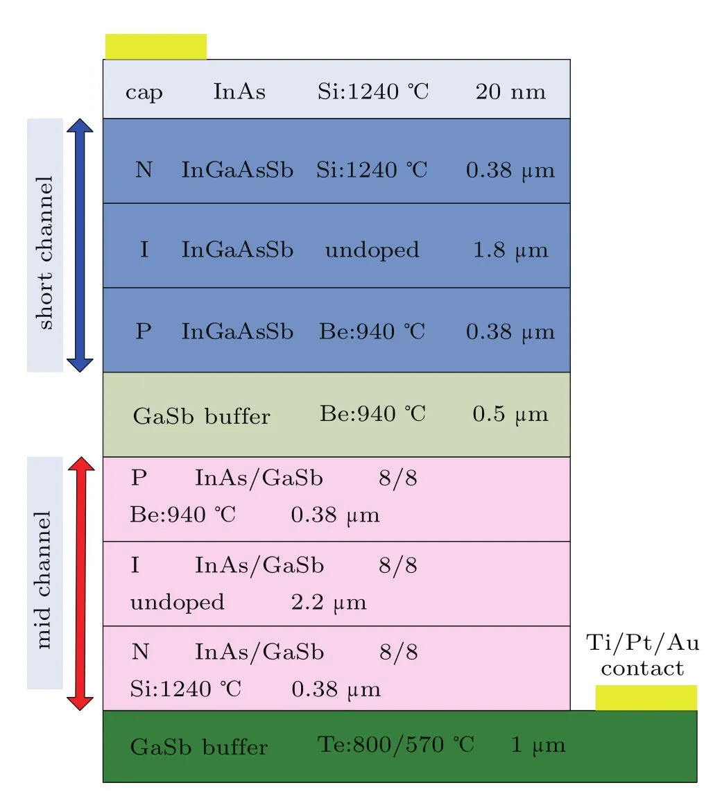
Fig.1.(color online)Schematic of dual-band device.
The high-resolution x-ray diffraction(HRXRD)pattern of the device is shown in Fig.2.It exhibited a period of 51.7˚A for the MWIR SLs,which is in good agreement with the designed thickness of 50˚A.The zero-order diffraction peaks show lattice mismatches of 353 arcsec and 97.2 arcsec for the InGaAsSb and MWIR SLs,respectively.Moreover,the material quality was also characterized using an atomic force microscope(AFM).It showed a root mean square(RMS)surface roughness of 1.439˚A over an area of 10×10µm2.
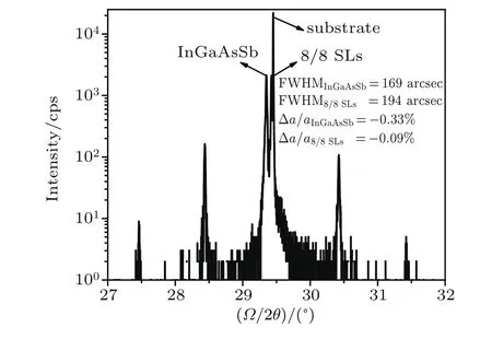
Fig.2.High-resolution x-ray diffraction scan.
2.2.Device fabrication
Fabrication was started with SiO2deposition on wafers as a hard etching mask.SiO2etching was performed for defining the mesas after standard UV photolithography.Then,inductively coupled plasma(ICP)dry etching was performed to the bottom GaSb buffer layer by using gases of CH4/Cl4/Ar2. After the residual SiO2is eliminated using the ICP,the devices were passivated by using anodic sulfide as chemical passivation for filling dangling bonds on the surface.[13]Subsequently,a 200 nm SiO2layer was deposited by ion-beam sputtering deposition(IBSD)as the physical passivation.[14,15]Then,a second photolithography was performed for opening the windows on the SiO2as metal contact holes.The top and bottom metal electrodes were formed using electron beam deposited Ti(500˚A)/Pt(500˚A)/Au(3000˚A).Finally,the fabrication was completed using a standard lift-off process.
3.Results and discussion
The device was wire bonded within a chip fixed in a Dewar,which was cooled to 77 K by using liquid nitrogen. The spectral response shown in Fig.3 was measured by positioning the device as an external photodetector in front of a Bruker Fourier Transform Infrared(FTIR)spectrometer and calibrated using a standard DTGS detector.As shown in Fig.3,the MWIR channel is saturated at−300 mV and the 50%cutoff wavelength is 3.6µm.At+300 mV,the signal transforms to the SWIR completely and saturates at+500 mV. The SWIR channel exhibits 50%cutoff wavelength of 2.2µm.
It is essential to mention that each individual n-i-p detector shows no response bias dependence when operated separately.The spectral response bias dependence of dual-color photodetectors could be explained by the band alignment and built-in voltage in the back-to-back junctions.Figure 4 shows the schematic band alignment of the SWIR–MWIR n-i-p-p-i-n structure.The only band misalignment in this structure is in the junction between SWIR and MWIR p-contacts.As mentioned in Section 2.1,a 0.5µm GaSb p-doped buffer layer was used for separating SWIR from MWIR.Therefore,even the contacts were heavily doped to generate Ohmic contact. Moreover,it is still not easy for the photo-generated holes of the SWIR channel to tunnel through the thick barrier.At zero bias,the SWIR signal is completely blocked by the barrier and the built-in potential of MWIR.Meanwhile,part of the MWIR signal could overcome the built-in potential of SWIR. In the negative bias range,the MWIR channel dominates the photocurrent with the junction reverse biased and saturates at−300 mV.When positive bias is applied,the signal translates from MWIR to SWIR gradually as the SWIR junction is reverse biased and the energy band is moving down.To fully extract the SWIR signal,a saturated positive bias of 500 mV should be applied.
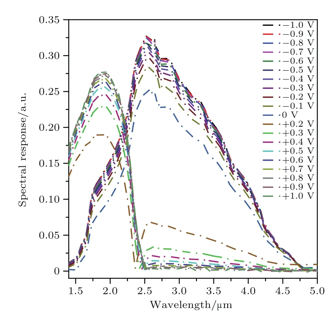
Fig.3.(color online)Spectral response of diode measured at 77 K.
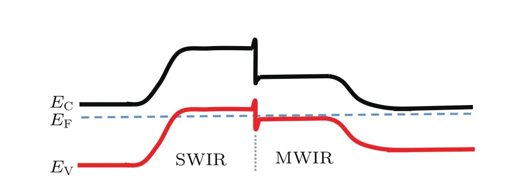
Fig.4.(color online)Schematic band alignment of dual-band detector at zero bias.
The current–voltage characterization was measured and calculated at 200 K.Figure 5 shows the dark current density curve and the differential resistance area(RA)product curve of the devices.For the SWIR channel at+500 mV, the dark current density and RA are 5.93×10⁻⁵A/cm2and 4.5×10³Ω·cm2.At−300 mV,the dark current density and RA are 1.22×10⁻³A/cm2and 1.4×10²Ω·cm2corresponding to the MWIR channel.

Fig.5.(color online)Dark current density and differential resistancearea product vs.applied bias of diode at 200 K.
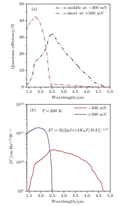
Fig.6.(color online)(a)Quantum efficiency and(b)detectivity.
The optical characterization of the diodes was performed using a FTIR spectrometer and a calibrated blackbody source of 500°C without any anti-reflection(AR)coating. Figure 6(a)shows the QE as a function of wavelength.The MWIR channel exhibited a saturated QE of 31%at 2.6µm, and the SWIR channel exhibited a saturated QE of 42%at 1.8µm.To quantify the optical cross-talk,[16]we use a selectivity parameter S,which is defined as follows:
Then,the dark current short noise limited detectivity (D∗)was calculated for both channels at 200 K.As shown in Fig.6(b),the peak of the MWIR channel D∗is 2.64× 1010cm·Hz1/2/W at 2.6µm,while the SWIR channel exhibits a saturated D∗of 1.54×1011cm·Hz1/2/W at 1.8µm.
4.Conclusions
In this paper,we demonstrate dual-band short-or midwavelength infrared photodetectors using InGaAsSb bulk material and InAs/GaSb super lattice.The 50%cutoff wavelengths are 2.2µm and 3.6µm for the SWIR channel and MWIR channel,respectively.At 200 K,the peak D∗of the MWIR channel and SWIR channel are 2.64× 1010cm·Hz1/2/W and 1.54×1011cm·Hz1/2/W,respectively.
[1]Liu K,Ma W Q,Huang J L,Zhang Y H,Cao Y L,Huang W J and Zhao C C 2016 Acta Phys.Sin.65(in Chinese)
[2]Rehm R,Walther M,Rutz F,Schmitz J,Wörl A,Masur J M,Scheibner R,Wendler J and Ziegler J 2011 J.Electron Mater.40 1738
[3]Rogalski A 2012 Opto-Electronics Review 20 279
[4]Tennant W,Lee D,Zandian M,Piquette E and Carmody M 2008 J Electron.Mater.37 1406
[5]Lee D,Carmody M,Piquette E,Dreiske P,Chen A,Yulius A,Edwall D,Bhargava S,Zandian M and Tennant W 2016 J.Electron.Mater.45 4587
[6]Rogalski A 2008 Opto-Electronics Review 16 458
[7]Höglund L,Ting D,Khoshakhlagh A,Soibel A,Fisher A,Hill C,Keo S,Rafol S and Gunapala S 2016 Appl.Phys.Lett.108 263504
[8]Schuler-Sandy T,Klein B,Casias L,Mathews S,Kadlec C,Tian Z,Plis E,Myers S and Krishna S 2015 J.Crystal Growth 425 29
[9]Haddadi A,Chen G,Chevallier R,Hoang A and Razeghi M 2014 Appl. Phys.Lett.105 121104
[10]Höglund L,Ting D,Soibel A,Fisher A,Khoshakhlagh A,Hill C,Keo S and Gunapala S 2014 Appl.Phys.Lett.105 193510
[11]Hurtado-Castañeda D,Herrera-Perez J L,Arias-Cerón J,Reyes-Betanzo C,Rodriguez-Fragoso P and Mendoza-´Alvarez J 2015 Mater. Sci.Semicond.Process 31 52
[12]Craig A,Jain M,Wicks G,Golding T,Hossain K,McEwan K,Howle C,Percy B and Marshall A 2015 Appl.Phys.Lett.106 201103
[13]Papis-Polakowska E,Kaniewski J,Szade J,Rzodkiewicz W,Jasik A, Jurenczyk J,Orman Z and Wawro A 2014 Thin Solid Films 567 77
[14]Hao H Y,Wang G W,Xiang W,Han X,Xu Y Q,Liao Y P,Zhang Y,Ren Z W,Ni H Q,He Z H and Niu Z C 2015 Infrared Physicsamp; Technology 72 276
[15]Han X,Xiang W,Hao H Y,Jiang D W,Sun Y Y,Wang G W,Xu Y Q and Niu Z C 2017 Chin.Phys.B 26 018505
[16]Jiang D W,Xiang W,Guo F Y,Hong-Yue H,Xi H,Chao L X,Wei W G,Qiang X Y,Jiang X Q and Chuan N Z 2016 Chin.Phys.Lett.33 048502
28 March 2017;revised manuscript
27 April 2017;published online 31 July 2017)
10.1088/1674-1056/26/9/098506
∗Project supported by the National Basic Research Program of China(Grant Nos.2016YFB0402403 and 2013CB932904),the National Natural Science Foundation of China(Grant Nos.61290303 and 61306013),and China Postdoctoral Science Foundation(Grant No.2016M601100).
†Corresponding author.E-mail:zcniu@semi.ac.cn
©2017 Chinese Physical Society and IOP Publishing Ltd http://iopscience.iop.org/cpb http://cpb.iphy.ac.cn
杂志排行

Chinese Physics B的其它文章
- Relationship measurement between ac-Stark shift of 40Ca+clock transition and laser polarization direction∗
- Air breakdown induced by the microwave with two mutually orthogonal and heterophase electric field components∗
- Collective motion of active particles in environmental noise∗
- Temperature dependence of heat conduction coefficient in nanotube/nanowire networks∗
- Analysis of dynamic features in intersecting pedestrian flows∗
- Heat transfer enhancement in MOSFET mounted on different FR4 substrates by thermal transient measurement∗