Heat transfer enhancement in MOSFET mounted on different FR4 substrates by thermal transient measurement∗
2017-08-30NorazlinaDheepanChakravarthiiShanmuganMutharasuandShahromMahmud
Norazlina M S,Dheepan Chakravarthii M K,Shanmugan S,Mutharasu D,and Shahrom Mahmud
School of Physics,Universiti Sains Malaysia 11800 Minden,Penang,Malaysia
Heat transfer enhancement in MOSFET mounted on different FR4 substrates by thermal transient measurement∗
Norazlina M S†,Dheepan Chakravarthii M K,Shanmugan S,Mutharasu D,and Shahrom Mahmud
School of Physics,Universiti Sains Malaysia 11800 Minden,Penang,Malaysia
Miniaturization of electronic package leads to high heat density and heat accumulation in electronics device,resulting in short life time and premature failure of the device.Junction temperature and thermal resistance are the critical parameters that determine the thermal management and reliability in electronics cooling.Metal oxide field effect transistor(MOSFET) is an important semiconductor device for light emitting diode-integrated circuit(LED IC)driver application,and thermal management in MOSFET is a major challenge.In this study,investigations on thermal performance of MOSFET are performed for evaluating the junction temperature and thermal resistance.Suitable modifications in FR4 substrates are proposed by introducing thermal vias and copper layer coating to improve the thermal performance of MOSFET.Experiments are conducted using thermal transient tester(T3ster)at 2.0 A input current and ambient temperature varying from 25°C to 75°C.The thermal parameters are measured for three proposed designs:FR4 with circular thermal vias,FR4 with single strip of copper layer and embedded vias,and FR4 with I-shaped copper layer,and compared with that of plain FR4 substrate.From the experimental results,FR4I−shapedshows promising results by 33.71%reduction in junction temperature and 54.19%reduction in thermal resistance.For elevated temperature,the relative increases in junction temperature and thermal resistance are lower for FR4I−shapedthan those for other substrates considered.The introduction of thermal vias and copper layer plays a significant role in thermal performance.
metal oxide field effect transistor(MOSFET),thermal transient measurement,heat transfer path, FR4
1.Introduction
Thermal management in electronic systems has become a major challenge since its inception in the 20th century.According to the Moore’s law in electronics,the number of transistors in an electronic circuit would be doubled every two years and adversely leading to miniaturization of the electronic components.Thermal management in high power density electronic boards is absolutely necessary for efficient,reliable, durable and perpetual operation.Metal oxide field effect transistor(MOSFET)is a semiconductor device which is widely used in driver circuits and predominantly in light emitting diode-integrated circuit(LED IC)driver circuits due to certain advantages.[1]There are various types of MOSFET packages such as surface mount,through hole and PQFN packages which are classified according to its applications.[2,3]Reduction in size and increase in power density of the MOSFET are analogous resulting in high demand in terms of thermal management.
Good thermal management techniques are required to achieve durable device without exceeding the recommended junction temperature.[4,5]The miniaturization of the device causes the difficulty of thermal management which emerges as a major problem to sustain the device operation in different environments and in rugged system.[6–8]Hence,special attention is paid by researchers around the world,to studying and managing thermal problems in electronic systems as the devices become smaller and smaller over time.
Junction temperature and thermal resistance of semiconductor device are considered as the critical parameters for reliability,device performance and lifetime.In order to measure the junction temperature and thermal resistance of MOSFET, electrical test method is the common and standard measurement method.By using the electrical test method,it is possible to evaluate internal heat flow path of any semiconductor device.Therefore,the heat flow path enables us to detect any internal defect in the device such as void and degradation of thermal interface material.
There are a few methods to evaluate thermal transient such as thermocouple technique,infrared camera and thermal transient measurement.[9–11]Among these three methods, thermal transient measurement is a common tool in thermal characterization of power semiconductor and internal structure analysis.[10]Many researchers and industries focus on thermal transient method in order to characterize thermal performance of any semiconductor device because it is a reliable and non-destructive measurement.Thermal resistance is the quantity measured to evaluate the heat dissipation capacity.Farkas and Simon[12]carried out the studies on the thermal properties of the channel resistance and parasitic elements of insulatedgate devices by using the thermal transient measurement.The change in thermal resistance due to internal serial resistance or in resistance due to individual material was reported.Variation in thermal resistance coefficients due to changes in power dissipation and input current was reported by Lalith et al.[13]Andras et al.[14]conducted the investigations on the simulation based method to eliminate the effect of electrical transients from thermal transient measurements.They suggested that using thermal simulations,the missing initial part of measured thermal transient can be accurately retrieved.Zoltan et al.presented the temperature change induced degradation of SiC MOSFET device.[15]
Printed circuit boards(PCBs)are integral part of any electronic system where the components are mounted on specific substrate in order to obtain the target functions.[16]The choices of MCPCBs and insulated substrates are preferred by PCB manufacturers.[17,18]MCPCBs offer good thermal performances at reasonable cost.In the case of insulated substrates,FR4 and ceramics are widely used substrates as its edges are higher than MCPCBs in terms of weight and cost of the system without compromising the thermal performance.[19]In recent years,many researchers and electronic manufacturers have evolved the thermal vias and copper coated thermal vias for better cooling electronics for small chip packaging.Cho et al.carried out the experiment and simulation on thermal characteristics of glass interposed copper layer through-package vias.[20]From their study the comparison has been made between silicon and glass with vias drilled on both.They found that by the fabrication of thermal vias the thermal performance of interposers has improved.Coppercore MCPCB with thermal vias was investigated by Eveliina at al on high-power COB LED modules.[21]From their investigation,Cu MCPCB showed the outstanding performance on thermal behavior of multichip module by introducing copperfilled microvias.Though many studies were reported in terms of increasing the thermal performance of substrate by suitable coating,confined usage of coating material was not focused due to manufacturing constraints.
In this study,the thermal performances of MOSFETs mounted on FR4 substrate and modified FR4 substrate are discussed,respectively.Three design modifications in FR4 substrates are proposed:FR4 with circular thermal vias,FR4 with single strip of copper layer and embedded vias and FR4 with I-shaped copper layer.The proposed substrates are manufactured by screen-printing process.The thermal performances of MOSFETs mounted on the proposed substrates are determined by thermal transient method by utilizing thermal transient tester(T3ster)system.The Junction temperature and thermal resistance obtained from the experimental measurement are discussed in detail.Heat dissipation capacity and thermal performance for the modified FR4 substrates are compared with those for plain FR4 substrates in order to draw conclusions.
2.Experimental methodology
2.1.Theoretical background
The thermal transient measurement is an electrical test method widely used to characterize the thermal performances of electronic components.The T3ster(Mentor Graphics Corporation)is an instrument to measure the thermal transient which conforms to the JEDEC standards.[22]According to this method,it is not required to remove encapsulation to evaluate the thermal transient.Thermal transient measurement utilizes step function evaluation to gain heating or cooling curve.The heating or cooling curve is defined by temperature measured against response time.
There are four steps in order to obtain thermal transient curve for an electronic component.In the first step,the device under test(DUT)must be calibrated in order to increase the accuracy of the thermal measurement.In the calibration process,a small constant sensor current(1 mA)is needed to calibrate the DUT.Every semiconductor device such as MOSFET, diode,etc,has a temperature-sensitive parameter(TSP).Usually this TSP is responsible for sensing the temperature during the thermal transient testing.For all the device categories, thermal measurement is based on temperature dependence of voltage.[23]The common temperature range for the calibration is from 25°C to 75°C and this graph slope is known as K-factor.The voltage over the DUT is recorded in steps of 10°C until it reaches a steady state with the ambient temperature.Theoretically,K-factor is the correlation of forward voltage(Vf)at constant forward current with junction temperature (TJ),which is given by

where ΔT denotes the change of the temperature-controlled calibration environment with the ambient temperature,ΔVfis the difference in forward voltage.A line is fitted to the measurement points using the least square method.In the second step,powering the device is the most important to heat the device which enables the device to capture heating or cooling curve.The third step and fourth step are to switch on/off and record the temperature transient respectively.
Prior to thermal characterization of any device understanding the operation of thermal transient measurement is mandatory.This equipment is compliant to JEDEC thermal testing standard for electrical test method.According to JEDEC 51 the current jump measurement is suitable for the diode-based device.Current jump can be understood by changing power level to fast switching ON to switching OFF. Figure 1 shows the electrical test method where the total of Idriveand Isense(Imeasurement)was considered as heating current while Imeasurementwas considered as sensing current.
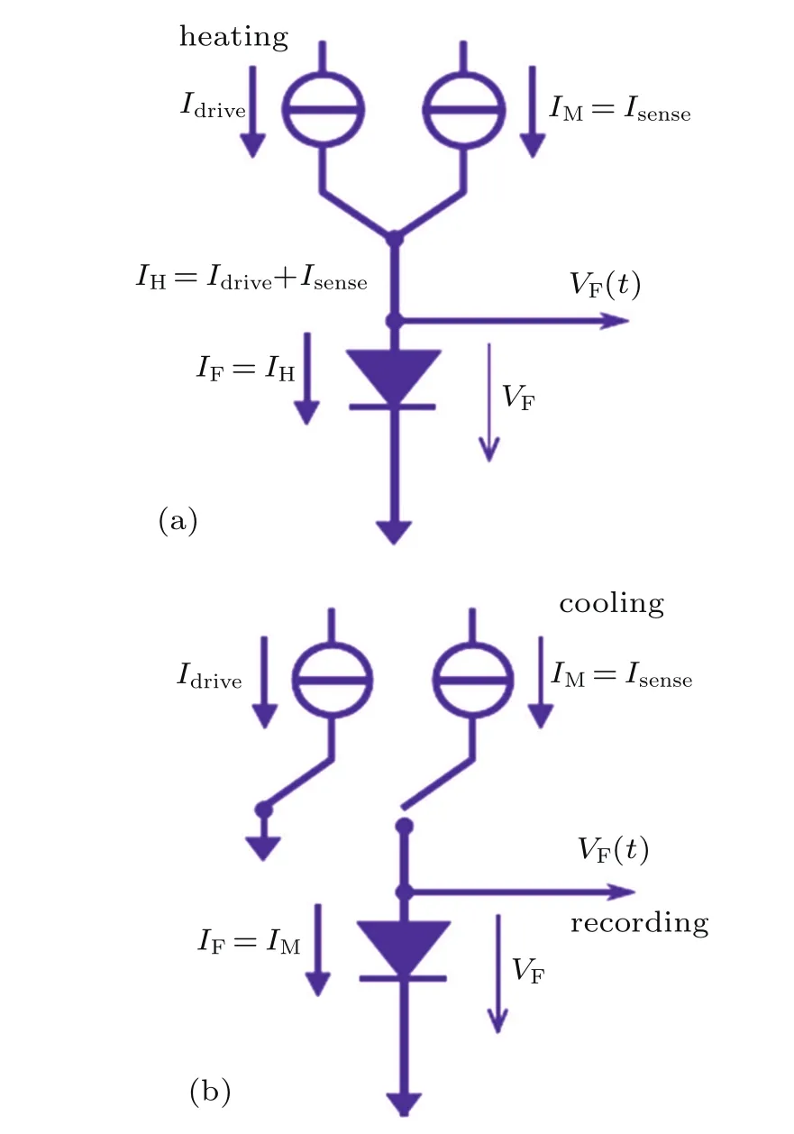
Fig.1.(color online)Practical measurements for(a)heating and(b) cooling configuration of T3Ster.
From the thermal junction measurement response,the cumulative structure function describing the thermal resistance is extracted.[24]The cumulative structure function is a onedimensional description of the thermal path from the heat source to the ambience.Characteristic parts of the thermal resistance curve can be used to identify thermal domains of the measured device.[25]In many cases the thermal domains are difficult to distinguish because the heat flow path is comprised of materials with similar thermal conductivity and good interface quality between the domains.The differential structure function is the derivative of the cumulative structure function which shows even the small changes in thermal resistance as peaks and valleys.
2.2.Thermal resistance and junction temperature
By definition,the thermal resistance from chip junction to the specific environment,Rth,is the temperature difference between the junction and the reference ambient,ΔT,divided by the heating power,Pheat.[26]For integrated circuit(IC)driver components,thermal resistance(Rth)from the junction to solder point is typically given by[27,28]

where TJand TAare the junction temperature and ambient temperature,respectively.The solder point is the thermal contact between the component and the circuit board.The junction temperature(TJ)is defined as the highest temperature of any semiconductor in an electronic device under a maximum operating condition.The difference in temperatures is directly proportional to product of amount of heat transferred from junction to case and the junction-to-case thermal resistance.Maintaining the TJvalue of semiconductor device below its limitis a major challenge in most of the electronic packages.[29,30]Generally,TJvalue depends on three main factors such as power dissipation that determines the amount of heat generated,thermal resistance of substrate and assembly,and ambient condition which dictates how efficiently heat can be removed.
2.3.Description of testing samples
Prior to thermal measurement testing,the description of each substrate is explained in detail.MOSFET of 135 W power is used in this study.The detailed specification of MOSFET is given in Table 1.The range of operating temperature,single pulse avalanched current and voltage are−55 to 150°C,65 A,and 30 V,respectively.The above-mentioned values are at optimal operation of MOSFET and can handle beyond for experimental evaluations.The MOSFET is attached to the substrates through surface mount technology.[31]The schematic layout of the testing samples which is referred to device under test(DUT)as shown in Fig.2.

Table 1.Specification of MOSFET.
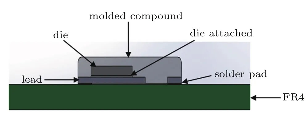
Fig.2.(color online)Schematic layout of DUT-MOSFET mounted on FR4 substrate.
In this study,the MOSFETs are mounted respectively on four substrates and their thermal performances are experimentally evaluated.The specifications and geometric dimensions of different FR4 substrate are given in Table 2.As shown in Fig.3,the substrates are plain FR4(FR4plain),FR4 containing circular thermal vias(FR4vias),FR4 with thermal vias and single strip of Cu layer(FR4ss−vias)and FR4 with I-shaped Cu layer(FR4I−shaped).FR4plainis set as a benchmark substrate and used to analyze the superiority in thermal performance of proposed substrates.The modified FR4 substrates are fabricated by screen-printing process with Cu-layer and identical electrical contacts on top.Circular thermal vias of 0.25 mm in diameter are micro-drilled on FR4 substrates.The thermal vias are directly located beneath the heat source of MOSFET. The prototypes of the proposed FR4 substrates with MOSFET are mounted as shown in Fig.4.

Table 2.Geometrical parameters of different FR4 substrates.
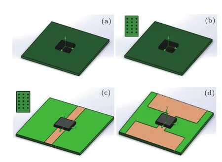
Fig.3.(color online)MOSFETs mounted on(a)FR4plain,(b)FR4vias, (c)FR4ss−vias,and(d)FR4I−shaped,respectively.
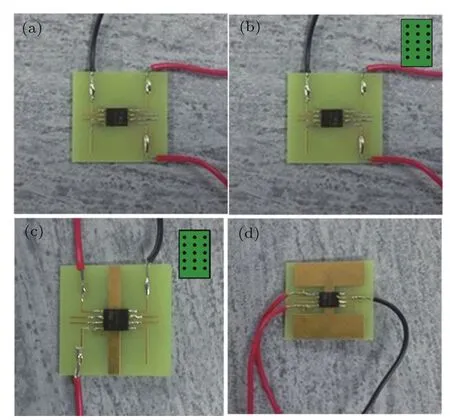
Fig.4.(color online)Developed prototypes of MOSFETs mounted on proposed substrates of(a)FR4plain,(b)FR4vias,(c)FR4ss−vias,and(d) FR4I−shaped,respectively.
The prototypes of the proposed FR4 substrates mounted with MOSFET are attached to the thermostat of T3ster system by using thermal pad.The thickness and thermal conductivity of thermal pad are 0.35 mm and 0.67 W/mK,respectively. In this study,MOSFET is driven at constant current of 2.0 A and voltage of 4.5 V.The MOSFET is subjected to thermal test with above-mentioned operating parameters for duration of 30 s heating time and 120 s cooling time to attain thermal equilibrium for the measurement.During the test,the ambient temperature of the DUT varies from 25°C to 75°C by suitable thermostat regulation.It is important to note that after 30 s of heating time,the MOSFET is switched to sensing current of 1 mA during the cooling time.In this study,the superiority in thermal performance of modified substrates and the influence of ambient temperature on the substrates are reported.
3.Results and discussion
3.1.K-factor
As explained earlier,the MOSFET is calibrated to find the K-factor of DUT.The sensitivity coefficient for the DUT heat source is determined in a calibration measurement by using a temperature controlled thermostat cold plate.The DUT is driven with a small sensor current(1 mA)in order to generate only a negligible amount of heat.The voltages over the DUT are recorded at different temperatures,for example,from 25°C to 75°C in steps of 10°C until it reaches a steady state with the ambient temperature.All calibration curves obtained for investigation on different designs of FR4 substrates are illustrated in Fig.5.From these curves,the k-factor values are obtained and summarized as in Table 3.
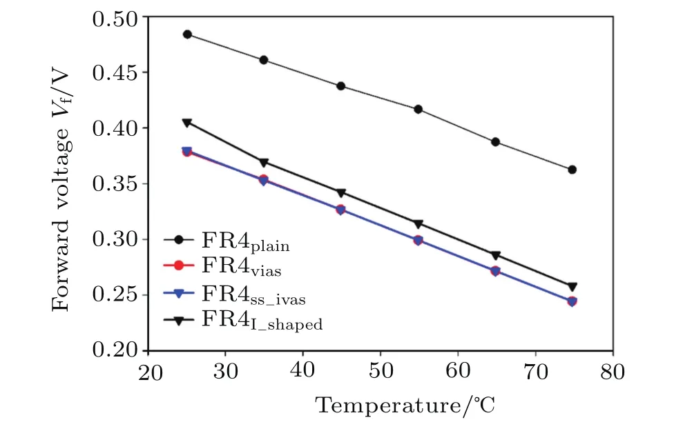
Fig.5.(color online)Calibration curves for different types of FR4 substrates.
The values of K-factor for MOSFET mounted on FR4 with thermal vias,stacked substrate design and heat spreader design are almost the same each with a minimum deviation of 0.33%.This is expected because the MOSFET packages used are of the same type,and should exhibit similar characteristics.

Table 1.Values of K-factors for MOSFET mounted different substrate designs.
3.2.Evaluation of thermal transient measurement
Thermal performances of MOSFETs mounted on FR4plain,FR4vias,FR4ss−vias,and FR4I−shapeddesign for various ambient temperatures are measured using T3Ster.The measured data are processed using T3ster Master Software. Smoothed response curves,differential structure functions and cumulative structure functions obtained for the DUTs are given in Figs.6 and 8 respectively.The prototypes are tested at ambient temperatures varying from 25°C to 75°C in steps of 10°C as explained earlier.
3.2.1.Junction temperature
Figures 6(a)–6(d)illustrate the smoothed response curves measured at different ambient temperatures for the MOSFETs attached on FR4plain,FR4vias,FR4ss−vias,and FR4I−shapedsubstrates respectively.It is obviously seen from the figures that all response curves deviate from each other at different times even though the heating current and voltage are kept constant at 2.0 A and 4.5 V,respectively.Also,the reduction in temperature rise can be seen clearly for proposed FR4 substrates (FR4vias,FR4ss−vias,and FR4I−shaped)in comparison with the scenario for FR4plain.This is due to the enhancement of heat transfer in the substrate by the introduction of thermal vias and Cu layer.Higher thermal conductivity of copper reduces the temperature rise from the MOSFET junction to the ambient temperature which indicates the superiority in thermal performance.It is important to note that the temperature rise decreases with increase in TAin the order of 25°C to 75°C for FR4plainand FR4vias.On the contrary,variable observations are recorded for FR4ss−viasand FR4I−shapeddue to the presence of Cu layer.As TAincreases,the heat conduction by the Cu layer from the ambient contributes to such an invariable performance.[21]For FR4ss−vias,the temperature rise decreases from 25°C to 65°C due to efficient heat dissipation from the junction.At higher TA(75°C),the heat conduction by the Cu layer is dominated over the heat generated at the junction and hence the temperature rise increases.In the case of FR4I−shaped,the temperature rise increases for TAchanging from 25°C to 35°C and decreases thereafter from 35°C to 65°C.This is due to non-linear variation in spreading resistance within Cu layer for increased TAwhere the heat conduction becomes primary and heat spreading is secondary.[33,34]However,a similar elevated temperature rise is observed for higher TAdue to higher heat generation at the junction.Consequently,it changes the total thermal resistance as explained later in this section.
The value of temperature rise(ΔTJ)at the junction of the MOSFET die can be obtained from smoothed response.By using Eq.(3),the junction temperature(TJ)can be calculated. The initial junction temperature,TJ0in Eq.(3)represents the ambient temperature.The calculated values for junction temperature are explained as shown in Fig.7.It is found that the junction temperature increases with increasing ambient temperature at constant current of MOSFET.These results are expected from Eq.(3)as the TJvalues are higher for higher TAsince the lower limit of TJvalue is anchored by TA.
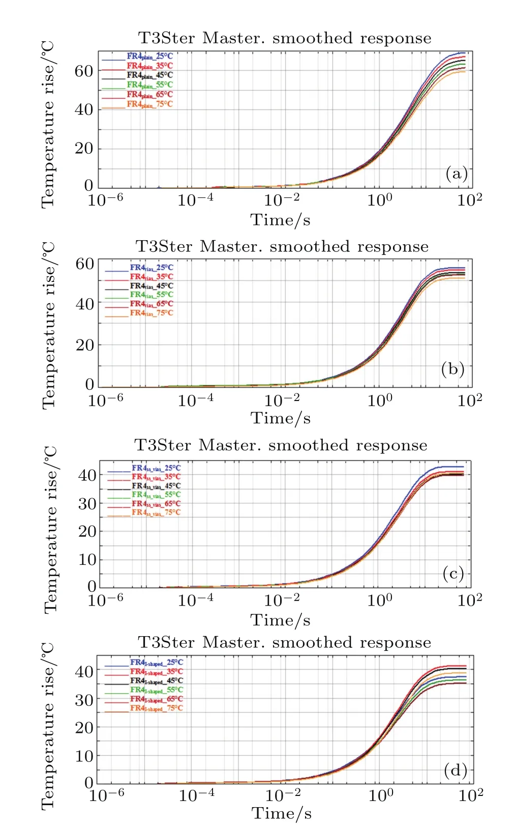
Fig.6.(color online)Plots of temperature rise ΔT versus time for substrates of(a)FR4plain,(b)FR4vias,(c)FR4ss−vias,and(d)FR4I−shaped at various ambient temperatures.
As illustrated in Fig.7,the TJvalue is found to be lower for FR4I−shapedand highest for FR4plaindue to enhanced heat transfer in the proposed substrates.The junction temperature is found to be reduced in the order of FR4I−shaped,FR4ss−vias, FR4vias,and FR4plain.In an attempt to enhance the heat transfer in FRplain,thermal vias are introduced directly beneath the contact to thermal paddle of MOSFET.Evident reduction of 14.08%in TJvalue in comparison with FR4plainoccurs at an ambient temperature of 25°C.TJrises up to 6.36%at an ambient temperature of 75°C.As a matter of fact,it can be correlated to fundamental thermal physics where the heat flows from higher temperature region to lower temperature region to attain thermal equilibrium.The thermal vias acts as an effective medium for heat convection to the ambience which contributes to reduction in TJ.[34]It is quite interesting to look at the thermal performance of FR4ss−viaswhich comprises a single strip Cu layer in addition to thermal vias.The single strip of Cu layer is designed to be parallel to the heat flow path from the junction of MOSFET.[35]The increased in-plane heat conduction in addition to thermal vias that serve as convective medium reduces the value of TJ.The results mentioned above are supported by the fact that at an ambient temperature of 25°C,TJvalue for FR4ss−viasis about 67.96°C while FR4plainand FR4viasare about 94.19°C and 80.93°C,respectively. Additionally,it can be observed that TJvalues of FR4ss−viasand FR4viasare reduced by 26.23°C and 12.98°C compared with that of FR4plain.
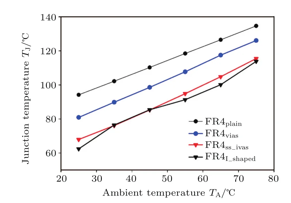
Fig.7.(color online)Variations of T J values of MOSFETs mounted on different substrates with ambient temperature.
Lastly,the extension of Cu layer on FR4 is designed in order to analyze the effect of higher in-plane conduction without the thermal vias.Increased heat spreader surface area of Cu layer is expected to reduce the TJvalue drastically.From Fig.7,the TJvalue of FR4I−shapedis established to be good among the other substrate designs considered.TJis reported to be 33.71%lower than that of FR4plain.However,no significant reduction in TJbetween FR4ss−viasand FR4I−shapedwhich indicates that the presence of thermal vias remains null and void.The major reason for such an observation is that the heat dissipation in thermal vias is dependent on its hole diameter as the effective transport of heat is through the walls rather than via holes.[36,37]Hence,the heat transfer from thermal vias is not so effective as expected at high ambient temperature.On the contrary,the presence of conductive layer in FR4I−shapedincreases heat dissipation.This is due to minimal increase in surface area of Cu layer when a comparison is made between FR4ss−viasand FR4I−shaped.It is important to note that the variation in TJis linear for all the substrates under study except FR4I−shaped.The variation in spreading resistance for axial heat conduction contributes to non-linear increase in TJas explained earlier.[38]
3.2.2.Thermal resistance
To gain an insight into the thermal behaviors of the modifi ed FR4 substrates,evaluations of differential and cumulative structure functions are absolutely necessary to identify the different regions in thermal flow path of DUT.A peak-to-peak region in a differential structure function refers to difference in layer material within the DUT.The internal structure having been analyzed as shown in Fig.1,DUT comprises four peaks which are first peak for die,second peak for die attach(connection between the die and leadframe),third peak for thermal paddle,fourth peak for FR4 substrate,and the rest of the region contributes to partial thermal resistance of thermal pad to the ambience.It should be noted that the first three peaks are common in the entire study due to the representation of similar MOSFET.The importance of analysis is focused beyond the third peak where heat transfer enhancement features are introduced.The differential structure functions for different FR4 substrates at a constant input current of 2.0 A and an ambient temperature of 25°C are shown in Fig.8(a). Based on heat flow path,a number of regions can be divided within the differential structure function.For the FR4plainsubstrate,three regions are identified:first region(Region 1)is from origin to middle of third peak which represents the partial thermal resistance of MOSFET(Rthjs),second region(Region 2)is from middle of third peak to middle of fourth peak towards right,which contributes to the partial thermal resistance of FR4plainsubstrate(Rth−FR4plain),and third region(Region 3)is from middle of fifth peak to end of the curve representing the partial thermal resistance of thermal pad(RthTP)attached to the thermostat of the T3ster system.Rthfrom origin to end of the curve is the total thermal resistance(Rthja)of DUT from the component junction(heat source)to ambient environment.The scope of this study lies in estimating the Rthjsand Rthjato evaluate the performance of MOSFET with respect to the thermal behaviours of modified FR4 substrates. In the above explaination,the region 2 is expected to vary due to the presence of heat transfer enhancement feature.The thermal vias and Cu layer introduced in the proposed substrates induce peaks in the differential structure funtions which affirms the heat transfer behaviour of the DUT.Similar responses are recorded in cumulative structure functions where the representations of peaks can be replaced by plateaus for new layers. Figure 8(b)shows the existence of variation in Rthjabetween different FR4 substrates as proposed.For easier comparison of Rthjabetween different substrate designs,ΔRthja−FR4−vias, Δthja−FR4−SSvias,Δthja−FR4−Ishaped refer to relative differences in thermal resistances of FR4vias,FR4ss−vias,and FR4I−shapedin comparison to FR4plain,respectively.From Figs.8(a)and 8(b),are reduced by 24.47%,48.85%,and 54.19%,respectively. These results can be correlated to the reduction in TJvalue as explained earlier.
Additionally,the partial thermal resistance of MOSFET is found to express a similar reduction in accordance with the performance of the respective DUT.The input current applied to the DUT is not completely utilized by the component where a small portion of input power is used for functional specification while most of the remaining power is eliminated as heat transfers through the junction.Increase in Rthjsrefers to less heat dissipation to ambience.
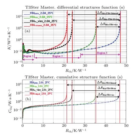
Fig.8.(color online)(a)Differential and(b)cumulative structure functions for different substrates at 25°C ambient temperature.
From the results,it is evident that at a constant input current of 2.0 A,is larger than the R thja−FR4vias,,andFurthermore,the derived structure functions for the proposed substrates shift from left to right in the order of Rthja−FR4plain,Rthja−FR4vias,andThe observation affirms that the thermal conductivity and heat dissipation capacity of the respective substrates contribute to reduction in Rthja.The introduction of thermal vias drastically reduces the Rthja,and significant reduction is observed between the peak 3 and peak 5 which was contributed by the presence of thermal vias in FR4 substrates.In the case of differential structure functions of FR4ss−viasand FR4I−shaped,partial thermal resistance for substrates decreases due to higher thermal conductivity of Cu. Further observation shows that the FR4ss−viaspossesses higher partial thermal resistance due to the presence of thermal vias whereas lower thermal resistanceis reported for FR4I−shaped. Although the surface area of Cu layer in FR4I−shapedis higher than in FR4ss−vias,the presence of thermal vias in FR4ss−viascontributes to higher partial thermal resistance which is evident due to the presence of mild shift in peak and plateau towards right in differential and cumulative structure function as shown in Figs.8(a)and 8(b),respectively.
Figure 9 shows the variations of total thermal resistance obtained from structure functions with ambient temperature for different proposed substrates as explained earlier.It can be observed that Rthjavalues decrease with the increase of ambient temperature for all the proposed substrates.The time taken to reach thermal equilibrium evaluates the efficiency of the heat dissipation system.[34]From the figure,it is evident that the thermal behaviours of all substrates are almost uniform.This indicates that the thermal boundary at the substrates contributes to relative decrease in Rthja.The decrease in Rthjais predominantly by heat conduction from the ambience to FR4 substrates.Further,the influence of ambient temperature on threshold voltage of MOSFET results in reducing Rthjawhich leads to the conclusion that the increased ambient temperature reduces the power step of MOSFET.[39]Altogether, the higher Rthjaresults in higher TJand hence the heat dissipation capacity becomes lower as observed.However,the differences in Rthjawhen the ambient temperature rises from 25°C to 75°C are 5.02%,3.18%,1.96%,and 8.46%for FR4plain, FR4vias,FR4ss−vias,and FR4I−shaped,respectively.This indicates that the FR4I−shapedshows higher thermal performance at elevated ambient temperature with maximum heat dissipation up to 8.46%in comparison with the other substrates.As observed earlier,the Rthof FR4I−shapedshows non-linear reduction unlike the other substrates under study.The variation in thermal performance of FR4I−shapedis attributed to spreading resistance in the Cu layer which is to be accounted in future study.

Fig.9.(color online)Variation of total thermal resistance at different ambient temperatures.
4.Conclusions
In this study,the thermal performances of MOSFETs mounted on different FR4 substrates designed are reported. Thermal behaviour of MOSFET mounted on plain FR4 (FR4plain)substrate is compared with those on modified FR4 substrates such as FR4 with circular thermal vias (FR4vias),FR4 with single strip Copper layer and thermal vias (FR4ss−vias)and FR4 with I-shaped copper heat spreader layer (FR4I−shaped).Thermal performances of different substrates are measured by The T3ster.The junction temperature(TJ) and total thermal resistance(Rthja)are obtained by smoothed response curve and by differential structure functions and cumulative structure functions respectively.For constant input current(2.0 A)and ambient temperature(25°C),FR4I−shapedshows lower TJand Rthjaof 62.44°C and 21.52 K/W respectively.The presence of thermal vias in FR4ss−viaslimits its superiority in thermal performance whereas the utilization of high thermal conductivity material on the substrate proves to reduce the partial thermal resistance within the DUT.Additionally,the influence of ambient temperature on thermal performance of proposed substrate is reported.The Rthjarelatively decreases with the increase of ambient temperature due to predominant heat conduction in the substrate,thereby increasing TJ.This study provides an insight into the enhancement in thermal performance of electronic component by introducing thermal vias and high conductive copper layer in substrates.
Acknowledgment
The authors thank the USAINS Infotech Sdn Bhd for valuable suggestion throughout this project.
[1]Gina Roos,LED Drivers Intergrate MOSFETs,Circuit Protection to Reduce Design Complexity,Digi-Keys Electronics,12.03.2013
[3]Jason Zhang 2004 Choosing the Right Power MOSFET Package,International Rectifier
[4]Weng C J 2009 Int.Com.Heat Mass Transfer 36 245
[5]Robert L 2009 Lifetime of White LEDs.U.S Department of Energy
[6]Krisnamoorthi S,Goh K Y,Chong D Y R,Kaapor R and Sun A Y S 2013 Proceedings of the 5thElectronics Packaging Technology Conference(EPTC 2003),10–12 December,2013,Pan Pacific Hotel,Singapore p.485
[7]Law R C,Cheang R,Tan Y W and Azid I A 2007 International Electronic Manufacturing Technology 31stInternational Conference,8–10 November,2007,Putrajaya,Malaysia p.50
[8]Application Note 2014 Thermal Considerations in Package Design and Selection,Integrated Device Technology,Inc.
[9]Shammas N Y A,Rodriguez M P and Masana F 2002 Microelectron Reliab.42 109
[10]Blackburn D L 2004 Semiconductor Thermal Management and Management Symposium Twentieth Annual IEEE,11 March,2004,San Jose,CA,USA
[11]Katsis D C and Wyk J D V 2003 IEEE Transactions on Industry Applications 39 1239
[12]Farkas G and Simon G 2015 Microelectronics Journal 46 1185
[13]Lalith J,Tianmng D and Nadarajah N 2007 7thInternational Conference on Solid State Lighting,Proceedings of SPIE 6669:666911,26 August,2007,CA,USA
[14]Andras V V,Zoltan S,Attila S and Marta R 2014 Electronic Packaging ICEP 2014 Proceedings 23–25 April,2014,Toyama,Japan p.591
[15]Zoltan S,Weikun Hand Marta R 2006 Thermaland Thermomechanical Phenomena in Electronic Systems(ITherm),2016 15thIEEE Intersociety Conference 31 May–3 June,2016,Las Vegas NV,USA,p.1572
[16]David Kennedy,What are the Functions of a Circuit Board
[17]Winco K C 2007 Journal of the HKPCA 24 12
[18]Horng R H,Hong J S,Tsai Y L,Wuu D S,Chen C M and Chen C J 2010 IEEE Trans.Electron Dev.57 2203
[19]Coonrod J 2011 On Board Technology 26
[20]Cho S,Sundaram V,Tummala R R and Joshi Y K 2015 IEEE Trans. Components,Packaging and Manufacturing Technology 5 1075
[21]Eveliina J,Olli T,Aila S,Markku J,Veli H,Mikko K and Pentti K 2014 IEEE Transactions on Power Electronics 29 1410
[22]Mentor graphics,T3Ster,Mechanical analysis
[23]Lee S Y and Mutharasu D 2011 2nd International Conference on Photonics,17–19 October,2011,Kota Kinabalu,Malaysia,p.1
[24]Székely V and van Bien T 1988 Solid-State Electronics 31 1363
[25]Lasance C J M and Poppe A 2014 Thermal Management for LED Applications(New York:Springer)p.143
[26]Sergent J E and Krum A 1998 Thermal Management Handbook for Electronic Assemblies(New York:McGraw-Hill)
[27]LUXEON Rebel General Purpose White Portfolio,Technical Datasheet DS64.2012.Philips Lumileds Lighting Company
[28]Cree®XLamp®XM-L LEDs,Product Family Data Sheet,CLDDS33 Rev 9A.2010–2013
[29]Package Related Thermal Resistance of LEDs:Osram opto Semiconductor,Application note,page 1–8,January 2014
[30]Thermal Design Considerations:Philips Semiconductor.(2000).
[31]Lin J 2003 US Patent:10 662 289[2003-09-16]
[32]Song S,Lee S and Au V 1994 International Electronics Packaging Conference,May 1994,p.111
[33]Song S,Van A and Kevin P M 1995 Proceedings of the 4th ASME/JSME Thermal Engineering Joint Conference,March 19–24, 1995,Hawaii,United States,p.199
[34]Teeba N,Kean Y L,Chin K L,Anithambigai P,Dinash K and Mutharasu D 2011 3rdAsia Symposium on Quality Electronic Design (ASQED),19–29 July,2011,Kuala Lumpur,Malaysia,p.310
[35]Adrian B 1997 International Journal of Heat and Mass Transfer 49 799
[36]Gautam D,Wager D,Musavi F,Edington M,Eberle W and Dunford W G 2013 28th Annual IEEE Applied Power Electronics Conference and Exposition(APEC),17–21 March,2013,California,USA,p.627
[37]Yang K S,Yang T Y,Tu C W,Yeh C T and Lee M T 2015 Energy Conversion and Management 100 37
[38]Culham J R,Waqar A K,Michael Y and Yuri S M 2007 Journal of Electronic Packaging 129 76
[39]Filanovsky I M and Allam A 2002 IEEE Transactions on Circuits and System I:Fundamental Theory and Apcplications 48 876
15 March 2017;revised manuscript
16 May 2017;published online 31 July 2017)
10.1088/1674-1056/26/9/098901
∗Project supported by the Collaborative Research in Engineering,Scienceamp;Technology(Grant No.P28C2-13).
†Corresponding author.E-mail:ena cr7@yahoo.com
©2017 Chinese Physical Society and IOP Publishing Ltd http://iopscience.iop.org/cpb http://cpb.iphy.ac.cn
杂志排行
Chinese Physics B的其它文章
- Relationship measurement between ac-Stark shift of 40Ca+clock transition and laser polarization direction∗
- Air breakdown induced by the microwave with two mutually orthogonal and heterophase electric field components∗
- Collective motion of active particles in environmental noise∗
- Temperature dependence of heat conduction coefficient in nanotube/nanowire networks∗
- Analysis of dynamic features in intersecting pedestrian flows∗
- Gas-sensor property of single-molecule device:F2 adsorbing effect∗
