Fabrication and characterization of ultra-low noise narrow and wide band Josephson parametric amplifiers∗
2017-08-30KeqiangHuang黄克强QiujiangGuo郭秋江ChaoSong宋超YaruiZheng郑亚锐HuiDeng邓辉YulinWu吴玉林YirongJin金贻荣XiaoboZhu朱晓波andDongningZheng郑东宁
Keqiang Huang(黄克强),Qiujiang Guo(郭秋江),Chao Song(宋超), Yarui Zheng(郑亚锐),Hui Deng(邓辉),Yulin Wu(吴玉林),4, Yirong Jin(金贻荣),Xiaobo Zhu(朱晓波),4,†,and Dongning Zheng(郑东宁),‡
1 Institute of Physics and Beijing National Laboratory for Condensed Matter Physics,Chinese Academy of Sciences,Beijing 100190,China
2 Department of Physics,Zhejiang University,Hangzhou 310027,China
3 School of Physics,University of Chinese Academy of Sciences,Beijing 100190,China
4 CAS Centre for Excellence and Synergetic Innovation Centre in Quantum Information and Quantum Physics, University of Science and Technology of China,Hefei 230026,China
Fabrication and characterization of ultra-low noise narrow and wide band Josephson parametric amplifiers∗
Keqiang Huang(黄克强)1,3,Qiujiang Guo(郭秋江)2,Chao Song(宋超)2, Yarui Zheng(郑亚锐)1,Hui Deng(邓辉)1,Yulin Wu(吴玉林)1,4, Yirong Jin(金贻荣)1,Xiaobo Zhu(朱晓波)1,4,†,and Dongning Zheng(郑东宁)1,3,‡
1 Institute of Physics and Beijing National Laboratory for Condensed Matter Physics,Chinese Academy of Sciences,Beijing 100190,China
2 Department of Physics,Zhejiang University,Hangzhou 310027,China
3 School of Physics,University of Chinese Academy of Sciences,Beijing 100190,China
4 CAS Centre for Excellence and Synergetic Innovation Centre in Quantum Information and Quantum Physics, University of Science and Technology of China,Hefei 230026,China
We have fabricated two types of lumped-element Josephson parameter amplifiers(JPAs)by using a multilayer micro fabrication process involving wet etching of Al films.The first type is a narrow band JPA which shows typical gain above 14 dB in a bandwidth around 35 MHz.The second type is a wideband JPA which is coupled to an input 50 Ω transmission line via an impedance transformer that changes the impedance from about 15 Ω on the non-linear resonator side to 50 Ωon the input transmission line side.The wideband JPA could operate in a 200 MHz range with a gain higher than 14 dB. The amplifiers were used for superconducting qubit readout.The results showed that the signal to noise ratio and hence the readout fidelity were improved significantly.
Josephson parameter amplifier,multilayer micro-fabrication,qubit state readout
1.Introduction
Josephson junction based parametric amplifiers have been studied for decades and are used in a variety of different types of applications,including demonstration of vacuum noise squeezing[1,2]and amplification for extremely sensitive magnetometers.[3]In recent years,the rapid progress of superconducting quantum-bit(qubit)based on Josephson junctions[4–10]has generated renewed interests in Josephson parameter amplifiers(JPA),[9–12]which can provide amplification with near quantum limit noise level and is used as preamplifier for the readout of superconducting qubit quantum states.[13–17]
The most commonly used readout scheme of superconducting qubits at present is the dispersive readout scheme. It relies on detecting microwave photons coming out from a microwave transmission line.In order to distinguish the quantum state of qubits,a good signal to noise ratio is required.In other words,the added noise of preamplifiers should not degrade the signal to noise ratio substantially.However,for the best available commercial high-electron-mobility transistor(HEMT)amplifier operating at low temperatures, the noise temperature is in the range of 2–5 K,that is larger than the photon energy in the dispersive readout transmission line.Taking this into account,it is highly desirable to introduce amplifiers with lower noise temperature.Josephson parametric amplifiers have been regarded as suitable devices for this purpose.So far,a number of different designs have been suggested and demonstrated in experiments.Apart from high gain,JPAs of larger bandwidth are also needed for multiplex readout.
In this paper,we report the fabrication and characterization of two types of Josephson parametric amplifiers which operate with different bandwidths.The first one is of a narrow band with a bandwidth about 35 MHz,while the second one is of a wide band with a bandwidth as large as 200 MHz.The amplifiers are used in superconducting qubit readout experiments,the readout fidelity is improved significantly.
The design of the JPAs we fabricated is similar to the ones reported by Mutus et al.[18]As reported in the literature,the amplifiers are mostly fabricated based on a process using reactive ion etching(RIE)Nb films or inductively coupled plasma (ICP)etching Al films.[18–20]In this work,we fabricate our JPAs using a multilayer micro-fabrication process that is based on wet etch of aluminum films.The wet etching process has the advantage of not requiring the usage of toxic chlorine gas and expensive ICP systems,and is therefore more suitable forsmall scale laboratories.
2.JPA structure and parameters
The schematic circuit diagram of our narrow band parameter amplifier is shown in Fig.1(a).The design of the amplifier is based on the approach reported in Ref.[18].The structure of the amplifier is a 50 Ω transmission line directly coupled to a non-linear LC resonator that is formed by a lumped capacitance shunted with a SQUID that functions as a current dependent non-linear inductor.An on chip bias line,inductively coupled to the SQUID,provides the microwave pump signal and dc bias field.[3]The inductance of the SQUID is inversely proportional to the SQUID critical current IC.Therefore,we may adjust the resonating frequency by varying the critical current via the dc bias field.The resonating frequency is expressed as f=1/2π((LJ+Ls)C)1/2,[21]where C is the capacitance,Lsis the stray inductance in the circuit,and LJis the Josephson inductance that is related to
The amplification of Josephson junction based parametric amplifiers is based on the frequency mixing resulted from the nonlinear Josephson inductance.As the energy source,a sufficiently large pump mode is used to modulate the Josephson inductance of the system,in which the nonlinear Josephson junction plays a key role.During this process,the energy of the pump mode is transferred to the small incident signal mode,which results in the parametric amplification of the incident signal.
The bandwidth of the amplifier is limited by the resonator bandwidth that is inversely proportional to the coupled Q of the resonator to the environment.For a fixed environment impedance Z0(which is typically 50 Ω for the transmission line)and resonant frequency ω0,the coupled Q∼Z0ω0L.In order to reduce Q,one may either increase L or decrease Z0. In this work,we followed the approach in Ref.[18]and fabricated a wide-band JPA by transforming the environmental impedance Z0with a tapered impedance transformer.This approach leads to increased coupling,lowered Q,and simultaneously increased bandwidth and saturation power.The tapered impedance transformer is realized by shunting a CPW of fixed geometry with a series of parallel plate capacitor cross-overs. As pointed out in Ref.[18],the sections with a cross-over approximate a microstrip transmission line,with much lower local characteristic impedance.By varying the density of the cross-overs,the impedance can be varied smoothly.
The Josephson parametric amplifiers discussed here can be operated either in a three-wave mixing mode or a four-wave mixing mode.[18]In this work,we chose the three-wave mixing operation mode.In this mode,the signal is fed into the amplifier through the signal-in port while the pump is applied via the bias line along with the dc bias.The amplified output signal is reflected off the amplifier and sent to the next stage amplifier through the signal-out port.In order to separate the signal-in and signal-out ports,a circulator is used.When the frequency and the amplitude of the pump signal are in appropriate ranges,the nonlinear resonator runs in a parametric amplifier regime.[3,11]
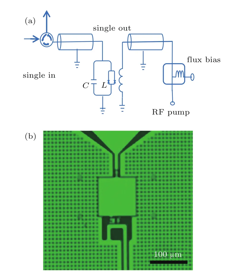
Fig.1.(color online)(a)A schematic diagram of our parameter amplifier.The circle represents the circulator in the measuring circuit.The circulator is used to separate the input signal and output signal.The cylinder represents 50 Ω signal input transmission line and on chip flux bias line.The square represents bias T to combine the RF pump and DC bias.(b)The optical micrograph of our Josephson parameter amplifier.The up triangle pad is the signal input pad,the center square is the parallel plate capacitor,and the down turning line is the on chip bias line.
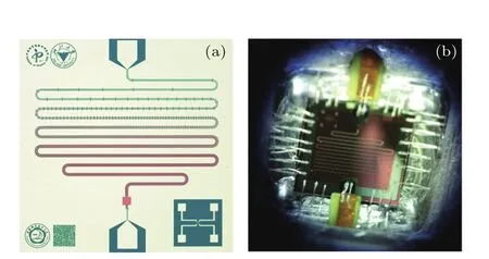
Fig.2.(color online)(a)An optical micrograph of our wide band Josephson parameter amplifier.The up pad is the signal input pad, and the middle line is the signal transition line.With different density crossovers on the transmission line,the transmission line shows different colors from up to down,the crossover changes the impedance of the transmission line.(b)The Josephson parameter amplifier sampler mounted in a sample box.
The optical micrograph in Fig.1(b)shows the amplifier made by a multilayer micro-fabrication process.The parallel plate capacitor has an Al/amorphous Si/Al structure,the capacitance C∼4 pF.The stray inductance of the SQUID loop is around 20 pH and the unbiased Josephson junction nonlinear inductance is around 70 pH.The resonance frequency is around 8 GHz.
In Fig.2,we show a photograph of a wide-band JPA device mounted in a sample box.
3.Sample fabrication process
We adopted a multilayer micro-fabrication process based on wet etching of Al for amplifier fabrication.In Fig.3,the fabrication process is schematically shown.
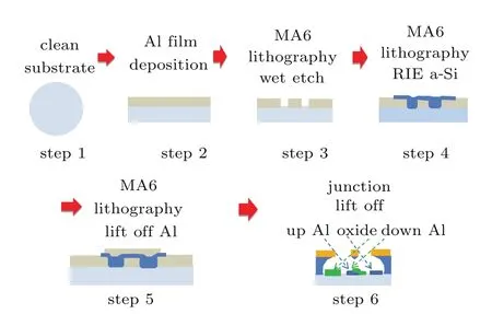
Fig.3.(color online)The schematic diagram of multilayer micro-fabrication process.
The detailed steps are as follows.In the first step,we clean the high resistance silicon substrates(3000 Ω)sequentially in an ultrasonic bath using acetone,alcohol,and deionized water.In each clean,the clean time is about 10 min.In the second step,we deposit 100 nm thick aluminum using an ultra-high vacuum e-beam evaporation system(plasyss 520). In the third step,we use photo lithography(on a Kalsuss MA6 UV aligner)and wet etching to define the capacitor ground electrode,the signal in put and output transmission line,the onchip bias line,the meshed ground plane and position marks. The photo resist used in this step is S1813.For the wet etching process,we use type A solution(http://www.Cemtranse.com). In the fourth step,we grow amorphous silicon as the dielectric layer of the capacitor.The area of the capacitor is again defined by photo lithography and ICP with HBr gas.In the fifth step,we make the top electrode of the capacitor using a lift-off process with LOR5A and S1813 double layer resist mask.
Finally,we made the SQUID using a double-angle evaporation process.[22]The under-cut mask was made using two layers of resist(zip 520 and PMGI).A test SQUID was also made on the chip to check the junction room temperature resistance to see if the SQUID critical current is appropriated.The junction resistance is linked to the junction critical current by the Ambegaokar–Baratoff relation IC=πΔ/2eRn,where Δ is the superconducting energy gap of the electrode and Rnis the junction normal state resistance.
4.Sample characterization and properties analysis
For the characterization of JPAs,a fabricated Josephson parametric amplifier sample was mounted in an aluminum sample box and measured in a cryogen-free dilution refrigerator with a base temperature around 20 mK.The amplifier was operated in the phase preserving mode for the dispersive readout of Xmon qubits which were capacitively coupled to a transmission line through λ/4 coplanar waveguide resonators(CPW).The amplifier was connected to the qubit readout transmission line and the output of the amplifier was further amplified by a HEMT cryogenic amplifier operated at around 3 K,followed by a room temperature microwave amplifier.
Before the measurement,we have measured the phase component of S21versus the dc flux bias and signal frequency, where a periodic structure is observed due to the change of the SQUID critical current with the external magnetic flux.By varying the dc-flux,we can tune the resonant frequency of the nonlinear resonator into the regime for qubit readout.In Fig.4, we show the modulation curve of the phase component for the wide-band JPA sample we made.The solid green line is the guide line to the modulation curve of the SQUID.
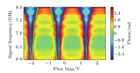
Fig.4.(color online)The phase component of S21 versus dc flux bias and signal frequency of our wide-band JPA sample.
Firstly,we present the results of a narrow-band JPA device.During the measurements,we recorded the S21signal of the qubit readout transmission line.In Fig.5(a),we show the data with the Josephson parametric amplifier on and off,respectively,obtained for fixed pump frequency and amplitude and fixed dc bias.It is obvious that the signal is amplified.In Fig.5(b),the difference of the two S21curves is shown,representing the dependence of the gain on the frequency.The range with the gain higher than 14 dB is about 35 MHz.
In order to further demonstrate the effectiveness of the amplifier for qubit readout,we present the data for different qubit states in Fig.6.In the dispersive readout scheme of the qubit,each qubit is coupled to a readout transmission line via a resonator.By varying the coupling resonator characteristic frequency,it is possible to readout multiple qubits by using one transmission line.

Fig.5.(color online)(a)The response of S21 of the quantum chip with Josephson parameter amplifier pump on and off.(b)Josephson parameter amplifier gain-bandwidth plot,the bandwidth with gain more than 14 dB is about 35 MHz.
The readout of the qubit state is based on the JC model that describes a system containing a two-level atom(qubit) coupled to a resonator.At the large detuning where the qubit and cavity frequency detuning Δ=ωq−ωris much larger than the coupling rate g,the system Hamiltonian is Hdisp=The second part of the Hamiltonian shows that the resonator frequency is shifted by±χ depending on the qubit state operator σz.[7]It is therefore clear that the change of the qubit from the|0〉state to the|1〉state would lead to the change of the resonant frequency.In other words,the resonant peak appeared in the S21curve would shift accordingly.In a practical measurement system,the signal is usually demodulated into in-phase(I)and quadrature(Q)components.In Fig.6,we show the data in the I–Q plane.The red and blue dots represent data points taken for qubits prepared at|0〉and|1〉states,respectively.In this case,we repeated the measurement for 3000 times.In Figs.6(a)and 6(b),we show the data taken with the JPA on and off,respectively.Clearly, when the JPA is on,the separation of the two data point clouds representing the quantum states|0〉and|1〉is larger.The large separation allows faster readout and improved measurement fidelity.[17,23]

Fig.6.(color online)(a),(b)I–Q clouds for the qubit states measured with the JPA pump off and on.The color point represents the single short read out state|0〉(blue)or|1〉(red).The clouds represent the signal scatter by the noise.The bigger black points represent the average centers of the cloud points.The position of the bigger black point represents the position of the state without noise.The dash line connected the center represents the projection axes.The distance of the center represents the relative separation of readout states|0〉and|1〉.(c),(d)The histograms of the readout points with JPA pump off and on,the outlines are Gaussian fits to the histograms and used to estimate the separation fidelity and measurement fidelity.We also estimate the JPA noise temperature by comparing the readout results with JPA off and on.

Fig.7.(color online)(a),(c)The frequency dependence of gain and noise;(b),(d)the signal power dependence of gain and noise.
For the wide-band device,we performed similar measurements.In Figs.7(a)and 7(c),we show the frequency dependence of gain and noise.The results show that the frequency range with amplification above 14 dB is obviously increased as compared to the data shown in Fig.5(a).The estimated JPA noise temperature is around the quantum limit level,[18,24,25]as indicated by the solid red line in Fig.7(c).By monitoring the gain as a function of the input signal power,we found that the saturation power of the JPA is around−115 dB. The wide-band JPA has been used in a number of quantum measurements.[26,27]
5.Conclusion
We have fabricated and characterized a narrow band and a wide band Josephson parametric amplifier.The devices consist of lumped elements and were made using a multilayer micro-fabrication process that is based on wet etch of aluminum films.The wet etching process has the advantage of not requiring the usage of toxic chlorine gas and expensive ICP systems.We believe that the process is therefore more suitable for small scale laboratories.For the narrow band JPA,the frequency band with gain larger than 14 dB is 35 MHz,while the wide band JPA shows over a 200 MHz range.The noise temperature of the JPAs is near the quantum limit.We used the JPA as pre-amplifier to readout superconducting qubit.The results show that the signal to noise ratio is improved significantly,and hence the measurement fidelity is improved.
Acknowledgments
We thank Prof.Haohua Wang for providing the initial designs and for the guidance in measurements.The data were taken at Haohua Wang’s Lab in Zhejiang University.
[1]Yurke B 1987 J.Opt.Soc.Am.B-Opt.Phys.4 1551
[2]Yurke B,Corruccini L R,Kaminsky P G,Rupp L W,Smith A D,Silver A H,Simon R W and Whittaker E A 1989 Phys.Rev.A 39 2519
[3]Hatridge M,Vijay R,Slichter D H,Clarke J and Siddiqi I 2011 Phys. Rev.B 83 134501
[4]Mooij J E,Orlando T P,Levitov L,Tian L,van der Wal C H and Lloyd S 1999 Science 285 1036
[5]Lucero E,Barends R,Chen Y,Kelly J,Mariantoni M,Megrant A, O’Malley P,Sank D,Vainsencher A,Wenner J,White T,Yin Y,Cleland A N and Martinis J M 2012 Nat.Phys.8 719
[6]You J Q,Tsai J S and Nori F 2003 Phys.Rev.B 68 024510
[7]Koch J,Yu T M,Gambetta J,Houck A A,Schuster D I,Majer J,Blais A,Devoret M H,Girvin S M and Schoelkopf R J 2007 Phys.Rev.A 76 19
[8]Reed M D,DiCarlo L,Johnson B R,Sun L,Schuster D I,Frunzio L and Schoelkopf R J 2010 Phys.Rev.A 105 173601
[9]Barends R,Kelly J,Megrant A,Sank D,Jeffrey E,Chen Y,Yin Y, Chiaro B,Mutus J,Neill C,O’Malley P,Roushan P,Wenner J,White T C,Cleland A N and Martinis J M 2013 Phys.Rev.Lett.111 5
[10]Zhong Y P,Li C Y,Wang H H and Chen Y 2013 Chin.Phys.B 22 110313
[11]Levenson-Falk E M,Vijay R and Siddiqi I 2011 Appl.Phys.Lett.98 3
[12]Castellanos-Beltran M A,Irwin K D,Hilton G C,Vale L R and Lehnert K W 2008 Nat.Phys.4 929
[13]Siddiqi I,Vijay R,Pierre F,Wilson C M,Metcalfe M,Rigetti C,Frunzio L and Devoret M H 2004 Phys.Rev.Lett.93 4
[14]Reed M D,DiCarlo L,Johnson B R,Sun L,Schuster D I,Frunzio L and Schoelkopf R J 2010 Phys.Rev.Lett.105 4
[15]Mallet F,Ong F R,Palacios-Laloy A,Nguyen F,Bertet P,Vion D and Esteve D 2009 Nat.Phys.5 791
[16]Lin Z R,Inomata K,Oliver W D,Koshino K,Nakamura Y,Tsai J S and Yamamoto T 2013 Appl.Phys.Lett.103 4
[17]Jeffrey E,Sank D,Mutus J Y,White T C,Kelly J,Barends R,Chen Y, Chen Z,Chiaro B,Dunsworth A,Megrant A,O’Malley P J J,Neill C, Roushan P,Vainsencher A,Wenner J,Cleland A N and Martinis J M 2014 Phys.Rev.Lett.112 5
[18]Mutus J Y,White T C,Jeffrey E,Sank D and Martinis J M 2013 Appl. Phys.Lett.103 122602
[19]Yamamoto T,Inomata K,Watanabe M,Matsuba K,Miyazaki T,Oliver W D,Nakamura Y and Tsai J S 2008 Appl.Phys.Lett.93 3
[20]Bergeal N,Schackert F,Metcalfe M,Vijay R,Manucharyan V E,Frunzio L,Prober D E,Schoelkopf R J,Girvin S M and Devoret M H 2010 Nature 465 64
[21]Barone A and Paterno G 1982 Phaysics and Applications of the Josephson Effect(New York:Wiley)
[22]Wu Y L,Deng H,Yu H F,Xue G M,Tian Y,Li J,Chen Y F,Zhao Shi P and Zheng D N 2013 Chin.Phys.B 22 060309
[23]Sank D T 2014 Fast,Accurate State Measurement in Superconducting Qubits(Ph.D.Dissertation)(Santa Barbara:University of California)
[24]Clerk A A,Devoret M H,Girvin S M,Marquardt F and Schoelkopf R J 2010 Rev.Mod.Phys.82 1155
[25]Caves C M 1982 Phys.Rev.D 26 1817
[26]Song C,Xu K,Liu W X,Yang C,Zheng S B,Deng H,Xie Q,Huang K Q,Guo Q J,Zhang L B,Zhang P F,Xu D,Zheng D N,Zhu X B,Wang H,Chen Y A,Lu C Y,Han S Y and Pan J W 2017 arXiv:170310302 [quant-ph]
[27]Zheng Y,Song C,Chen M C,Xia B X,Liu W X,Guo Q J,Zhang L B, Xu D,Deng H,Huang K Q,Wu Y L,Yan Z G,Zheng D N,Lu L,Pan J W,Wang H,Lu C Y and Zhu X B 2017 Phys.Rev.Lett.118 210504
15 May 2017;published online 18 July 2017)
10.1088/1674-1056/26/9/094203
∗Project supported by the National Natural Science Foundation of China(Grant Nos.91321208,11374344,11404386,11574380,and 11674376),the Ministry of Science and Technology of China(Grant Nos.2014CB921401 and 2016YFA0300601),and the Strategic Priority Research Program of the Chinese Academy of Sciences(Grant No.XDB07010300).
†Corresponding author.E-mail:xbzhu16@ustc.edu.cn
‡Corresponding author.E-mail:dzheng@aphy.iphy.ac.cn
©2017 Chinese Physical Society and IOP Publishing Ltd http://iopscience.iop.org/cpb http://cpb.iphy.ac.cn
猜你喜欢
杂志排行

Chinese Physics B的其它文章
- Relationship measurement between ac-Stark shift of 40Ca+clock transition and laser polarization direction∗
- Air breakdown induced by the microwave with two mutually orthogonal and heterophase electric field components∗
- Collective motion of active particles in environmental noise∗
- Temperature dependence of heat conduction coefficient in nanotube/nanowire networks∗
- Analysis of dynamic features in intersecting pedestrian flows∗
- Heat transfer enhancement in MOSFET mounted on different FR4 substrates by thermal transient measurement∗